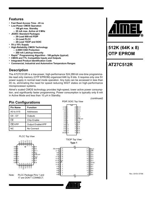
AT27C512 R 512K (64K x 8) OTP EPROM
AT27C512 R 512K (64K x 8) OTP EPROM
AT27C512 R 512K (64K x 8) OTP EPROM

You also want an ePaper? Increase the reach of your titles
YUMPU automatically turns print PDFs into web optimized ePapers that Google loves.
Features<br />
• Fast Read Access Time - 45 ns<br />
• Low-Power CMOS Operation<br />
– 100 µA max. Standby<br />
– 20 mA max. Active at 5 MHz<br />
• JEDEC Standard Packages<br />
– 28-Lead 600-mil PDIP<br />
– 32-Lead PLCC<br />
– 28-Lead TSOP and SOIC<br />
• 5V ± 10% Supply<br />
• High-Reliability CMOS Technology<br />
– 2,000V ESD Protection<br />
– 200 mA Latchup Immunity<br />
• Rapid Programming Algorithm - 100 µs/byte (typical)<br />
• CMOS and TTL Compatible Inputs and Outputs<br />
• Integrated Product Identification Code<br />
• Commercial, Industrial and Automotive Temperature Ranges<br />
Description<br />
The <strong>AT27C512</strong>R is a low-power, high-performance 524,288-bit one-time programmable<br />
read only memory (<strong>OTP</strong> <strong>EPROM</strong>) organized <strong>64K</strong> by 8 bits. It requires only one 5V<br />
power supply in normal read mode operation. Any byte can be accessed in less than<br />
45 ns, eliminating the need for speed reducing WAIT states on high-performance<br />
microprocessor systems.<br />
Atmel’s scaled CMOS technology provides high-speed, lower active power consumption,<br />
and significantly faster programming. Power consumption is typically only 8 mA<br />
in Active Mode and less than 10 µA in Standby.<br />
(continued)<br />
PDIP, SOIC Top View<br />
Pin Configurations<br />
Pin Name<br />
A0 to A15<br />
O0 - O7<br />
CE<br />
OE/VPP<br />
NC<br />
Function<br />
Addresses<br />
Outputs<br />
Chip Enable<br />
Output Enable/VPP<br />
No Connect<br />
PLCC Top View<br />
A7<br />
A12<br />
A15<br />
NC<br />
VCC<br />
A14<br />
A13<br />
A15<br />
A12<br />
A7<br />
A6<br />
A5<br />
A4<br />
A3<br />
A2<br />
A1<br />
A0<br />
O0<br />
O1<br />
O2<br />
GND<br />
1<br />
2<br />
3<br />
4<br />
5<br />
6<br />
7<br />
8<br />
9<br />
10<br />
11<br />
12<br />
13<br />
14<br />
28<br />
27<br />
26<br />
25<br />
24<br />
23<br />
22<br />
21<br />
20<br />
19<br />
18<br />
17<br />
16<br />
15<br />
VCC<br />
A14<br />
A13<br />
A8<br />
A9<br />
A11<br />
OE/VPP<br />
A10<br />
CE<br />
O7<br />
O6<br />
O5<br />
O4<br />
O3<br />
TSOP Top View<br />
Type 1<br />
<strong>512K</strong> (<strong>64K</strong> x 8)<br />
<strong>OTP</strong> <strong>EPROM</strong><br />
<strong>AT27C512</strong>R<br />
<strong>512K</strong> <strong>EPROM</strong><br />
Note:<br />
A6<br />
A5<br />
A4<br />
A3<br />
A2<br />
A1<br />
A0<br />
NC<br />
O0<br />
5<br />
6<br />
7<br />
8<br />
9<br />
10<br />
11<br />
12<br />
13<br />
4<br />
3<br />
2<br />
1<br />
32<br />
31<br />
30<br />
14<br />
15<br />
16<br />
17<br />
18<br />
19<br />
20<br />
O1<br />
O2<br />
GND<br />
NC<br />
O3<br />
O4<br />
O5<br />
29<br />
28<br />
27<br />
26<br />
25<br />
24<br />
23<br />
22<br />
21<br />
A8<br />
A9<br />
A11<br />
NC<br />
OE/VPP<br />
A10<br />
CE<br />
O7<br />
O6<br />
PLCC Package Pins 1 and<br />
17 are DON’T CONNECT.<br />
OE/VPP<br />
A11<br />
A9<br />
A8<br />
A13<br />
A14<br />
VCC<br />
A15<br />
A12<br />
A7<br />
A6<br />
A5<br />
A4<br />
A3<br />
22<br />
23<br />
24<br />
25<br />
26<br />
27<br />
28<br />
1<br />
2<br />
3<br />
4<br />
5<br />
6<br />
7<br />
21<br />
20<br />
19<br />
18<br />
17<br />
16<br />
15<br />
14<br />
13<br />
12<br />
11<br />
10<br />
9<br />
8<br />
A10<br />
CE<br />
O7<br />
O6<br />
O5<br />
O4<br />
O3<br />
GND<br />
O2<br />
O1<br />
O0<br />
A0<br />
A1<br />
A2<br />
Rev. 0015I–07/98<br />
1
The <strong>AT27C512</strong>R is available in a choice of industry standard<br />
JEDEC-approved one-time programmable (<strong>OTP</strong>)<br />
plastic PDIP, PLCC, SOIC, and TSOP packages. All<br />
devices feature two-line control (CE, OE) to give designers<br />
the flexibility to prevent bus contention.<br />
With <strong>64K</strong> byte storage capability, the <strong>AT27C512</strong>R allows<br />
firmware to be stored reliably and to be accessed by the<br />
system without the delays of mass storage media.<br />
Atmel’s 27C512R has additional features to ensure high<br />
quality and efficient production use. The Rapid Programming<br />
Algorithm reduces the time required to program the<br />
part and guarantees reliable programming. Programming<br />
time is typically only 100 µs/byte. The Integrated Product<br />
Identification Code electronically identifies the device and<br />
manufacturer. This feature is used by industry standard<br />
programming equipment to select the proper programming<br />
algorithms and voltages.<br />
System Considerations<br />
Switching between active and standby conditions via the<br />
Chip Enable pin may produce transient voltage excursions.<br />
Unless accommodated by the system design, these transients<br />
may exceed data sheet limits, resulting in device<br />
non-conformance. At a minimum, a 0.1 µF high frequency,<br />
low inherent inductance, ceramic capacitor should be utilized<br />
for each device. This capacitor should be connected<br />
between the V CC and Ground terminals of the device, as<br />
close to the device as possible. Additionally, to stabilize the<br />
supply voltage level on printed circuit boards with large<br />
<strong>EPROM</strong> arrays, a 4.7 µF bulk electrolytic capacitor should<br />
be utilized, again connected between the V CC and Ground<br />
terminals. This capacitor should be positioned as close as<br />
possible to the point where the power supply is connected<br />
to the array.<br />
2<br />
<strong>AT27C512</strong>R
<strong>AT27C512</strong>R<br />
Block Diagram<br />
Absolute Maximum Ratings*<br />
Temperature Under Bias............................... -55°C to + 125°C<br />
Storage Temperature .................................... -65°C to + 150°C<br />
Voltage on Any Pin with<br />
Respect to Ground ........................................-2.0V to + 7.0V (1)<br />
Voltage on A9 with<br />
*NOTICE: Stresses beyond those listed under “Absolute Maximum<br />
Ratings” may cause permanent damage to<br />
the device. This is a stress rating only and functional<br />
operation of the device at these or any other<br />
conditions beyond those indicated in the operational<br />
sections of this specification is not implied.<br />
Exposure to absolute maximum rating conditions<br />
for extended periods may affect device reliability.<br />
Respect to Ground .....................................-2.0V to + 14.0V (1)<br />
V PP Supply Voltage with<br />
Respect to Ground ......................................-2.0V to + 14.0V (1)<br />
Operating Modes<br />
Note: 1. Minimum voltage is -0.6V dc which may undershoot<br />
to -2.0V for pulses of less than 20 ns. Maximum<br />
output pin voltage is V CC + 0.75V dc which may<br />
overshoot to +7.0 volts for pulses of less than 20 ns.<br />
Mode\Pin CE OE/V PP Ai Outputs<br />
Read V IL V IL Ai D OUT<br />
Output Disable V IL V IH X (1) High Z<br />
Standby V IH X (1) X High Z<br />
Rapid Program (2) V IL V PP Ai D IN<br />
PGM Inhibit V IH V PP X (1) High Z<br />
A0 = V IH or V IL<br />
A1 - A15 = V IL<br />
Product Identification (4) V IL V IL<br />
A9 =V H<br />
(3)<br />
Identification Code<br />
Notes: 1. X can be V IL or V IH .<br />
2. Refer to Programming Characteristics.<br />
3. V H = 12.0 ± 0.5V.<br />
4. Two identifier bytes may be selected. All Ai inputs are held low (V IL ), except A9 which is set to V H and A0 which is toggled low<br />
(V IL ) to select the Manufacturer’s Identification byte and high (V IH ) to select the Device Code byte.<br />
3
DC and AC Operating Conditions for Read Operation<br />
Operating<br />
Temp.(Case)<br />
<strong>AT27C512</strong>R<br />
-45 -55 -70 -90 -12 -15<br />
Com. 0°C - 70°C 0°C - 70°C 0°C - 70°C 0°C - 70°C 0°C - 70°C 0°C - 70°C<br />
Ind. -40°C - 85°C -40°C - 85°C -40°C - 85°C -40°C - 85°C -40°C - 85°C -40°C - 85°C<br />
Auto. -40°C - 125°C -40°C - 125°C -40°C - 125°C -40°C - 125°C<br />
V CC Supply 5V ± 10% 5V ± 10% 5V ± 10% 5V ± 10% 5V ± 10% 5V ± 10%<br />
DC and Operating Characteristics for Read Operation<br />
Symbol Parameter Condition Min Max Units<br />
Com., Ind, ±1 µA<br />
I LI Input Load Current V IN = 0V to V CC<br />
Auto. ±5 µA<br />
I LO<br />
I SB<br />
Output Leakage<br />
Current<br />
V CC<br />
(1)<br />
Standby<br />
Current<br />
V OUT = 0V to V CC<br />
Auto. ±10 µA<br />
Com., Ind, ±5 µA<br />
I SB1 (CMOS), CE = V CC ± 0.3V 100 µA<br />
I SB2 (TTL), CE = 2.0 to V CC + 0.5V 1 mA<br />
I CC V CC Active Current f = 5 MHz, I OUT = 0 mA, CE = V IL 20 mA<br />
V IL Input Low Voltage -0.6 0.8 V<br />
V IH Input High Voltage 2.0 V CC + 0.5 V<br />
V OL Output Low Voltage I OL = 2.1 mA 0.4 V<br />
V OH Output High Voltage I OH = -400 µA 2.4 V<br />
Notes: 1. V CC must be applied simultaneously with or before OE/V PP , and removed simultaneously with or after OE/V PP ..<br />
AC Characteristics for Read Operation<br />
Symbol Parameter<br />
Notes:<br />
Condition<br />
2, 3, 4, 5. - see AC Waveforms for Read Operation.<br />
<strong>AT27C512</strong>R<br />
-45 -55 -70 -90 -12 -15<br />
Min Max Min Max Min Max Min Max Min Max Min Max<br />
t ACC<br />
(3)<br />
Address to Output Delay CE= OE/V PP = V IL 45 55 70 90 120 150 ns<br />
t CE<br />
(2)<br />
CE to Output Delay OE/V PP = V IL 45 55 70 90 120 150 ns<br />
t OE<br />
(2)(3)<br />
OE/V PP to Output Delay CE = V IL 20 25 30 35 35 40 ns<br />
t DF<br />
(4)(5)<br />
OE/V PP or CE High to Output Float, whichever<br />
occurred first<br />
t OH<br />
Output Hold from Address, CE or OE/V PP ,<br />
whichever occurred first<br />
Units<br />
20 20 25 25 30 35 ns<br />
7 7 7 0 0 0 ns<br />
4<br />
<strong>AT27C512</strong>R
<strong>AT27C512</strong>R<br />
AC Waveforms for Read Operation (1)<br />
Notes: 1. Timing measurement reference level is 1.5V for -45 and -55 devices. Input AC drive levels are V IL = 0.0V and V IH = 3.0V.<br />
Timing measurement reference levels for all other speed grades are V OL = 0.8V and V OH = 2.0V. Input AC drive levels are<br />
V IL = 0.45V and V IH = 2.4V.<br />
2. OE/V PP may be delayed up to t CE - t OE after the falling edge of CE without impact on t CE .<br />
3. OE/V PP may be delayed up to t ACC - t OE after the address is valid without impact on t ACC .<br />
4. This parameter is only sampled and is not 100% tested.<br />
5. Output float is defined as the point when data is no longer driven.<br />
Input Test Waveforms and<br />
Measurement Levels<br />
Output Test Load<br />
For -45 and -55 devices only:<br />
t R , t F < 5 ns (10% to 90%)<br />
For -70, -90, -12, -15, and -20 devices:<br />
Note:<br />
C L = 100 pF including jig<br />
capacitance, except for<br />
the -45 and -55 devices,<br />
where C L =30 pF.<br />
t R , t F < 20 ns (10% to 90%)<br />
Pin Capacitance<br />
(f = 1 MHz T = 25°C) (1) Typ Max Units Conditions<br />
C IN 4 6 pF V IN = 0V<br />
C OUT 8 12 pF V OUT = 0V<br />
Note: 1. Typical values for nominal supply voltage. This parameter is only sampled and is not 100% tested.<br />
5
Programming Waveforms (1)<br />
Notes: 1. The Input Timing Reference is 0.8V for V IL and 2.0V for V IH .<br />
2. t OE and t DFP are characteristics of the device but must be accommodated by the programmer.<br />
DC Programming Characteristics<br />
T A = 25 ± 5°C, V CC = 6.5 ± 0.25V, OE/V PP = 13.0 ± 0.25V<br />
Limits<br />
Symbol Parameter Test Conditions<br />
Min<br />
Max<br />
Units<br />
I LI Input Load Current V IN = V IL ,V IH ±10 µA<br />
V IL Input Low Level -0.6 0.8 V<br />
V IH Input High Level 2.0 V CC + 1 V<br />
V OL Output Low Voltage I OL = 2.1 mA 0.4 V<br />
V OH Output High Voltage I OH = -400 µA 2.4 V<br />
I CC2 V CC Supply Current (Program and Verify) 25 mA<br />
I PP2 OE/V PP Current CE = V IL 25 mA<br />
V ID A9 Product Identification Voltage 11.5 12.5 V<br />
6<br />
<strong>AT27C512</strong>R
<strong>AT27C512</strong>R<br />
AC Programming Characteristics<br />
T A = 25 ± 5°C, V CC = 6.5 ± 0.25V, OE/V PP = 13.0 ± 0.25V<br />
Limits<br />
Symbol Parameter Test Conditions (1) Min Max<br />
t AS<br />
Address Setup Time<br />
t OEH<br />
t DS<br />
t AH<br />
OE/V PP Hold Time<br />
Data Setup Time<br />
Address Hold Time<br />
Input Rise and Fall Times<br />
(10% to 90%) 20ns<br />
2<br />
2<br />
0<br />
µs<br />
µs<br />
µs<br />
t DH Data Hold Time<br />
Input Pulse Levels<br />
0.45V to 2.4V<br />
2 µs<br />
t DFP<br />
CE High to<br />
Output Float Delay (2) Input Timing Reference Level<br />
0 130 ns<br />
t VCS V CC Setup Time 0.8V to 2.0V 2 µs<br />
t PW CE Program Pulse Width (3) 95 105 µs<br />
t DV Data Valid from CE (2) Output Timing Reference Level<br />
0.8V to 2.0V<br />
1 µs<br />
t VR OE/V PP Recovery Time 2 µs<br />
OE/V<br />
t PP Pulse Rise<br />
PRT<br />
Time During Programming<br />
50 ns<br />
Notes: 1. V CC must be applied simultaneously or before OE/V PP and removed simultaneously or after OE/V PP .<br />
2. This parameter is only sampled and is not 100% tested. Output Float is defined as the point where data is no longer driven—<br />
see timing diagram.<br />
3. Program Pulse width tolerance is 100 µsec ± 5%.<br />
Units<br />
2 µs<br />
t OES OE/V PP Setup Time 2 µs<br />
Atmel’s 27C512R Integrated Product Identification Code<br />
Codes<br />
Pins<br />
A0 O7 O6 O5 O4 O3 O2 O1 O0<br />
Manufacturer 0 0 0 0 1 1 1 1 0 1E<br />
Device Type 1 0 0 0 0 1 1 0 1 0D<br />
Hex<br />
Data<br />
7
Rapid Programming Algorithm<br />
A 100 µs CE pulse width is used to program. The address<br />
is set to the first location. V CC is raised to 6.5V and OE/V PP<br />
is raised to 13.0V. Each address is first programmed with<br />
one 100 µs CE pulse without verification. Then a verification/reprogramming<br />
loop is executed for each address. In<br />
the event a byte fails to pass verification, up to 10 successive<br />
100 µs pulses are applied with a verification after each<br />
pulse. If the byte fails to verify after 10 pulses have been<br />
applied, the part is considered failed. After the byte verifies<br />
properly, the next address is selected until all have been<br />
checked. OE/V PP is then lowered to V IL and V CC to 5.0V. All<br />
bytes are read again and compared with the original data to<br />
determine if the device passes or fails.<br />
8<br />
<strong>AT27C512</strong>R
<strong>AT27C512</strong>R<br />
Ordering Information<br />
t ACC<br />
I CC (mA)<br />
(ns) Active Standby<br />
45 20 0.1 <strong>AT27C512</strong>R-45JC<br />
<strong>AT27C512</strong>R-45PC<br />
<strong>AT27C512</strong>R-45RC<br />
<strong>AT27C512</strong>R-45TC<br />
20 0.1 <strong>AT27C512</strong>R-45JI<br />
<strong>AT27C512</strong>R-45PI<br />
<strong>AT27C512</strong>R-45RI<br />
<strong>AT27C512</strong>R-45TI<br />
55 20 0.1 <strong>AT27C512</strong>R-55JC<br />
<strong>AT27C512</strong>R-55PC<br />
<strong>AT27C512</strong>R-55RC<br />
<strong>AT27C512</strong>R-55TC<br />
20 0.1 <strong>AT27C512</strong>R-55JI<br />
<strong>AT27C512</strong>R-55PI<br />
<strong>AT27C512</strong>R-55RI<br />
<strong>AT27C512</strong>R-55TI<br />
70 20 0.1 <strong>AT27C512</strong>R-70JC<br />
<strong>AT27C512</strong>R-70PC<br />
<strong>AT27C512</strong>R-70RC<br />
<strong>AT27C512</strong>R-70TC<br />
20 0.1 <strong>AT27C512</strong>R-70JI<br />
<strong>AT27C512</strong>R-70PI<br />
<strong>AT27C512</strong>R-70RI<br />
<strong>AT27C512</strong>R-70TI<br />
20 0.1 <strong>AT27C512</strong>R-70JA<br />
<strong>AT27C512</strong>R-70PA<br />
<strong>AT27C512</strong>R-70RA<br />
Ordering Code Package Operation Range<br />
32J<br />
28P6<br />
28R<br />
28T<br />
32J<br />
28P6<br />
28R<br />
28T<br />
32J<br />
28P6<br />
28R<br />
28T<br />
32J<br />
28P6<br />
28R<br />
28T<br />
32J<br />
28P6<br />
28R<br />
28T<br />
32J<br />
28P6<br />
28R<br />
28T<br />
32J<br />
28P6<br />
28R<br />
Commercial<br />
(0°C to 70°C)<br />
Industrial<br />
(-40°C to 85°C)<br />
Commercial<br />
(0°C to 70°C)<br />
Industrial<br />
(-40°C to 85°C)<br />
Commercial<br />
(0°C to 70°C)<br />
Industrial<br />
(-40°C to 85°C)<br />
Automotive<br />
(-40°C to 125°C)<br />
(continued)<br />
Package Type<br />
32J<br />
28P6<br />
28R<br />
28T<br />
32-Lead, Plastic J-Leaded Chip Carrier (PLCC)<br />
28-Lead, 0.600" Wide, Plastic Dual Inline Package (PDIP)<br />
28-Lead, 0.330" Wide, Plastic Gull Wing Small Outline (SOIC)<br />
28-Lead, Thin Small Outline Package (TSOP)<br />
9
Ordering Information (Continued)<br />
t ACC<br />
(ns)<br />
Active<br />
I CC (mA)<br />
Standby<br />
90 20 0.1 <strong>AT27C512</strong>R-90JC<br />
<strong>AT27C512</strong>R-90PC<br />
<strong>AT27C512</strong>R-90RC<br />
<strong>AT27C512</strong>R-90TC<br />
20 0.1 <strong>AT27C512</strong>R-90JI<br />
<strong>AT27C512</strong>R-90PI<br />
<strong>AT27C512</strong>R-90RI<br />
<strong>AT27C512</strong>R-90TI<br />
20 0.1 <strong>AT27C512</strong>R-90JA<br />
<strong>AT27C512</strong>R-90PA<br />
<strong>AT27C512</strong>R-90RA<br />
120 20 0.1 <strong>AT27C512</strong>R-12JC<br />
<strong>AT27C512</strong>R-12PC<br />
<strong>AT27C512</strong>R-12RC<br />
<strong>AT27C512</strong>R-12TC<br />
20 0.1 <strong>AT27C512</strong>R-12JI<br />
<strong>AT27C512</strong>R-12PI<br />
<strong>AT27C512</strong>R-12RI<br />
<strong>AT27C512</strong>R-12TI<br />
20 0.1 <strong>AT27C512</strong>R-12JA<br />
<strong>AT27C512</strong>R-12PA<br />
<strong>AT27C512</strong>R-12RA<br />
150 20 0.1 <strong>AT27C512</strong>R-15JC<br />
<strong>AT27C512</strong>R-15PC<br />
<strong>AT27C512</strong>R-15RC<br />
<strong>AT27C512</strong>R-15TC<br />
20 0.1 <strong>AT27C512</strong>R-15JI<br />
<strong>AT27C512</strong>R-15PI<br />
<strong>AT27C512</strong>R-15RI<br />
<strong>AT27C512</strong>R-15TI<br />
20 0.1 <strong>AT27C512</strong>R-15JA<br />
<strong>AT27C512</strong>R-15PA<br />
<strong>AT27C512</strong>R-15RA<br />
Ordering Code Package Operation Range<br />
32J<br />
28P6<br />
28R<br />
28T<br />
32J<br />
28P6<br />
28R<br />
28T<br />
32J<br />
28P6<br />
28R<br />
32J<br />
28P6<br />
28R<br />
28T<br />
32J<br />
28P6<br />
28R<br />
28T<br />
32J<br />
28P6<br />
28R<br />
32J<br />
28P6<br />
28R<br />
28T<br />
32J<br />
28P6<br />
28R<br />
28T<br />
32J<br />
28P6<br />
28R<br />
Commercial<br />
(0°C to 70°C)<br />
Industrial<br />
(-40°C to 85°C)<br />
Automotive<br />
(-40°C to 125°C)<br />
Commercial<br />
(0°C to 70°C)<br />
Industrial<br />
(-40°C to 85°C)<br />
Automotive<br />
(-40°C to 125°C)<br />
Commercial<br />
(0°C to 70°C)<br />
Industrial<br />
(-40°C to 85°C)<br />
Automotive<br />
(-40°C to 125°C)<br />
Package Type<br />
32J<br />
28P6<br />
28R<br />
28T<br />
32-Lead, Plastic J-Leaded Chip Carrier (PLCC)<br />
28-Lead, 0.600" Wide, Plastic Dual Inline Package (PDIP)<br />
28-Lead, 0.330" Wide, Plastic Gull Wing Small Outline (SOIC)<br />
28-Lead, Thin Small Outline Package (TSOP)<br />
10<br />
<strong>AT27C512</strong>R
<strong>AT27C512</strong>R<br />
Packaging Information<br />
32J, 32-Lead, Plastic J-Leaded Chip Carrier (PLCC)<br />
Dimensions in Inches and (Millimeters)<br />
JEDEC STANDARD MS-016 AE<br />
28P6, 28-Lead, 0.600" Wide, Plastic Dual Inline<br />
Package (PDIP)<br />
Dimensions in Inches and (Millimeters)<br />
JEDEC STANDARD MS-011 AB<br />
.045(1.14) X 45° PIN NO. 1<br />
IDENTIFY<br />
.025(.635) X 30° - 45°<br />
.012(.305)<br />
.008(.203)<br />
1.47(37.3)<br />
1.44(36.6) PIN<br />
1<br />
.032(.813)<br />
.026(.660)<br />
.050(1.27) TYP<br />
.453(11.5)<br />
.447(11.4)<br />
.495(12.6)<br />
.485(12.3)<br />
.553(14.0)<br />
.547(13.9)<br />
.595(15.1)<br />
.585(14.9)<br />
.300(7.62) REF<br />
.430(10.9)<br />
.390(9.90)<br />
AT CONTACT<br />
POINTS<br />
.022(.559) X 45° MAX (3X)<br />
.530(13.5)<br />
.490(12.4)<br />
.021(.533)<br />
.013(.330)<br />
.030(.762)<br />
.015(3.81)<br />
.095(2.41)<br />
.060(1.52)<br />
.140(3.56)<br />
.120(3.05)<br />
SEATING<br />
PLANE<br />
.220(5.59)<br />
MAX<br />
.161(4.09)<br />
.125(3.18)<br />
.110(2.79)<br />
.090(2.29)<br />
.012(.305)<br />
.008(.203)<br />
1.300(33.02) REF<br />
.065(1.65)<br />
.041(1.04)<br />
.630(16.0)<br />
.590(15.0)<br />
.690(17.5)<br />
.610(15.5)<br />
0<br />
15 REF<br />
.566(14.4)<br />
.530(13.5)<br />
.090(2.29)<br />
MAX<br />
.005(.127)<br />
MIN<br />
.065(1.65)<br />
.015(.381)<br />
.022(.559)<br />
.014(.356)<br />
28R, 28-Lead, 0.330" Wide, Plastic Gull Wing Small<br />
Outline (SOIC)<br />
Dimensions in Inches and (Millimeters)<br />
28T, 28-Lead, Plastic Thin Small Outline Package<br />
(TSOP)<br />
Dimensions in Millimeters and (Inches)*<br />
INDEX<br />
MARK<br />
AREA<br />
11.9 (0.469)<br />
11.7 (0.461)<br />
13.7 (0.539)<br />
13.1 (0.516)<br />
0.55 (0.022)<br />
BSC<br />
0.27 (0.011)<br />
0.18 (0.007)<br />
7.15 (0.281)<br />
REF<br />
8.10 (0.319)<br />
7.90 (0.311)<br />
1.25 (0.049)<br />
1.05 (0.041)<br />
0.20 (0.008)<br />
0.10 (0.004)<br />
0<br />
5<br />
REF<br />
0.20 (0.008)<br />
0.15 (0.006)<br />
0.70 (0.028)<br />
0.30 (0.012)<br />
*Controlling dimension: millimeters<br />
11
Atmel Headquarters<br />
Corporate Headquarters<br />
2325 Orchard Parkway<br />
San Jose, CA 95131<br />
TEL (408) 441-0311<br />
FAX (408) 487-2600<br />
Europe<br />
Atmel U.K., Ltd.<br />
Coliseum Business Centre<br />
Riverside Way<br />
Camberley, Surrey GU15 3YL<br />
England<br />
TEL (44) 1276-686677<br />
FAX (44) 1276-686697<br />
Atmel Operations<br />
Atmel Colorado Springs<br />
1150 E. Cheyenne Mtn. Blvd.<br />
Colorado Springs, CO 80906<br />
TEL (719) 576-3300<br />
FAX (719) 540-1759<br />
Atmel Rousset<br />
Zone Industrielle<br />
13106 Rousset Cedex, France<br />
TEL (33) 4 42 53 60 00<br />
FAX (33) 4 42 53 60 01<br />
Asia<br />
Atmel Asia, Ltd.<br />
Room 1219<br />
Chinachem Golden Plaza<br />
77 Mody Road<br />
Tsimshatsui East<br />
Kowloon, Hong Kong<br />
TEL (852) 27219778<br />
FAX (852) 27221369<br />
Japan<br />
Atmel Japan K.K.<br />
Tonetsu Shinkawa Bldg., 9F<br />
1-24-8 Shinkawa<br />
Chuo-ku, Tokyo 104-0033<br />
Japan<br />
TEL (81) 3-3523-3551<br />
FAX (81) 3-3523-7581<br />
Fax-on-Demand<br />
North America:<br />
1-(800) 292-8635<br />
International:<br />
1-(408) 441-0732<br />
e-mail<br />
literature@atmel.com<br />
Web Site<br />
http://www.atmel.com<br />
BBS<br />
1-(408) 436-4309<br />
© Atmel Corporation 1998.<br />
Atmel Corporation makes no warranty for the use of its products, other than those expressly contained in the Company’s standard warranty<br />
which is detailed in Atmel’s Terms and Conditions located on the Company’s website. The Company assumes no responsibility for<br />
any errors which may appear in this document, reserves the right to change devices or specifications detailed herein at any time without<br />
notice, and does not make any commitment to update the information contained herein. No licenses to patents or other intellectual property<br />
of Atmel are granted by the Company in connection with the sale of Atmel products, expressly or by implication. Atmel’s products are<br />
not authorized for use as critical components in life support devices or systems.<br />
Marks bearing ® and/or are registered trademarks and trademarks of Atmel Corporation.<br />
Terms and product names in this document may be trademarks of others.<br />
Printed on recycled paper.<br />
0015I–07/98/xM