PQI StandardII ICF Card 128MB~8GB WideTemp - Unitronix
PQI StandardII ICF Card 128MB~8GB WideTemp - Unitronix
PQI StandardII ICF Card 128MB~8GB WideTemp - Unitronix

Create successful ePaper yourself
Turn your PDF publications into a flip-book with our unique Google optimized e-Paper software.
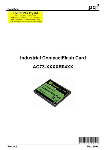
Datasheet<br />
Industrial CompactFlash <strong>Card</strong><br />
AC73-XXXXR04XX<br />
090316009055<br />
Rev. A.5 Mar. 2009
Datasheet<br />
Table of Contents<br />
1. Product Description .....................................................................................................................1<br />
1.1 PRODUCT OVERVIEW.................................................................................................................................................................1<br />
1.2 PRODUCT FEATURE....................................................................................................................................................................1<br />
1.3 SYSTEM REQUIREMENT .............................................................................................................................................................1<br />
2. Specification ................................................................................................................................2<br />
2.1 PHYSICAL SPECIFICATION..........................................................................................................................................................2<br />
2.2 ELECTRONIC SPECIFICATIONS....................................................................................................................................................4<br />
2.3 PERFORMANCE SPECIFICATIONS ................................................................................................................................................5<br />
2.4 ENVIRONMENTAL SPECIFICATION ..............................................................................................................................................5<br />
2.5 RELIABILITY SPECIFICATION......................................................................................................................................................6<br />
2.6 COMPLIANCE SPECIFICATIONS...................................................................................................................................................6<br />
3. Function.......................................................................................................................................7<br />
3.1 PIN SIGNAL ASSIGNMENT ..........................................................................................................................................................7<br />
3.2 CARD PIN SIGNAL DESCRIPTION................................................................................................................................................8<br />
3.3 CARD CAPACITY AND CYLINDER, HEAD, SECTOR....................................................................................................................13<br />
4. Operation Specification..............................................................................................................14<br />
4.1 ABSOLUTE MAXIMUM RATINGS...............................................................................................................................................14<br />
4.2 SERIES TERMINATION REQUIRED FOR ULTRA DMA OPERATION ...............................................................................................14<br />
4.3 ATTRIBUTE MEMORY READ TIMING SPECIFICATION ................................................................................................................15<br />
4.4 CONFIGURATION REGISTER (ATTRIBUTE MEMORY) WRITE TIMING SPECIFICATION ................................................................16<br />
4.5 COMMON MEMORY READ TIMING SPECIFICATION...................................................................................................................17<br />
4.6 COMMON MEMORY WRITE TIMING SPECIFICATION.................................................................................................................18<br />
4.7 I/O INPUT (READ) TIMING SPECIFICATION...............................................................................................................................19<br />
4.8 I/O INPUT (WRITE) TIMING SPECIFICATION .............................................................................................................................20<br />
Rev. A.5 Mar. 2009
Datasheet<br />
4.9 TRUE IDE PIO MODE READ/WRITE TIMING SPECIFICATION ...................................................................................................22<br />
4.10 TRUE IDE MULTIWORD DMA MODE READ/WRITE TIMING SPECIFICATION..........................................................................24<br />
4.11 TRUE IDE ULTRA DMA MODE READ/WRITE TIMING SPECIFICATION ...................................................................................26<br />
4.12 CARD CONFIGURATION..........................................................................................................................................................41<br />
5. CF-ATA Command Set list .........................................................................................................44<br />
6. Ordering Information..................................................................................................................45<br />
Rev. A.5 Mar. 2009
Datasheet<br />
List of Figures<br />
Figure 1: CompactFlash Storage <strong>Card</strong> Overlook Diagram ........................................................... 2<br />
Figure 2: CompactFlash Storage <strong>Card</strong> Dimensions ...................................................................... 3<br />
Figure 3: CompactFlash Storage <strong>Card</strong> Block Diagram................................................................. 4<br />
Figure 4: CompactFlash Storage <strong>Card</strong> Signal Connector................................................................. 7<br />
Figure 5: Ultra DMA termination with Pull-up or Pull down Example ......................................... 15<br />
Figure 6: Attribute Memory Read Timing Diagram....................................................................... 16<br />
Figure 7: Configuration Register (Attribute Memory) Write Timing Diagram.............................. 17<br />
Figure 8: Common Memory Read Timing Diagram ...................................................................... 18<br />
Figure 9: Common Memory Write Timing Diagram...................................................................... 19<br />
Figure 10: I/O Read Timing Diagram............................................................................................. 20<br />
Figure 11: I/O Write Timing Diagram ............................................................................................ 21<br />
Figure 12: True IDE PIO Mode Timing Diagram .......................................................................... 23<br />
Figure 13: True IDE Multiword DMA Read/Write Timing Diagram............................................. 25<br />
Figure 14: Ultra DMA Data-In Burst Initiation Timing ................................................................. 29<br />
Figure 15: Sustained Ultra DMA Data-In Burst............................................................................. 30<br />
Figure 16: Ultra DMA Data-In Burst Host Pause Timing.............................................................. 31<br />
Figure 17: Ultra DMA Data-In Burst Device Termination Timing ................................................ 32<br />
Figure 18: Ultra DMA Data-In Burst Host Termination Timing.................................................... 34<br />
Figure 19: Ultra DMA Data-Out Burst Initiation Timing............................................................... 35<br />
Rev. A.5 Mar. 2009
Datasheet<br />
List of Tables<br />
Table 1: CompactFlash Storage <strong>Card</strong> Physical Dimension........................................................... 3<br />
Table 2 : Compact Flash Storage <strong>Card</strong> Pin Assignment ................................................................... 7<br />
Table 3 : CompactFlash Storage <strong>Card</strong> Pin Signal Description ......................................................... 8<br />
Table 4 : <strong>Card</strong> Capacity and Cylinder, Head, Sector ...................................................................... 13<br />
Table 5: Absolute Maximum Ratings ............................................................................................. 14<br />
Table 6: Typical Series Termination for Ultra DMA...................................................................... 14<br />
Table 7: Attribute Memory Read Timing........................................................................................ 15<br />
Table 8: Configuration Register (Attribute Memory) Write Timing .............................................. 16<br />
Table 9 : Common Memory Read Timing...................................................................................... 17<br />
Table 10 : Common Memory Write Timing ................................................................................... 18<br />
Table 11 : I/O Read Timing ............................................................................................................ 19<br />
Table 12 : I/O Write Timing............................................................................................................ 20<br />
Table 13: True IDE PIO Mode Read/Write Timing........................................................................ 22<br />
Table 14: True IDE Multiword DMA mode Read/Write Timing ................................................... 24<br />
Table 15: Ultra DMA Data Burst Timing Requirements................................................................ 26<br />
Table 16: Ultra DMA Data Burst Timing Descriptions.................................................................. 27<br />
Table 17: Ultra DMA Sender and Recipient IC Timing Requirements.......................................... 28<br />
Table 18: Ultra DMA AC Signal Requirements ............................................................................. 28<br />
Table 19: Attribute Memory Function ............................................................................................ 41<br />
Table 20: PCMCIA Mode I/O Function ......................................................................................... 42<br />
Table 21: Common Memory Function ........................................................................................... 42<br />
Table 22: True IDE mode I/O Function.......................................................................................... 43<br />
Table 23: CF-ATA Command Set List............................................................................................ 44<br />
Table 24: CompactFlash Storage <strong>Card</strong> Ordering Information........................................................ 45<br />
Rev. A.5 Mar. 2009
Datasheet<br />
1. Product Description<br />
1.1 Product Overview<br />
AC73 series is CompactFlash Storage <strong>Card</strong> based on FLASH memory controller technology. This card complies with<br />
CompactFlash specification. It is suitable for the usage of data storage memory for PC or other electric equipment and<br />
Digital Still Camera (DSC). This card is equipped with NAND FLASH memory. By using this card it is possible to<br />
operate stability for the system that has CompactFlash slots.<br />
AC73 series support Fixed and Removable mode, Fixed mode disk use in system storage, some operating system can<br />
not accept boot-up from Removable mode disk like Windows XP, when we boot-up from CompactFlash Storage <strong>Card</strong><br />
with Windows XP, the system detect the device will disable Removable device boot-up function, so the system can not<br />
finish the boot-up process. For this issue, we can setting the device mode to Fixed mode to solve this problem.<br />
The CFC setting to Fixed or Removable mode will no any function different or issue.<br />
• Application Fields;<br />
• Industrial PC and Thin Client<br />
• Entertainment/Consumer Electronic Device<br />
• Game and Telecommunication Machine<br />
• Ticketing, Examining, testing machine<br />
• Army, Health and Production Equipment and Machine<br />
• Other machines and Equipments with CompactFlash <strong>Card</strong> Interface<br />
1.2 Product Feature<br />
• <strong>128MB~8GB</strong> flash memory card<br />
• High performance.<br />
• High reliability.<br />
• Noiseless.<br />
• Robust Error Correction.<br />
• Low power consumption.<br />
• Voltage 3.3V or 5.0V operation.<br />
• PC <strong>Card</strong> ATA protocol compatible.<br />
• True IDE mode compatible.<br />
• Following type I CompactFlash storage card dimensions.<br />
• CompactFlash specification 3.0 version compliant.<br />
• Support PIO Mode 4, Multi-Word DMA 2, and Ultra DMA 2<br />
• Hardware write protect function.<br />
• High Read/Write Speed<br />
• Noiseless operation<br />
: The performance will depend on different platform with different test result.<br />
1.3 System Requirement<br />
- The Host system which is connected to Industrial CompactFlash Storage <strong>Card</strong> should meet system requirements at<br />
minimum;<br />
1.3.1 Power Requirement<br />
• Voltage: DC +3.3V ± 5% or DC +5.0V ± 10%<br />
1.3.2 Operating System<br />
• Windows 98SE/ME/2000/XP/Vista<br />
• Linux, DOS<br />
• WinXP Embedded/WinCE<br />
1.3.3 Interface<br />
• CFA3.0 compatible 50pin SMT connector and type I (3.3mm).<br />
Rev. A.5 1/45 Mar. 2009
Datasheet<br />
2. Specification<br />
2.1 Physical Specification<br />
2.1.1 Overlook<br />
The overlook views of High Speed Industrial CompactFlash Storage <strong>Card</strong> are illustrated in Figure 1.<br />
CompactFlash <strong>Card</strong><br />
Connector<br />
Figure 1: CompactFlash Storage <strong>Card</strong> Overlook Diagram<br />
Writing Protection<br />
Switch<br />
Rev. A.5 2/45 Mar. 2009
Datasheet<br />
2.1.2 Dimension<br />
The Dimensions of CompactFlash Storage <strong>Card</strong> are illustrated in Figure 2 and described in Table 1.<br />
Figure 2: CompactFlash Storage <strong>Card</strong> Dimensions<br />
: The optional notched configuration was shown in the CFA specification Rev. 1.0 in specification Rev. 1.2, the notch was removed for ease<br />
of tooling. This optional configuration can be used but is not recommended.<br />
Table 1: CompactFlash Storage <strong>Card</strong> Physical Dimension<br />
Length<br />
36.4 ±0.15 mm (1.433 ±0.006in.)<br />
Width<br />
Thickness (Including Label Area)<br />
42.8 ±0.10 mm (1.685 ±0.004in.)<br />
3.3 ±0.10mm (0.13 ±0.004in)<br />
2.1.3 Weight<br />
• Weight: 10.5g<br />
Rev. A.5 3/45 Mar. 2009
Datasheet<br />
2.2 Electronic Specifications<br />
2.2.1 Product Definition<br />
The CompacFlash Storage <strong>Card</strong> contains a single chip controller and flash memory module(s) in a matchbook-size<br />
package with a 50-pin connector consisting of two rows of 25 female contacts each on 50 mil (1.27mm) centers. The<br />
controller interfaces with a host system allowing data to be written to and read from the flash memory modules(s).<br />
Figure 3: CompactFlash Storage <strong>Card</strong> Block Diagram<br />
Rev. A.5 4/45 Mar. 2009
Datasheet<br />
2.2.2 Operating Voltage<br />
• Voltage DC +3.3V ± 5% or DC +5.0V ± 10%<br />
2.2.3 Capacity and Block Size information<br />
• Capacity: 128MB ~ 8GB<br />
• Sector Size: 512B<br />
2.2.4 Power Consumption (3.3V/5.0V)<br />
• Current Information<br />
Test Item 3.3V 5.0V<br />
Write Current 45mA 48mA<br />
Read Current 43mA 45mA<br />
Sleep Current 0.4mA 0.6mA<br />
2.3 Performance Specifications<br />
2.3.1 Modes<br />
• Memory <strong>Card</strong> Mode<br />
• I/O <strong>Card</strong> Mode<br />
• True-IDE Mode (PIO Mode: 4, Multi-Word DMA Mode: 2, Ultra DMA Mode: 2)<br />
2.3.2 Data Transfer Time<br />
Dual Mode<br />
• Sequential Read: Up to 20 MB/sec<br />
• Sequential Write: Up to 10 MB/sec<br />
Single Mode<br />
• Sequential Read: Up to 10 MB/sec<br />
• Sequential Write: Up to 5 MB/sec<br />
• Ultra DMA2: 33 MB/sec burst<br />
※ Test Platform:<br />
MB 1: DFI CF4 / Chipset nForce SLI-DR / CPU: AMD146 2.0GHz DDR400: 256MB<br />
MB 2: GIGA 8I945GME / Chipset: Intel 945+ICH7 /CPU: P4-3.0GHz DDR400: 256MB<br />
Testing Software: HD Bench 3.4 / SiSoftware Sandra / Qbench<br />
Testing Operating System: DOS, WinXP<br />
The value is various bases on the testing platform.<br />
2.3.3 Data Retention<br />
• 10years without requiring power support<br />
2.3.4 Wear-leveling<br />
• Dynamic Wear-Leveling for same level of Write/Erase Cycle<br />
2.3.5 Bad Block Management<br />
• The Bad Blocks of Flash Memory will be replaced into new ones by controller.<br />
2.4 Environmental Specification<br />
2.4.1 Temperature<br />
• Operating Temperature: 0ºC to +70ºC, Non Operating Temperature: -40ºC to +85ºC (Industrial type)<br />
• Operating Temperature: -40ºC to +85ºC, Non Operating Temperature: -55ºC to +95ºC (Wide Temperature type)<br />
2.4.2 Humidity<br />
• Operating Humidity (30ºC Max. Wet Bulb Temp): 5% to 95%<br />
• Non-Operating Humidity (30ºC Max. Wet Bulb Temp): 5% to 95% (with no condensation relative humidity)<br />
Rev. A.5 5/45 Mar. 2009
Datasheet<br />
2.4.3 Bare Drop Testing<br />
• Testing Conditions: 100cm height<br />
• Testing Orientation: (Free fell) Front/Rear/Right/Left/Top/Bottom side<br />
• Testing Result: Pass<br />
2.4.4 Vibration<br />
• Random Vibration (Operation) : Testing Specification<br />
Frequency (Hz) PSD (G2/Hz) Acceleration (Grms) Dwell Time (Min)<br />
10 0.01<br />
30min per axis<br />
100 0.08<br />
6Grms<br />
(X‧Y‧Z)<br />
500 0.08<br />
• Random Vibration (Non-Operating): Testing Specification<br />
Frequency (Hz) PSD (G2/Hz) Acceleration (Grms) Dwell Time (Min)<br />
10 0.1<br />
100 0.04<br />
500 0.04<br />
2000 0.004<br />
6Grms<br />
30min per axis<br />
(X‧Y‧Z)<br />
• Frequency Range: 3 ~ 2000Hz<br />
• Testing Result: Pass<br />
2.4.5 Inserted Durability Test<br />
• Testing Condition: 3sec/cycle – Repeated Plug/Unplug 10,000 cycles<br />
• Testing Result: Pass<br />
2.5 Reliability Specification<br />
2.5.1 ECC/EDC (Error Correction Code/Error Detection Code)<br />
• Built-in Reed Solomon 4bytes/sector correction and 5bytes/sector detection.<br />
2.5.2 Read and Program/Erase Cycle<br />
• Read: No Limitation<br />
• Program/Erase: 5,000,000 times<br />
(Estimated on reference to Doc No.SM070001)<br />
2.5.3 MTBF (Mean Time Between Failure)<br />
• 2,000,000 hours<br />
(Estimated on reference to Doc No.SM070002)<br />
2.5.4 Power Cycle<br />
• The Power Cycling is tested to 5000 loop. => “Pass”<br />
2.6 Compliance Specifications<br />
• CE<br />
• FCC<br />
※ Note: Please contact your closest CSS office for other certificate information.<br />
Rev. A.5 6/45 Mar. 2009
Datasheet<br />
3. Function<br />
3.1 Pin Signal Assignment<br />
• The signals assigned for CF <strong>Card</strong> applications are described in Figure 4 and Table 2;<br />
Figure 4: CompactFlash<br />
Connector<br />
Storage <strong>Card</strong> Signal<br />
Table 2 : Compact Flash Storage <strong>Card</strong> Pin Assignment<br />
PC <strong>Card</strong> Memory Mode PC <strong>Card</strong> I/O Mode True IDE Mode<br />
Pin NO. Signal name I/O Signal name I/O Signal name I/O<br />
1 GND - GND - GND -<br />
2 D3 I/O D3 I/O D3 I/O<br />
3 D4 I/O D4 I/O D4 I/O<br />
4 D5 I/O D5 I/O D5 I/O<br />
5 D6 I/O D6 I/O D6 I/O<br />
6 D7 I/O D7 I/O D7 I/O<br />
7 -CE1 I -CE1 I -CS0 I<br />
8 A10 I A10 I A10 I<br />
9 -OE I -OE I -ATA SEL I<br />
10 A9 I A9 I A9 I<br />
11 A8 I A8 I A8 I<br />
12 A7 I A7 I A7 I<br />
13 VCC - VCC - VCC -<br />
14 A6 I A6 I A6 I<br />
15 A5 I A5 I A5 I<br />
16 A4 I A4 I A4 I<br />
17 A3 I A3 I A3 I<br />
18 A2 I A2 I A2 I<br />
19 A1 I A1 I A1 I<br />
20 A0 I A0 I A0 I<br />
21 D0 I/O D0 I/O D0 I/O<br />
22 D1 I/O D1 I/O D1 I/O<br />
23 D2 I/O D2 I/O D2 I/O<br />
24 WP O -IOIS16 O -IOIS16 O<br />
25 -CD2 O -CD2 O -CD2 O<br />
26 -CD1 O -CD1 O -CD1 O<br />
27 D11 I/O D11 I/O D11 I/O<br />
28 D12 I/O D12 I/O D12 I/O<br />
29 D13 I/O D13 I/O D13 I/O<br />
30 D14 I/O D14 I/O D14 I/O<br />
31 D15 I/O D15 I/O D15 I/O<br />
32 -CE2 I -CE2 I -CS1 I<br />
33 -VS1 O -VS1 O -VS1 O<br />
34 -IORD I -IORD I<br />
-IORD<br />
HSTROBE<br />
I<br />
-HDMARDY<br />
35 -IOWR I -IOWR I<br />
-IOWR<br />
STOP<br />
I<br />
36 -WE I -WE I -WE I<br />
37 READY O -IREQ O INTRQ O<br />
38 VCC — VCC — VCC —<br />
39 -CSEL I -CSEL I -CSEL I<br />
40 -VS2 O -VS2 O -VS2 O<br />
41 RESET I RESET I -RESET I<br />
Rev. A.5 7/45 Mar. 2009
Datasheet<br />
PC <strong>Card</strong> Memory Mode PC <strong>Card</strong> I/O Mode True IDE Mode<br />
Pin NO. Signal name I/O Signal name I/O Signal name I/O<br />
42 -WAIT O -WAIT O<br />
IORDY<br />
-DDMARDY<br />
O<br />
DSTROBE<br />
43 -INPACK O -INPACK O DMARQ O<br />
44 -REG I -REG I DMACK I<br />
45 BVD2 I/O -SPKR I/O -DASP I/O<br />
46 BVD1 I/O -STSCHG I/O -PDIAG I/O<br />
47 D8 I/O D8 I/O D8 I/O<br />
48 D9 I/O D9 I/O D9 I/O<br />
49 D10 I/O D10 I/O D10 I/O<br />
50 GND — GND — GND —<br />
3.2 <strong>Card</strong> Pin Signal Description<br />
Table 3 : CompactFlash Storage <strong>Card</strong> Pin Signal Description<br />
Signal Name Dir. Pin No. Description<br />
A10 - A0<br />
(PC <strong>Card</strong> Memory Mode)<br />
A10 - A0<br />
(PC <strong>Card</strong> I/O Mode)<br />
I 8,10,11,12,<br />
14,15,16,17,<br />
18,19,20<br />
These address lines along with the-REG signal are used to selectthe<br />
following: The I/O port address registers within the CompactFlash Storage<br />
<strong>Card</strong> or CF + <strong>Card</strong>, the memory mapped port address registers within the<br />
CompactFlash Storage <strong>Card</strong> or CF+ <strong>Card</strong> , a byte in the card’s information<br />
structure and its configuration control and status registers.<br />
This Signal is the same as the PC <strong>Card</strong> Memory Mode signal.<br />
A2 - A0<br />
(True IDE Mode)<br />
BVD1<br />
(PC <strong>Card</strong> Memory Mode)<br />
-STSCHG<br />
(PC <strong>Card</strong> I/O Mode)<br />
Status Changed<br />
-PDIAG<br />
(True IDE Mode)<br />
BVD2<br />
(PC <strong>Card</strong> Memory Mode)<br />
-SPKR<br />
(PC <strong>Card</strong> / I/O Mode)<br />
-DASP<br />
(True IDE Mode)<br />
-CD1,-CD2<br />
(PC <strong>Card</strong> Memory Mode)<br />
-CD1,-CD2<br />
(PC <strong>Card</strong> Memory Mode)<br />
-CD1,-CD2<br />
(PC <strong>Card</strong> Memory Mode)<br />
18,19,20 In True IDE Mode only A [2:0] are used to select the one of eight registers<br />
in the Task File. The remaining address lines should be grounded by the<br />
host.<br />
I/O 46 This signal is asserted high as BVD1 is not supported.<br />
This signal is asserted low to alert the host to changes in the READY and<br />
Write Protect states; while the I/O interface is configured. Its use is<br />
controlled by the <strong>Card</strong> Config and Status Register.<br />
In the True IDE Mode, this input/output is the Pass Diagnostic signal in the<br />
Master/Slave handshake protocol.<br />
I/O 45 This signal is asserted high, as BVD2 is not supported.<br />
This line is the Binary Audio output from the card. If the <strong>Card</strong> does not<br />
support the Binary Audio function, this line should be held negated.<br />
In the True IDE Mode, this input/output is the Disk Active/Slave Present<br />
signal in the Master/Slave handshake protocol.<br />
O 26,25 These <strong>Card</strong> Detect pins are connected to ground on the CompcatFlash<br />
Storage <strong>Card</strong> or CF+ <strong>Card</strong>. They are used by the host to determine that<br />
the CompactFlash Storage <strong>Card</strong> or CF+ <strong>Card</strong> is fully inserted into its<br />
socket.<br />
This signal is the same for all modes.<br />
This signal is the same for all modes.<br />
Rev. A.5 8/45 Mar. 2009
Datasheet<br />
Signal Name Dir. Pin No. Description<br />
-CE1,-CE2<br />
(PC <strong>Card</strong> I/O Mode)<br />
-CE1,-CE2<br />
(PC <strong>Card</strong> I/O Mode)<br />
<strong>Card</strong> Enable<br />
-CS0,-CS1<br />
(True IDE Mode)<br />
-CSEL<br />
(PC <strong>Card</strong> Memory Mode)<br />
-CSEL<br />
(PC <strong>Card</strong> I/O Mode)<br />
I 7,32 These input signals are used both to select the card and to indicate to the<br />
card whether a byte or a word operation is being performed. –CE2 always<br />
accesses the odd byte of the word. –CE1 accesses the even byte or the<br />
Odd byte of the word depending on A0 and –CE2. A multiplexing scheme<br />
based on A0,-CE1,-CE2 allows 8 bit hosts to access all data on D0 to D7.<br />
This Signal is the same as the PC <strong>Card</strong> Memory Mode signal.<br />
In the True IDE Mode -CS0 is the chip select for the task file registers while<br />
-CS1 is used to select the Alternate Status Register and the Device<br />
Control Register.<br />
While –DMACK is asserted, -CS0 and –CS1 shall be held negated and the<br />
width of the transfers shall be 16 bits.<br />
I 39 This signal is not used for this mode, but should be connected by the host<br />
to PC <strong>Card</strong> A25 or grounded by the host.<br />
This signal is not used for this mode, but should be connected by the host<br />
to PC <strong>Card</strong> A25 or grounded by the host.<br />
-CSEL<br />
(True IDE Mode)<br />
D15 - D00<br />
(PC <strong>Card</strong> Memory Mode)<br />
D15 - D00<br />
(PC <strong>Card</strong> I/O Mode)<br />
I/O 31,30,29,28,<br />
27,49,48,47,<br />
6,5,4,3,2,23,<br />
22,21<br />
This internally pulled up signal is used to configure this device as a Master<br />
or a Slave when configured in the True IDE Mode. When this pin is<br />
grounded, this device is configured as a Master. When the pin is open, this<br />
device is configured as a Slave.<br />
These lines carry the Data, Commands and Status information between<br />
the host and the controller.D00 is the LSB of the Even Byte of the<br />
Word.D08 is the LSB of the Odd Byte of the Word.<br />
This Signal is the same as the PC <strong>Card</strong> Memory Mode signal.<br />
D15 - D00<br />
(True IDE Mode)<br />
GND<br />
(PC <strong>Card</strong> Memory Mode)<br />
GND<br />
(PC <strong>Card</strong> I/O Mode)<br />
GND<br />
(True IDE Mode)<br />
In True IDE Mode, all Task File operations occur in byte mode on the low<br />
order bus D[7:0] while all data transfers are 16 bit using D[15:0].<br />
─ 1,50 Ground.<br />
This signal is the same for all modes.<br />
This signal is the same for all modes.<br />
Rev. A.5 9/45 Mar. 2009
Datasheet<br />
Signal Name Dir. Pin No. Description<br />
-INPCAK<br />
(PC <strong>Card</strong> Memory Mode)<br />
-INPACK<br />
(PC <strong>Card</strong> I/O Mode)<br />
Input Acknowledge<br />
-DMARQ<br />
(True IDE Mode)<br />
O 43 This signal is not used in this mode.<br />
The Input Acknowledge signal is asserted by the CompactFlash Storage<br />
<strong>Card</strong> or CF+ <strong>Card</strong> when the card is selected and responding to an I/O read<br />
cycle at the address that is on the address bus. This signal is used by the<br />
host to control the enable of any input data buffers between the<br />
CompactFlash Storage <strong>Card</strong> or CF+ <strong>Card</strong> and the CPU.<br />
This signal is a DMA Request that is used for DMA data transfers between<br />
host and device. It shall be asserted by the device when it is ready to<br />
transfer data to or from the host. For Multiword DMA transfers, the<br />
direction of data transfer is controlled by –IORD and –IOWR. This signal is<br />
used in a handshake manner with –DMACK, i.e., the device shall wait until<br />
the host asserts –DMACK before negating DMARQ, and reasserting<br />
DMARQ if there is more data to transfer.<br />
DMARQ shall not be driven when the device is not selected.<br />
While a DMA operation is in progress, -CS0 and-CS1 shall be held<br />
negated and the width of the transfers shall be 16 bits.<br />
If there is no hardware support for DMA mode in the host, this output<br />
signal is not used and should not be connected at the host. In this case,<br />
the BIOS must report that DMA mode is not supported by the host so that<br />
device drivers will not attempt DMA mode.<br />
-IORD<br />
(PC <strong>Card</strong> Memory Mode)<br />
-IORD<br />
(PC <strong>Card</strong> I/O Mode)<br />
-IORD<br />
(True IDE Mode)<br />
Ultra DMA Protocol Active)<br />
-HDMARDY<br />
(True IDE Mode – In Ultra<br />
DMA Protocol DMA Read)<br />
HSTROBE<br />
(True IDE Mode – In Ultra<br />
DMA Protocol DMA Write)<br />
A host that dose not support DMA mode and implements both PCMCIA<br />
and True-IDE modes of operation need not alter the PCMCIA mode<br />
connections while in True-IDE modes as long as this does not prevent<br />
proper operation in any mode.<br />
I 34 This signal is not used in this mode.<br />
This is an I/O Read strobe generated by the host. This signal gates I/O<br />
data onto the bus from the CompactFlash Storage <strong>Card</strong> or CF +<strong>Card</strong> when<br />
the card is configured to use the I/O interface.<br />
In True IDE Mode, while Ultra DMA mode DMA read is active, this signal<br />
has same function as in PC <strong>Card</strong> I/O Mode.<br />
In True IDE Mode when Ultra DMA mode DMA Read is active, This signal<br />
is asserted by the host to indicate that the host is read to receive Ultra<br />
DMA data-in bursts. The host may negate –HDMARDY to pause an Ultra<br />
DMA transfer.<br />
In True IDE Mode when Ultra DMA mode DMA Write is active, this signal is<br />
the data out strobe generated by the host. Both the rising and falling edge<br />
of HSTROBE cause data to be latched by the device. The host may stop<br />
generating HSTROBE edges to pause an Ultra DMA data-out burst.<br />
Rev. A.5 10/45 Mar. 2009
Datasheet<br />
Signal Name Dir. Pin No. Description<br />
-IOWR<br />
(PC <strong>Card</strong> Memory Mode)<br />
-IOWR<br />
(PC <strong>Card</strong> I/O Mode)<br />
I 35 This signal is not used in this mode.<br />
The I/O Write strobe pulse is used to clock I/O data on the <strong>Card</strong> Data bus<br />
into the CompcatFlash Storage <strong>Card</strong> or CF+ <strong>Card</strong> controller registers<br />
when the CompactFlash Storage <strong>Card</strong> or CF+ <strong>Card</strong> is configured to use<br />
the I/O interface.<br />
The clocking shall occur on the negative to positive edge of the signal<br />
(Trailing edge)<br />
-IOWR<br />
(True IDE Mode – Except<br />
Ultra DMA Protocol)<br />
STOP<br />
(True IDE Mode – Ultra DMA<br />
Protocol Active)<br />
-OE<br />
(PC <strong>Card</strong> Memory Mode)<br />
-OE<br />
(PC <strong>Card</strong> I/O Mode)<br />
-ATA SEL<br />
(True IDE Mode)<br />
In True IDE Mode, While Ultra DMA mode protocol is not active, this signal<br />
has the same function as in PC <strong>Card</strong> I/O mode.<br />
When Ultra DMA mode protocol is supported, this signal must be negated<br />
before entering Ultra DMA mode protocol.<br />
In true IDE Mode, while Ultra DMA mode protocol is active, the assertion of<br />
this signal causes the termination of the Ultra DMA burst.<br />
I 9 This is an Output Enable strobe generated by the host interface. It is used<br />
to read data from the CompactFlash Storage <strong>Card</strong> or CF+ <strong>Card</strong> in Memory<br />
Mode and to read the CIS and configuration registers.<br />
In PC <strong>Card</strong> I/O Mode. This signal is used to read the CIS and configuration<br />
registers.<br />
To enable True IDE Mode this input should be grounded by the host.<br />
READY<br />
(PC <strong>Card</strong> Memory Mode)<br />
O 37 In Memory Mode, this signal is set high when the CompactFlash Storage<br />
<strong>Card</strong> or CF+ <strong>Card</strong> is ready to accept a new data transfer operation and is<br />
held low when the card is busy.<br />
At power up and at Reset, the READY signal is held low (busy) until the<br />
CompactFlash Storage <strong>Card</strong> or CF+ <strong>Card</strong> has completed its power up or<br />
reset function. No access of any type should be made to the<br />
CompactFlash Storage <strong>Card</strong> or CF+ <strong>Card</strong> during this time.<br />
Note, however, that when a card is powered up and used with RESET<br />
continuously disconnected or asserted, the Reset function of the RESET<br />
pin is disabled, Consequently, the continuous assertion of RESET from the<br />
application of power shall not cause the READY signal to remain<br />
continuously in the busy sate.<br />
-IREQ<br />
(PC <strong>Card</strong> I/O Mode)<br />
INTRQ<br />
(True IDE Mode)<br />
I/O Operation - After the CompactFlash Storage <strong>Card</strong> or CF+ <strong>Card</strong> has<br />
been configured for I/O operation, this signal is used as interrupt Request.<br />
This line is strobe low to generate a pulse mode interrupt or held low for a<br />
level mode interrupt.<br />
In True IDE Mode signal is the active high interrupt Request to the host.<br />
Rev. A.5 11/45 Mar. 2009
Datasheet<br />
Signal Name Dir. Pin No. Description<br />
-REG<br />
(PC <strong>Card</strong> Memory Mode)<br />
Attribute Memory Select<br />
-REG<br />
(PC <strong>Card</strong> I/O Mode)<br />
-DMACK<br />
(True IDE Mode)<br />
I 44 This signal is used during Memory Cycles to distinguish between Common<br />
Memory and Register (Attribute) Memory accesses. High for Common<br />
Memory, Low for Attribute Memory.<br />
The signal shall also be active (low) during I/O Cycles when the I/O<br />
address is on the Bus.<br />
This is a DMA Acknowledge signal that is asserted by the host in response<br />
to DMARQ to Initiate DMA transfers.<br />
While DMA operations are not active, the card shall ignore the –DMACK<br />
signal, including a floating condition.<br />
If DMA operation is not supported by a True IDE Mode only host, this<br />
signal should be driven high or connected to VCC by the host.<br />
RESET<br />
(PC <strong>Card</strong> Memory Mode)<br />
A host that does not support DMA mode and implements both PCMCIA<br />
and True-IDE modes of operation need not alter the PCMCIA Mode<br />
connections while in True-IDE mode as long as this does not prevent<br />
proper operation all modes.<br />
I 41 The CompactFlash Storage <strong>Card</strong> or CF+ <strong>Card</strong> is Reset when the RESET<br />
pin is high with the following important exception:<br />
The host may leave the RESET pin open or keep it continually high from<br />
the application of power without causing a continuous Reset of the card,<br />
Under either of these conditions, the card shall emerge from power-up<br />
having completed an initial Reset.<br />
The CompactFlash Storage <strong>Card</strong> or CF+ <strong>Card</strong> is also Reset when the Soft<br />
Reset bit in the <strong>Card</strong> Configuration Option Register is set.<br />
RESET<br />
(PC <strong>Card</strong> I/O Mode)<br />
-RESET<br />
(True IDE Mode)<br />
VCC<br />
(PC <strong>Card</strong> Memory Mode)<br />
VCC<br />
(PC <strong>Card</strong> I/O Mode)<br />
VCC<br />
(True IDE Mode)<br />
-VS1 -VS2<br />
(PC <strong>Card</strong> Memory Mode)<br />
-VS1 -VS2<br />
(PC <strong>Card</strong> I/O Mode)<br />
-VS1 -VS2<br />
(True IDE Mode)<br />
This signal is the same as the PC <strong>Card</strong> Memory Mode signal.<br />
In the True IDE Mode, This input pin is the active low hardware reset from<br />
the host.<br />
─ 13,38 +5V +3.3V power.<br />
This signal is the same for all modes.<br />
This signal is the same for all modes.<br />
O 33,40 Voltage Sense Signals. -VS1 is grounded on the <strong>Card</strong> and sensed by the<br />
Host that the CompactFlash Storage <strong>Card</strong> or CF+ <strong>Card</strong> CIS can be read at<br />
3.3 volts and -VS2 is reserved by PCMCIA for a secondary voltage and is<br />
not connected on the <strong>Card</strong>.<br />
This signal is the same for all modes.<br />
This signal is the same for all modes.<br />
Rev. A.5 12/45 Mar. 2009
Datasheet<br />
Signal Name Dir. Pin No. Description<br />
-WAIT<br />
(PC <strong>Card</strong> Memory Mode)<br />
-WAIT<br />
(PC <strong>Card</strong> Memory Mode)<br />
IORDY<br />
(True IDE mode – Except<br />
Ultra DMA mode)<br />
-DDMARDY<br />
(True IDE mode – Ultra DMA<br />
Write mode)<br />
-DSTROBE<br />
(True IDE mode – Ultra DMA<br />
Read mode)<br />
-WE<br />
(PC <strong>Card</strong> Memory Mode)<br />
-WE<br />
(PC <strong>Card</strong> I/O Mode)<br />
-WE<br />
(True IDE Mode)<br />
WP<br />
(PC <strong>Card</strong> Memory Mode)<br />
-IOIS16<br />
(PC <strong>Card</strong> I/O Mode)<br />
-IOIS16<br />
(True IDE Mode)<br />
O 42 The -WAIT signal is driven low by the CompactFlash Storage <strong>Card</strong> or CF+<br />
<strong>Card</strong> to signal the host to delay completion of a memory or I/O cycle that is<br />
in progress.<br />
This signal is the same as the PC <strong>Card</strong> Memory Mode signal.<br />
In True IDE Mode, except in Ultra DMA modes, this output signal may be<br />
used as IORDY.<br />
In True IDE Mode, when Ultra DMA mode DMA Write is active, this signal<br />
is asserted by the host to indicate that the device is read to receive Ultra<br />
DMA data-in bursts. The device may negate –DDMARDY to pause an<br />
Ultra DMA transfer.<br />
In True IDE Mode, when Ultra DMA mode DMA Write is active, this signal<br />
is the data out strobe generated by the device. Both the rising and falling<br />
edge of DSTROBE cause data to be latched by the host, The device may<br />
stop generating DSTROBE edges to pause an Ultra DMA data-out burst.<br />
I 36 This is a signal driven by the host and used for strobing memory write data<br />
to the registers of the CompactFlash Storage <strong>Card</strong> or CF+ <strong>Card</strong> when the<br />
card is configured I the memory interface mode. It is also used for writing<br />
the configuration registers.<br />
In PC <strong>Card</strong> I/O Mode, this signal is used for writing the configuration<br />
registers.<br />
In True IDE Mode, this input signal is not used and should be connected to<br />
VCC by the host.<br />
O 24 Memory Mode - The CompactFlash Storage <strong>Card</strong> or CF+ <strong>Card</strong> does not<br />
have a write protect switch. This signal is held low after the completion of<br />
the reset initialization sequence.<br />
I/O Operation - When the CompactFlash Storage <strong>Card</strong> or CF+ <strong>Card</strong> is<br />
configured for I/O Operation Pin 24 is used for the –I/O Selected is 16 Bit<br />
Port (-IOIS16) function. A Low signal indicates that a 16 bit or odd byte<br />
only operation can be performed at the addressed port.<br />
In True IDE Mode this output signal is asserted low when this device is<br />
expecting a word data transfer cycle.<br />
3.3 <strong>Card</strong> Capacity and Cylinder, Head, Sector<br />
The table 4 show various capacities available for AC73 series, if your platform does not support auto-detection function<br />
or AC73 series is not identified, we advice can following below Cylinders, Heads, Sectors number to setting your<br />
platform.<br />
Table 4 : <strong>Card</strong> Capacity and Cylinder, Head, Sector<br />
Unformatted Disk No. of<br />
No. of<br />
No. of<br />
Capacity<br />
Cylinders<br />
Heads<br />
Sectors<br />
Disk Total Sector<br />
128MB 480 16 32 245760<br />
256MB 960 16 32 491520<br />
512MB 975 16 63 982800<br />
1GB 1950 16 63 1965600<br />
2GB 3900 16 63 3931200<br />
4GB 7801 16 63 7863408<br />
8GB 15603 16 63 15727824<br />
Rev. A.5 13/45 Mar. 2009
Datasheet<br />
4. Operation Specification<br />
4.1 Absolute Maximum Ratings<br />
Table 5: Absolute Maximum Ratings<br />
Parameter Symbol Rating Unit<br />
Power supply voltage VCC -0.3 ~ +5.6 V<br />
Input voltage Vin -0.3 ~ +5.6 V<br />
(Referenced to GND)<br />
Electric characteristics<br />
Vcc=3.14V~5.5V<br />
Item<br />
Symbol<br />
Value<br />
Min. Standard Max.<br />
Unit<br />
Measuring<br />
conditions<br />
Input voltage<br />
V IH 2.0 - *1 V<br />
(TTL level) V IL - - 0.7 V<br />
Output voltage<br />
V OH 2.2 - *2 V I OH =-2mA~ -24mA<br />
V OL - - 0.4 V I OL =2mA~ 24mA<br />
4.2 Series termination required for Ultra DMA operation<br />
Series termination resistors are required at both the host and the card for operation in any of the Ultra DMA modes,<br />
Table 6 describes typical values for series termination at the host and the device.<br />
Table 6: Typical Series Termination for Ultra DMA<br />
Signal Host Termination Device Termination<br />
-IORD (-HDMARDY, HSTROBE) 22 ohm 82 ohm<br />
-IOWR ( STOP) 22 ohm 82 ohm<br />
-CS0, -CS1 33 ohm 82 ohm<br />
A00, A01, A02 33 ohm 82 ohm<br />
-DMACK 22 ohm 82 ohm<br />
D15 through D00 33 ohm 33 ohm<br />
DMARQ 82 ohm 22 ohm<br />
INTRQ 82 ohm 22 ohm<br />
IORDY (-DDMARDY, DSTROBE) 82 ohm 22 ohm<br />
-RESET 33 ohm 82 ohm<br />
Note – Only those signals requiring termination are listed in this table. If a signal is not listed, series termination is not required for operation in an<br />
Ultra DMA mode. Shows signals also requiring a pull-up or pull down resistor at the host. The actual termination values should be selected to<br />
compensate for transceiver and trace impedance to match the characteristic cable impedance.<br />
Rev. A.5 14/45 Mar. 2009
Datasheet<br />
Figure 5: Ultra DMA termination with Pull-up or Pull down Example<br />
4.3 Attribute Memory Read Timing Specification<br />
Attribute Memory access time is define as 300 ns. Detailed timing specs are shown in Table 7.<br />
Table 7: Attribute Memory Read Timing<br />
Speed Version<br />
300 ns<br />
Item Symbol IEEE Symbol Min ns. Max ns.<br />
Read Cycle Time tc(R) tAVAV 300<br />
Address Access Time ta(A) tAVQV 300<br />
<strong>Card</strong> Enable Access Time ta(CE) tELQV 300<br />
Output Enable Access Time ta(OE) tGLQV 150<br />
Output Disable Time from CE tdis(CE) tEHQZ 100<br />
Output Disable Time from OE tdis(OE) tGHQZ 100<br />
Address Setup Time tsu(A) tAVGL 30<br />
Output Enable Time from CE ten(CE) tELQNZ 5<br />
Output Enable Time from OE ten(OE) tGLQNZ 5<br />
Data valid from Address Change tv(A) tAXQX 0<br />
Note: All times are in nanoseconds. Dout signifies data provided by the CompactFlash Storage <strong>Card</strong> to the system. The –CE signal or both the –OE<br />
signal and the –WE signal shall be de-asserted between consecutive cycle operations.<br />
Rev. A.5 15/45 Mar. 2009
Datasheet<br />
Figure 6: Attribute Memory Read Timing Diagram<br />
4.4 Configuration Register (Attribute Memory) Write Timing Specification<br />
The <strong>Card</strong> Configuration write access time is defined as 250ns. Detailed timing specifications are shown in Table 8.<br />
Table 8: Configuration Register (Attribute Memory) Write Timing<br />
Speed Version<br />
250 ns<br />
Item Symbol IEEE Symbol Min ns. Max ns.<br />
Write Cycle Time tc(W) tAVAV 250<br />
Write Pulse Width tw(WE) tWLWH 150<br />
Address Setup Time tsu(A) tAVWL 30<br />
Write Recovery Time trec(WE) tWMAX 30<br />
Data Setup Time for WE Tsu(D-WEH) tDVWH 80<br />
Data Hold Time th(D) tWMDX 30<br />
Note: All times are in nanoseconds. Din signifies data provide by the system to the CompactFlash Storage <strong>Card</strong>.<br />
Rev. A.5 16/45 Mar. 2009
Datasheet<br />
Figure 7: Configuration Register (Attribute Memory) Write Timing Diagram<br />
4.5 Common Memory Read Timing Specification<br />
Table 9 : Common Memory Read Timing<br />
Cycle Time Mode: 250 ns 120 ns<br />
Item<br />
Symbol<br />
IEEE Min Max Min ns.<br />
Max ns.<br />
Symbol ns. ns.<br />
Output Enable Access Time ta(OE) tGLQV 125 60<br />
Output Disable Time from tdis(OE) tGHQZ<br />
OE<br />
100 60<br />
Address Setup Time tsu(A) tAVGL 30 15<br />
Address Hold Time th(A) tGHAX 20 15<br />
CE setup Before OE tsu(CE) tELGL 0 0<br />
CE Hold following OE th(CE) tGHEH 20 15<br />
Wait Delay Falling from OE tv(WT-OE) tGLWTV 35 35<br />
Data Setup for Wait Release tv(WT) tQVWTH 0 0<br />
Wait Width Time 2 tw(WT) tWTLWTH 350 350<br />
Note:<br />
1) –WAIT is not supported in ths mode.<br />
2) The maximum load on –WAIT is 1 LSTTL with 50pF (40pF below 120nsec Cycle Time) total load. All times are in nanoseconds. Dout signifies data<br />
provided by the CompactFlash Storage <strong>Card</strong> to the system. The –WAIT signal may be ignored if the –OE cycle to cycle time is greater than the<br />
Wait Width time. The Max Wait Width time can be determined from the <strong>Card</strong> information Structure. The Wait Width time meets the PCMCIA<br />
specification of 12us but is intentionally less in this specification.<br />
Rev. A.5 17/45 Mar. 2009
Datasheet<br />
4.6 Common Memory Write Timing Specification<br />
Figure 8: Common Memory Read Timing Diagram<br />
Table 10 : Common Memory Write Timing<br />
Cycle Time Mode: 250 ns 120 ns<br />
Item<br />
Symbol<br />
IEEE Min Max Min<br />
Max ns.<br />
Symbol ns. ns. ns.<br />
Data Setup before<br />
tsu tDVWH<br />
WE<br />
(D-WEH)<br />
80 50<br />
Data Hold following th(D) tWMDX<br />
WE<br />
30 15<br />
WE Pulse Width tw(WE) tWLWH 150 70<br />
Address Setup Time tsu(A) tAVWL 30 15<br />
CE Setup before WE tsu(CE) tELWL 0 0<br />
Write Recovery Time trec(WE) tWMAX 30 15<br />
Address Hold Time th(A) tGHAX 20 15<br />
CE Hold following WE th(CE) tGHEH 20 15<br />
Wait Delay Falling<br />
tv tWLWTV<br />
from WE<br />
(WT-WE)<br />
35 35<br />
WE High from Wait tv(WT) tWTHWH<br />
Release<br />
0 0<br />
Wait Width Time 2 tw(WT) tWTLWTH 350 350<br />
Note:<br />
1) –WAIT is not supported in ths mode.<br />
2) The maximum load on –WAIT is 1 LSTTL with 50pF (40pF below 120nsec Cycle Time) total load. All times are in nanoseconds. Din signifies data<br />
provided by the system to the CompactFlash Storage <strong>Card</strong>. The –WAIT signal may be ignored if the –WE cycle to cycle time is greater than the<br />
Wait Width time. The Max Wait Width time can be determined from the <strong>Card</strong> information Structure. The Wait Width time meets the PCMCIA<br />
specification of 12us but is intentionally in this specification.<br />
Rev. A.5 18/45 Mar. 2009
Datasheet<br />
Figure 9: Common Memory Write Timing Diagram<br />
4.7 I/O Input (Read) Timing Specification<br />
Table 11 : I/O Read Timing<br />
Cycle Time Mode: 250 ns 120 ns<br />
Item Symbol IEEE Symbol Min ns.<br />
Max<br />
Max<br />
Min ns.<br />
ns.<br />
ns.<br />
Data Delay after IORD td(IORD) tlGLQV 100 50<br />
Data Hold Following IORD th(IORD) tlGHQX 0 5<br />
IORD Width Time tw(IORD) tlGLIGH 165 70<br />
Address Setup before IORD tsuA(IORD) tAVIGL 70 25<br />
Address Hold following IORD thA(IORD) tlGHAX 20 10<br />
CE Setup before IORD tsuCE(IORD) tELIGL 5 5<br />
CE Hold following IORD thCE(IORD) tlGHEH 20 10<br />
REG Setup before IORD tsuREG(IORD) tRGLIGL 5 5<br />
REG Hold following IORD thREG(IORD) tlGHRGH 0 0<br />
INPACK Delay Falling from IORD 3 tdfINLACK(IORD) tlGLIAL 0 45 0 na 1<br />
INPACK Delay Rising from IORD 3 tdrINPACK(IORD) tlGHIAH 45 na 1<br />
IOIS16 Delay Falling from Address 3 tdfIOIS16 tAVISL 35 na 1<br />
IOIS16 Delay Rising from Address 3 tdrIOIS16(ADR) tAVISH 35 na 1<br />
Wait Delay Falling from IORD 3 tdWT(IORD) tlGLWTL 35 35<br />
Data Delay from Wait Rising 3 td(WT) tWTHQV 0 0<br />
Wait Width Time 3 tw(WT) tWTLWTH 350 350<br />
Notes:<br />
1) –IOIS16 and –INPACK are not supported in this mode.<br />
2) –WAIT is not supported in this mode.<br />
3) Maximum load on –WAIT, -INPACK and –IOIS16 is 1 LSTTL with 50 pF (40pF below 120nsec Cycle Time) total load. All times are in nanoseconds.<br />
Minimum time from –WAIT high to –IORD high is 0 nsec, but minimum –IORD width shall be met. Dout signifies data provided by the<br />
CompactFlash Storage <strong>Card</strong> to the system. Wait Width time meets PCMCIA specification of 12us but is intentionally less in this spec.<br />
Rev. A.5 19/45 Mar. 2009
Datasheet<br />
4.8 I/O Input (Write) Timing Specification<br />
Figure 10: I/O Read Timing Diagram<br />
Table 12 : I/O Write Timing<br />
Cycle Time Mode: 250 ns 120 ns<br />
Item Symbol IEEE Symbol Min ns. Max ns. Min ns. Max ns.<br />
Data Setup before IOWR tsu(IOWR) tDVIWH 60 20<br />
Data Hold Following IOWR th(IOWR) tlWHDX 30 10<br />
IOWR Width Time tw(IOWR) tlWLIWH 165 70<br />
Address Setup before IOWR tsuA(IOWR) tAVIWL 70 25<br />
Address Hold following IOWR thA(IOWR) tlWHAX 20 20<br />
CE Setup before IOWR tsuCE (IOWR) tELIWL 5 5<br />
CE Hold following IOWR thCE (IOWR) tlWHEH 20 20<br />
REG Setup before IOWR tsuREG (IOWR) tRGLIWL 5 5<br />
REG Hold following IOWR thREG (IOWR) tlWHRGH 0 0<br />
IOIS16 Delay Falling From tdfIOIS16 (ADR) tAVISL<br />
Address 3 35 na 1<br />
IOIS16 Delay Rising from tdrIOIS16 (ADR) tAVISH<br />
Address 3 35 na 1<br />
Wait Delay Falling from IOWR 3 tdWT (IOWR) tlWLWTL 35 35<br />
IOWR high from Wait high 3 tdrIOWR (WT) tWTJIWH 0 0<br />
Wait Width Time 3 tw(WT) tWTLWTH 350 350<br />
Notes:<br />
1) –IOIS16 and –INPACK are not supported in this mode.<br />
2) –WAIT is not supported in this mode.<br />
3) Maximum load on –WAIT, -INPACK and –IOIS16 is 1 LSTTL with 50 pF (40pF below 120nsec Cycle Time) total load. All times are in nanoseconds.<br />
Minimum time from –WAIT high to –IOWR high is 0 nsec, but minimum -IOWR width shall be met. Din signifies data provided by the system to the<br />
12us but is intentionally less in this specification.<br />
Rev. A.5 20/45 Mar. 2009
Datasheet<br />
Figure 11: I/O Write Timing Diagram<br />
Rev. A.5 21/45 Mar. 2009
Datasheet<br />
4.9 True IDE PIO Mode Read/Write Timing Specification<br />
The timing diagram for True IDE mode of operation in this section is drawn using the conventions in the ATA-4<br />
specification, which are different than the conventions used in the PCMCIA specification and earlier versions of this<br />
specification. Signals are shown with their asserted state as high regardless of whether the signal is actually negative<br />
or positive true. Consequently, the –IORD, the –IOWR and the –IOCS16 signals are shown in the diagram inverted<br />
from their electrical states on the bus.<br />
Table 13: True IDE PIO Mode Read/Write Timing<br />
Item Mode 0 Mode 1 Mode 2 Mode 3 Mode 4 Note<br />
t0 Cycle Time (min) 600 383 240 180 120 1<br />
t1 Address Valid<br />
to –IORD/-IOWR setup (min)<br />
70 50 30 30 25<br />
t2 -IORD/-IOWR(min) 165 125 100 80 70 1<br />
t2 -IORD/-IOWR(min) Register<br />
(8bit)<br />
290 290 290 80 70 1<br />
t2i -IORD/-IOWR recovery<br />
time(min)<br />
- - - 70 25 1<br />
t3 -IOWR data setup (min) 60 45 30 30 20<br />
t4 -IOWR data hold (min) 30 20 15 10 10<br />
t5 -IORD data setup(min) 50 35 20 20 20<br />
t6 -IORD data hold (min) 5 5 5 5 5<br />
t6Z -IORD data tristate (max) 30 30 30 30 30 2<br />
t7 Address valid to –IOCS16<br />
assertion (max)<br />
90 50 40 n/a n/a 4<br />
t8 Address valid to –IOCS16<br />
released (max)<br />
60 45 30 n/a n/a 4<br />
t9 -IORD/-IOWR to address<br />
valid hold<br />
20 15 10 10 10<br />
tRD Read Data Valid to IORDY<br />
active (min), if IORDY<br />
0 0 0 0 0<br />
initially low after tA<br />
tA IORDY Setup time 35 35 35 35 35 3<br />
tB IORDY Pulse Width (max) 1250 1250 1250 1250 1250<br />
tC IORDY assertion to<br />
release(max)<br />
5 5 5 5 5<br />
Note:<br />
All timings are in nanoseconds. The maximum load on –IOCS16 is 1 LSTTL with a 50pF (40pF below 120nsec Cycle Time) total load. All times are in<br />
nanoseconds. Minimum time from –IORDY high to –IORD high is 0 nsec, but minimum –IORD width shall still be met.<br />
1) t0 is the minimum total cycle time, t2 is the minimum command active time, and t2i is the minimum command recovery time or command<br />
inactive time, The actual cycle time equals the sum of the actual command active time and the actual command inactive time. The three timing<br />
requirements of t0, t2, and t2i shall be met. The minimum total cycle time requirement is greater than the sum of t2 and t2i. This means a host<br />
implementation can lengthen either or both t2 or t2i to ensure that t0 is equal to or greater than the value reported in the device’s identify device<br />
data. A CompactFlash Storage <strong>Card</strong> implementation shall support any legal host implementation.<br />
2) This Parameter Specifies the time from the negation edge of –IORD to the time that the data bus is no longer driven by the CompactFlash<br />
Storage <strong>Card</strong> (tri-state).<br />
3) The delay from the activation of –IORD or –IOWR until the state of IORDY is first sampled. If IORDY is inactive then the host shall wait until<br />
IORDY is active before the PIO cycle can be completed. If the CompactFlash Storage <strong>Card</strong> is not driving IORDY negated at tA after the<br />
activation of –IORD or –IOWR, then t5 shall be met and tRD is not applicable. If the Compact Flash Storage <strong>Card</strong> is Driving IORDY negated at<br />
the time tA after the activation of –IORD or –IOWR, then tRD shall be met and t5 is not applicable.<br />
4) t7 and t8 apply only to modes0, 1 and 2. For other modes, this signal is not valid.<br />
5) IORDY is not supported in this mode.<br />
Rev. A.5 22/45 Mar. 2009
Datasheet<br />
Figure 12: True IDE PIO Mode Timing Diagram<br />
Rev. A.5 23/45 Mar. 2009
Datasheet<br />
4.10 True IDE Multiword DMA Mode Read/Write Timing Specification<br />
The timing diagram for true IDE DMA mode of operation in this section is drawn using the conventions in the ATA-4<br />
specification, which are different than the conventions used in the PCMCIA specification and earlier versions of this<br />
specification. Signals are shown with their asserted sate as high regardless of whether the signal is actually negative or<br />
positive true. Consequently, the –IORD, the –IOWR and the –IOCS16 signals are shown in the diagram inverted from<br />
their electrical states on the bus.<br />
Table 14: True IDE Multiword DMA mode Read/Write Timing<br />
Item<br />
Mode 0 Mode 1 Mode 2<br />
(ns) (ns) (ns)<br />
Note<br />
t O Cycle time (min) 480 150 120 1<br />
t D -IORD/ -IOWR asserted width (min) 215 80 70 1<br />
t E -IORD data access (max) 150 60 50<br />
t F -IORD data hold(min) 5 5 5<br />
t G -IORD/-IOWR data setup(min) 100 30 20<br />
t H -IOWR data hold(min) 20 15 10<br />
t I DMACK to –IORD/-IOWR setup (min) 0 0 0<br />
t J -IORD/-IOWR to –DMACK hold (min) 20 5 5<br />
t KR -IORD negated width (min) 50 50 25 1<br />
t KW -IOWR negated width (min) 215 50 25 1<br />
t LR -IORD to DMARQ delay (max) 120 40 35<br />
t LW -IOWR to DMARQ delay (max) 40 40 35<br />
t M CS(1:0) valid to –IORD / -IOWR 50 30 25<br />
t N CS(1:0) hold 15 10 10<br />
t Z -DMACK 20 25 25<br />
Note:<br />
1) t O is the minimum total cycle time and t D the minimum command active time, while t KR and t KW are the minimum command recovery time or<br />
command inactive time for input and output cycles respectively. The actual cycle time equals the sum of the actual command active time and the<br />
actual command inactive time. The three timing requirements of t O , t D , t KR , and t KW shall be met. The minimum total cycle time requirement is greater<br />
than the sum of t D and t KR or t KW for input and output cycles respectively. This mean a host implementation can lengthen either or both of t D and either<br />
of t KR , and t KW as needed to ensure that t O is equal to or greater than the value reported in the device’s identify device data. A CompactFlash Storage<br />
<strong>Card</strong> implementation shall support any legal host implementation.<br />
Rev. A.5 24/45 Mar. 2009
Datasheet<br />
Figure 13: True IDE Multiword DMA Read/Write Timing Diagram<br />
Rev. A.5 25/45 Mar. 2009
Datasheet<br />
4.11 True IDE Ultra DMA Mode Read/Write Timing Specification<br />
4.11.1 Ultra DMA Data Transfers Timing<br />
Table 15 and Table 16 define the timings associated with all phases of Ultra DMA bursts.<br />
Table 15: Ultra DMA Data Burst Timing Requirements<br />
UDMA Mode 0 UDMA Mode 1 UDMA Mode 2 Measurement location<br />
Name (ns)<br />
(ns)<br />
(ns) (See Note 2)<br />
Min Max Min Max Min Max<br />
t 2CYCTYP 240 160 120<br />
Sender<br />
t CYC 112 73 54 Note 3<br />
t 2CYC 230 153 115 Sender<br />
t DS 15.0 10.0 7.0 Recipient<br />
t DH 5.0 5.0 5.0 Recipient<br />
t DVS 70.0 48.0 31.0 Sender<br />
t DVH 6.2 6.2 6.2 Sender<br />
t CS 15.0 10.0 7.0 Device<br />
t CH 5.0 5.0 5.0 Device<br />
t CVS 70.0 48.0 31.0 Host<br />
t CVH 6.2 6.2 6.2 Host<br />
t ZFS 0 0 0 Device<br />
t DZFS 70.0 48.0 31.0 Sender<br />
t FS 230 200 170 Device<br />
t LI 0 150 0 150 0 150 Note 4<br />
t MLI 20 20 20 Host<br />
t UI 0 0 0 Host<br />
t AZ 10 10 10 Note 5<br />
t ZAG 20 20 20 Host<br />
t ZAD 0 0 0 Device<br />
t ENV 20 70 20 70 20 70 Host<br />
t RFS 75 70 60 Sender<br />
t RP 160 125 100 Recipient<br />
t IORDYZ 20 20 20 Device<br />
t ZIORDY 0 0 0 Device<br />
t ACK 20 20 20 Host<br />
t SS 50 50 50 Sender<br />
Note:<br />
1) All timing measurement switching points (low to high and high to low) shall be taken at 1.5V.<br />
2) All signal transitions for a timing parameter shall be measured at the connector specified in the measurement location column. For example, in the<br />
case of t RFS , both STROBE and –DMARDY transitions are measured at the sender connector.<br />
3) The parameter t CYC shall be measured at the recipient’s connector farthest from the sender.<br />
4) The parameter t LI shall be measured at the connector of the sender or recipient that is responding to an incoming transition from the recipient or<br />
sender respectively. Both the incoming signal and the outgoing response shall be measured at the same connector.<br />
5) The parameter t AZ shall be measured at the connector of the sender or recipient that is driving the bus but must release the bus the allow for a but<br />
tumaround.<br />
6) See the AX Timing<br />
requirements in Table 18: Ultra DMA AC Signal Requirements.<br />
Rev. A.5 26/45 Mar. 2009
Datasheet<br />
Table 16: Ultra DMA Data Burst Timing Descriptions<br />
Name Comment Notes<br />
t 2CYCTYP Typical sustained average two cycle time<br />
t CYC Cycle time allowing for asymmetry and clock variations (from STROBE edge to STROBE edge)<br />
t 2CYC Two cycle time allowing for clock variations (from rising edge to next rising edge or from falling edge to<br />
next falling edge of STROBE)<br />
t DS Data setup time at recipient (from data valid until STROBE edge) 2, 5<br />
t DH Data hold time at recipient (from STROBE edge until data may become invalid) 2, 5<br />
t DVS Data valid setup time at sender (from data valid until STROBE edge) 3<br />
t DVH Data valid hold time at sender (from STROBE edge until data may become invalid) 3<br />
t CS CRC word setup time at device 2<br />
t CH CRC word hold time device 2<br />
t CVS CRC word valid setup time at host (from CRC valid until –DMACK negation) 3<br />
t CVH CRC word valid hold time at sender (from –DMACK negation until CRC may become invalid) 3<br />
t ZFS Time from STROBE output released-to-driving until the first transition of critical timing<br />
t DZFS Time from data output released-to driving until the first transition of critical timing<br />
t FS First STROBE time (for device to first negate DSTROBE from STOP during a data in burst)<br />
t LI Limited interlock time 1<br />
t MLI Interlock time with minimum 1<br />
t UI Unlimited interlock time 1<br />
t AZ Maximum time allowed for output drivers to release (from asserted or negated)<br />
t ZAG Minimum delay time required for output<br />
t ZAD Drives to assert or negate (from released)<br />
t ENV Envelope time(from –DMACK to STOP and –HDMARDY during data in burst initiation and from DMACK to<br />
STOP during data out burst initiation)<br />
t RFS Ready-to-final-STROBE time(no STROBE edges shall be sent this long after negation of –DMARDY)<br />
t RP Ready to pause time (that recipient shall wait to pause after negating –DMARDY)<br />
t IORDYZ Maximum time before releasing IORDY<br />
t ZIORDY Minimum time before driving IORDY 4<br />
t ACK Setup and hold times for –DMACK (before assertion or negation)<br />
Time from STROBE edge to negation of DMARQ or assertion of STOP (when sender terminates a burst)<br />
t SS<br />
Note:<br />
1) The parameters t UI , t MLI (in Figure 14: Ultra DMA Data-In Burst Device Termination Timing and Figure 15: Ultra DMA Data-in Burst Host<br />
Termination Timing), and t LI indicate sender-to-recipient or recipient-to-sender interlocks, i.e., one agent (either sender or recipient) is waiting for<br />
the other agent to respond with a signal before proceeding. t UI is an unlimited interlock that has no maximum time value. t MLI is a limited time-out<br />
that has a defined minimum. t LI is a limited time-out that has a defined maximum.<br />
2) 80-condutor cabling shall be required in order to meet setup (t DS , t CS ) and hold (t DH , tCH) times in modes greater than 3) Timing for t DVS , t DVH , t CVS and<br />
t CVH shall be met for lumped capacitive loads of 15 and 40 pF at the connector where the Data and STROBE signals have the same capacitive load<br />
value. Due to reflections on the cable, these timing measurements are not valid in a normally functioning system.<br />
4) For all modes the parameter t ZIORDY may be greater than t ENV due to the fact that the host has a pull-up on IORDY- giving it a known state when<br />
released.<br />
5) The parameters t DS and t DH for mode 5 are defined for a recipient at the end of the cable only in a configuration with a single device located at the<br />
end of the cable. This could result in the minimum values for t DS and t DH for mode 5 at the middle connector being 3.0 and 3.9 ns respectively.<br />
Rev. A.5 27/45 Mar. 2009
Datasheet<br />
Name<br />
t DSIC<br />
t DHIC<br />
t DVSIC<br />
t DVHIC<br />
Table 17: Ultra DMA Sender and Recipient IC Timing Requirements<br />
UDMA UDMA<br />
Comments<br />
Mode 0 (ns) Mode 1 (ns)<br />
UDMA Mode 2 (ns)<br />
Min Max Min Max Min Max<br />
Recipient IC data setup time (from<br />
data valid until STROBE edge) 14.7 9.7 6.8<br />
(see note2)<br />
Recipient IC data hold time (from<br />
STROBE edge until data may 4.8 4.8 4.8<br />
become invalid) (see note 2)<br />
Sender IC data valid setup time<br />
(from data valid until STROBE 72.9 50.9 33.9<br />
edge) (see note 3)<br />
Sender IC data valid hold time<br />
(from STROBE edge until data 9.0 9.0 9.0<br />
may become invalid) (see note 3)<br />
Note:<br />
1) All timing measurement switching points (low to high and high to low) shall be taken at 1.5 V.<br />
2) The correct data value shall be captured by the recipient given input data with a slew rate of 0.4 V/ns rising and falling at t DSIC and t DHIC timing (as<br />
measured through 1.5 V).<br />
3) The parameters t DVSIC and tDVHIC shall be met for lumped capacitive loads of 15 and 40 pF at the IC where all signals have the same capacitive load<br />
value. Noise that may couple onto the output signals from external sources has not been included in these values.<br />
Table 18: Ultra DMA AC Signal Requirements<br />
Name Comment Min[V/ns] Max[V/ns] Notes<br />
SRISE Rising Edge Slew Rate for any signal 1.25 1<br />
S FALL Falling Edge Slew Rate for any signal 1.25 1<br />
Note:<br />
1) The Sender shall be tested while driving an 18inch long, 80 conductor cable with PVC insulation material. The signal under test shall be cut at a<br />
test point so that it has not trace, cable or recipient loading after the test point. All other signals should remain connected through to the recipient.<br />
The test point may be located at any point between the sender’s series termination resistor and one half inch or less of conductor exiting the<br />
connector. If the test point in on a cable conductor rather than the PCB, an adjacent ground conductor shall also be cut within one half inch of the<br />
connector.<br />
The test load and test points should then be soldered directly to the exposed source side connectors. The test loads consist of a 15 pF or a 40 pF,<br />
5%, 0.08 inch by 0.05 inch surface mount or smaller size capacitor from the test point to ground. Slew rates shall be met for both capacitor values.<br />
Measurements shall be taken at the test point using a 100 Kohm, 1 GHz or faster probe and a 500 MHz or faster oscilloscope. The average<br />
rate shall be measured from 20% to 80% of the settled VOH level with data transitions at least 120 nsec apart. The settled VOH level shall be<br />
measured as the average output high level under the defined testing conditions from 100 nsec after 80% of a rising edge until 20% of the subsequent<br />
falling edge.<br />
4.11.2 Initiating an Ultra DMA Data-In Burst<br />
a ) An Ultra DMA Data-In burst is initiated by following the steps lettered below. The timing diagram is shown in Figure<br />
14: Ultra DMA Data-In Burst Initiation Timing. The associated timing parameters are specified in Table 15: Ultra DMA<br />
Data Burst Timing Requirements and are described in Table 16: Ultra DMA Data Burst Timing Descriptions.<br />
b) The following steps shall occur in the order they are listed unless otherwise specifically allowed:<br />
c) The host shall keep –DMACK in the negated state before an Ultra DMA burst is initiated.<br />
d) The device shall assert DMARQ to initiate an Ultra DMA burst. After assertion of DMARQ the device shall not negate<br />
DMARQ until after the first negation of DSTROBE.<br />
e) Steps(c), (d), and (e) may occur in any order or at the same time. The host shall assert STOP.<br />
f) The host shall negate –HDMARDY.<br />
Rev. A.5 28/45 Mar. 2009
Datasheet<br />
g) The host shall negate –CS0, -CS1, -DA2, -DA1, and DA0. The host shall keep –CS0, -CS1, DA2, DA1, and DA0<br />
negated until after negating –DMACK at the end of the burst.<br />
h) Steps(c), (d), and (e) shall have occurred at least t ACK before the host asserts –DMACK. The host shall<br />
keep –DMACK asserted until the end of an Ultra DMA burst.<br />
i) The host shall release D[15:00] within t AZ after asserting –DMACK.<br />
j) The device may assert DSTROBE t ZIORDY after the host has asserted -DMACK. Once the device has driven<br />
DSTROBE the device shall not release DSTROBE until after the host has negated -DMACK at the end of an Ultra<br />
DMA burst.<br />
k) The host shall negate STOP and assert -HDMARDY within t ENV after asserting -DMACK.<br />
After negating STOP and asserting -HDMARDY, the host shall not change the state of either signal until after<br />
receiving the first transition of DSTROBE from the device (i.e., after the first data word has been received).<br />
l) The device shall drive D [15:00] no sooner than t ZAD after the host has asserted -DMACK, negated STOP, and<br />
asserted -HDMARDY.<br />
m) The device shall drive the first word of the data transfer onto D[15:00]. This step may occur when the device first<br />
drives D [15:00] in step (j).<br />
n) To transfer the first word of data the device shall negate DSTROBE within t FS after the host has negated STOP and<br />
asserted -HDMARDY. The device shall negate DSTROBE no sooner than t DVS after driving the first word of data onto<br />
D [15:00].<br />
Figure 14: Ultra DMA Data-In Burst Initiation Timing<br />
Rev. A.5 29/45 Mar. 2009
Datasheet<br />
4.11.3 Sustaining an Ultra DMA data-In Burst<br />
An Ultra DMA Data-In burst is sustained by following the steps lettered below. The timing diagram is shown in Figure<br />
15: Sustained Ultra DMA Data-In Burst Timing. The timing parameters are specified in Table 15: Ultra DMA Data Burst<br />
Timing Requirements and are described in Table 16: Ultra DMA Data Burst Timing Descriptions.<br />
The following steps shall occur in the order they are listed unless otherwise specifically allowed:<br />
a) The device shall drive a data word onto D[15:00].<br />
b) The device shall generate a DSTROBE edge to latch the new word no sooner than t DVS after changing the state of D<br />
[15:00]. The device shall generate a DSTROBE edge no more frequently than t CYC for the selected Ultra DMA mode.<br />
The device shall not generate two rising or two falling DSTROBE edges more frequently than 2tcyc for the selected<br />
Ultra DMA mode.<br />
c) The device shall not change the state of D[15:00] until at least t DVH after generating a DSTROBE edge to latch the<br />
data.<br />
d) The device shall repeat steps (a), (b), and (c) until the data transfer is complete or an Ultra DMA burst is paused,<br />
whichever occurs first.<br />
Figure 15: Sustained Ultra DMA Data-In Burst<br />
Rev. A.5 30/45 Mar. 2009
Datasheet<br />
4.11.4 Host Pausing an Ultra DMA Data-In Burst<br />
The host pauses a Data-In burst by following the steps lettered below. A timing diagram is shown in Figure 16: Ultra<br />
DMA Data-In Burst Host Pause Timing. The timing parameters are specified in Table 15: Ultra DMA Data Burst Timing<br />
Requirements and are described in Table 16: Ultra DMA Data Burst Timing Descriptions.<br />
The following steps shall occur in the order they are listed unless otherwise specifically allowed:<br />
a) The host shall not pause an Ultra DMA burst until at least one data word of an Ultra DMA burst has been transferred.<br />
b) The host shall pause an Ultra DMA burst by negating -HDMARDY.<br />
c) The device shall stop generating DSTROBE edges within t RFS of the host negating -HDMARDY.<br />
d) If the host negates -HDMARDY within t SR after the device has generated a DSTROBE edge, then the host shall be<br />
prepared to receive zero or one additional data words. If the host negates -HDMARDY greater than t SR after the<br />
device has generated a DSTROBE edge, then the host shall be prepared to receive zero, one or two additional data<br />
words. The additional data words are a result of cable round trip delay and t RFS timing for the device.<br />
e) The host shall resume an Ultra DMA burst by asserting -HDMARDY.<br />
Notes:<br />
1) The host may assert STOP to request termination of the Ultra DMA burst no sooner than tRP after -HDMARDY is negated.<br />
2) After negating -HDMARDY, the host may receive zero, one, two, or three more data words from the device.<br />
Figure 16: Ultra DMA Data-In Burst Host Pause Timing<br />
4.11.5 Device Terminating an Ultra DMA Data-In Burst<br />
The device terminates an Ultra DMA Data-In burst by following the steps lettered below. The timing diagram is shown<br />
in Figure 17: Ultra DMA Data-In Burst Device Termination Timing. The timing parameters are specified in Table 15:<br />
Ultra DMA Data Burst Timing Requirements and are described in Table 16: Ultra DMA Data Burst Timing Descriptions.<br />
The following steps shall occur in the order they are listed unless otherwise specifically allowed:<br />
Rev. A.5 31/45 Mar. 2009
Datasheet<br />
a) The device shall not pause an Ultra DMA burst until at least one data word of an Ultra DMA burst has been<br />
transferred.<br />
b) The device shall pause an Ultra DMA burst by not generating DSTROBE edges.<br />
c) NOTE - The host shall not immediately assert STOP to initiate Ultra DMA burst termination when the device stops<br />
generating STROBE edges. If the device does not negate DMARQ, in order to initiate ULTRA DMA burst termination,<br />
the host shall negate -HDMARDY and wait t RP before asserting STOP.<br />
d) The device shall resume an Ultra DMA burst by generating a DSTROBE edge.<br />
Notes: The definitions for the STOP, HDMARDY, and DSTROBE signal lines are no longer in effect after DMARQ and DMACK are negated.<br />
Figure 17: Ultra DMA Data-In Burst Device Termination Timing<br />
4.11.6 Host Terminating an Ultra DMA Data-In Burst<br />
The host terminates an Ultra DMA Data-In burst by following the steps lettered below. The timing diagram is shown in<br />
Figure 18: Ultra DMA Data-In Burst Host Termination Timing. The timing parameters are specified in Table 15: Ultra<br />
DMA Data Burst Timing Requirements and are described in Table 16: Ultra DMA Data Burst Timing Descriptions.<br />
The following steps shall occur in the order they are listed unless otherwise specifically allowed:<br />
a) The host shall not initiate Ultra DMA burst termination until at least one data word of an Ultra DMA burst has been<br />
transferred.<br />
b) The host shall initiate Ultra DMA burst termination by negating -HDMARDY. The host shall continue to negate<br />
-HDMARDY until the Ultra DMA burst is terminated.<br />
c) The device shall stop generating DSTROBE edges within t RFS of the host negating –HDMARDY.<br />
Rev. A.5 32/45 Mar. 2009
Datasheet<br />
d) If the host negates -HDMARDY within t SR after the device has generated a DSTROBE edge, then the host shall be<br />
prepared to receive zero or one additional data words. If the host negates HDMARDY greater than t SR after the<br />
device has generated a DSTROBE edge, then the host shall be prepared to receive zero, one or two additional data<br />
words. The additional data words are a result of cable round trip delay and t RFS timing for the device.<br />
e) The host shall assert STOP no sooner than t RP after negating -HDMARDY. The host shall not negate STOP again<br />
until after the Ultra DMA burst is terminated.<br />
f) The device shall negate DMARQ within t LI after the host has asserted STOP. The device shall not assert DMARQ<br />
again until after the Ultra DMA burst is terminated.<br />
g) If DSTROBE is negated, the device shall assert DSTROBE within t LI after the host has asserted STOP. No data<br />
shall be transferred during this assertion. The host shall ignore this transition on DSTROBE. DSTROBE shall remain<br />
asserted until the Ultra DMA burst is terminated.<br />
h) The device shall release D[15:00] no later than t AZ after negating DMARQ.<br />
i) The host shall drive DD D[15:00] no sooner than t ZAH after the device has negated DMARQ. For this step, the host<br />
may first drive D[15:00] with the result of its CRC calculation.<br />
j) If the host has not placed the result of its CRC calculation on D[15:00] since first driving D[15:00] during (9), the host<br />
shall place the result of its CRC calculation on D[15:00].<br />
k) The host shall negate -DMACK no sooner than t MLI after the device has asserted DSTROBE and negated DMARQ<br />
and the host has asserted STOP and negated -HDMARDY, and no sooner than t DVS after the host places the result<br />
of its CRC calculation on D[15:00].<br />
l) The device shall latch the host’s CRC data from D[15:00] on the negating edge of -DMACK.<br />
m) The device shall compare the CRC data received from the host with the results of its own CRC calculation. If a<br />
miscompare error occurs during one or more Ultra DMA burst for any one command, at the end of the command, the<br />
device shall report the first error that occurred.<br />
n) The device shall release DSTROBE within t IORDYZ after the host negates -DMACK.<br />
o) The host shall neither negate STOP nor assert -HDMARDY until at least t ACK after the host has negated -DMACK.<br />
p) The host shall not assert -IORD, -CS0, -CS1, DA2, DA1, or DA0 until at least t ACK after negating DMACK<br />
Rev. A.5 33/45 Mar. 2009
Datasheet<br />
Notes: The definitions for the STOP, HDMARDY, and DSTROBE signal lines are no longer in effect after DMARQ and DMACK are negated..<br />
Figure 18: Ultra DMA Data-In Burst Host Termination Timing<br />
4.11.7 Initiating an Ultra DMA Data-Out Burst<br />
An Ultra DMA Data-out burst is initiated by following the steps lettered below. The timing diagram is shown in Figure 19:<br />
Ultra DMA Data-Out Burst Initiation Timing. The timing parameters are specified in Table 15: Ultra DMA Data Burst<br />
Timing Requirements and are described in Table 16: Ultra DMA Data Burst Timing Descriptions.<br />
The following steps shall occur in the order they are listed unless otherwise specifically allowed:<br />
a) The host shall keep -DMACK in the negated state before an Ultra DMA burst is initiated.<br />
b) The device shall assert DMARQ to initiate an Ultra DMA burst.<br />
c) Steps (c), (d), and (e) may occur in any order or at the same time. The host shall assert STOP.<br />
d) The host shall assert HSTROBE.<br />
e) The host shall negate -CS0, -CS1, DA2, DA1, and DA0. The host shall keep -CS0, -CS1, DA2, DA1, and DA0<br />
negated until after negating -DMACK at the end of the burst.<br />
f) Steps (c), (d), and (e) shall have occurred at least t ACK before the host asserts -DMACK. The host shall keep<br />
-DMACK asserted until the end of an Ultra DMA burst.<br />
g) The device may negate -DDMARDY t ZIORDY after the host has asserted -DMACK. Once the device has negated<br />
-DDMARDY, the device shall not release -DDMARDY until after the host has negated DMACK at the end of an Ultra<br />
DMA burst.<br />
h) The host shall negate STOP within t ENV after asserting -DMACK. The host shall not assert<br />
STOP until after the first negation of HSTROBE.<br />
Rev. A.5 34/45 Mar. 2009
Datasheet<br />
i) The device shall assert -DDMARDY within t LI after the host has negated STOP. After asserting DMARQ and<br />
-DDMARDY the device shall not negate either signal until after the first negation of HSTROBE by the host.<br />
j) The host shall drive the first word of the data transfer onto D[15:00]. This step may occur any time during Ultra DMA<br />
burst initiation.<br />
k) To transfer the first word of data: the host shall negate HSTROBE no sooner than t UI after the device has asserted<br />
-DDMARDY. The host shall negate HSTROBE no sooner than t DVS after the driving the first word of<br />
data onto D<br />
[15:00].<br />
Note: The definitions for the STOP, DDMARDY, and HSTROBE signal lines are not in effect until DMARQ and DMACK are asserted.<br />
Figure 19: Ultra DMA Data-Out Burst Initiation Timing<br />
4.11.8 Sustaining an Ultra DMA Data-Out Burst<br />
An Ultra DMA Data-Out burst is sustained by following the steps lettered below. The timing diagram is shown in Figure<br />
20: Sustained Ultra DMA Data-Out Burst Timing. The associated timing parameters are specified in Table 15: Ultra<br />
DMA Data Burst Timing Requirements and are described in Table 16: Ultra DMA Data Burst Timing Descriptions.<br />
The following steps shall occur in the order they are listed unless otherwise specifically allowed:<br />
a) The host shall drive a data word onto D [15:00].<br />
b) The host shall generate an HSTROBE edge to latch the new word no sooner than t DVS after changing the state of D<br />
[15:00]. The host shall generate an HSTROBE edge no more frequently than t CYC for the selected Ultra DMA mode.<br />
The host shall not generate two rising or falling HSTROBE edges more frequently than 2tcyc for the selected Ultra<br />
DMA mode.<br />
Rev. A.5 35/45 Mar. 2009
Datasheet<br />
c) The host shall not change the state of D[15:00] until at least t DVH after generating an HSTROBE edge to latch the<br />
data.<br />
d) The host shall repeat steps (a), (b), and (c) until the data transfer is complete or an Ultra DMA burst is paused,<br />
whichever occurs first.<br />
Note: Data (D15:D00) and HSTROBE signals are shown at both the device and the host to emphasize that cable settling time as well as cable<br />
propagation delay shall not allow the data signals to be considered stable at the device until some time after they are driven by the host.<br />
4.11.9 Device Pausing an Ultra DMA Data-Out Burst<br />
Figure 20: Sustained Ultra DMA Data-Out Burst Timing<br />
The device pauses an Ultra DMA Data-Out burst by following the steps lettered below. The timing diagram is shown in<br />
Figure 21: Ultra DMA Data-Out Burst Device Pause Timing. The timing parameters are specified in Table 15: Ultra<br />
DMA Data Burst Timing Requirements and are described in Table 16: Ultra DMA Data Burst Timing Descriptions.<br />
The following steps shall occur in the order they are listed unless otherwise specifically allowed:<br />
a) The device shall not pause an Ultra DMA burst until at least one data word of an Ultra DMA burst has been<br />
transferred.<br />
b) The device shall pause an Ultra DMA burst by negating -DDMARDY.<br />
c) The host shall stop generating HSTROBE edges within t RFS of the device negating -DDMARDY.<br />
d) If the device negates -DDMARDY within t SR after the host has generated an HSTROBE edge, then the device shall<br />
be prepared to receive zero or one additional data words. If the device negates -DDMARDY greater than t SR after the<br />
host has generated an HSTROBE edge, then the device shall be prepared to receive zero, one or two additional<br />
data words. The additional data words are a result of cable round trip delay and t RFS timing for the host.<br />
e) The device shall resume an Ultra DMA burst by asserting -DDMARDY.<br />
Rev. A.5 36/45 Mar. 2009
Datasheet<br />
Notes: 1) The device may negate DMARQ to request termination of the Ultra DMA burst no sooner than tRP after -DDMARDY is negated.<br />
2) After negating -DDMARDY, the device may receive zero, one, two, or three more data words from the host.<br />
Figure 21: Ultra DMA Data-Out Burst Device Pause Timing<br />
4.11.10 Device Terminating an Ultra DMA Data-Out Burst<br />
The device terminates an Ultra DMA Data-Out burst by following the steps lettered below. The timing diagram for the<br />
operation is shown in Figure 22: Ultra DMA Data-Out Burst Device Termination Timing. The timing parameters are<br />
specified in Table 15: Ultra DMA Data Burst Timing Requirements and are described in Table 16: Ultra DMA Data<br />
Burst Timing Descriptions.<br />
The following steps shall occur in the order they are listed unless otherwise specifically allowed:<br />
a) The device shall not initiate Ultra DMA burst termination until at least one data word of an Ultra DMA burst has been<br />
transferred.<br />
b) The device shall initiate Ultra DMA burst termination by negating -DDMARDY.<br />
c) The host shall stop generating an HSTROBE edges within t RFS of the device negating -DDMARDY.<br />
d) If the device negates -DDMARDY within t SR after the host has generated an HSTROBE edge, then the device shall<br />
be prepared to receive zero or one additional data words. If the device negates -DDMARDY greater than t SR after the<br />
host has generated an HSTROBE edge, then the device shall be prepared to receive zero, one or two additional<br />
data words. The additional data words are a result of cable round trip delay and t RFS timing for the host.<br />
e) The device shall negate DMARQ no sooner than t RP after negating -DDMARDY. The device shall<br />
again until after the Ultra DMA burst is terminated.<br />
not assert DMARQ<br />
f) The host shall assert STOP within t LI after the device has negated DMARQ. The host shall not negate STOP again<br />
until after the Ultra DMA burst is terminated.<br />
g)<br />
If HSTROBE is negated, the host shall assert HSTROBE within t LI after the device has negated DMARQ. No data<br />
shall be transferred during this assertion. The device shall ignore this transition of HSTROBE. HSTROBE shall<br />
remain asserted until the Ultra DMA burst is terminated.<br />
h) The host shall place the result of its CRC calculation on D[15:00]<br />
Rev. A.5 37/45 Mar. 2009
Datasheet<br />
i) The host shall negate -DMACK no sooner than t MLI after the host has asserted HSTROBE and STOP and the device<br />
has negated DMARQ and -DDMARDY, and no sooner than t DVS after placing the result of its CRC calculation on<br />
D[15:00].<br />
j) The device shall latch the host’s CRC data from D[15:00] on the negating edge of -DMACK.<br />
k) The device shall compare the CRC data received from the host with the results of its own CRC calculation. If a<br />
mis-compare error occurs during one or more Ultra DMA bursts for any one command,<br />
Note: The definitions for the STOP, DDMARDY, and HSTROBE signal lines are no longer in effect after DMARQ and DMACK are negated.<br />
Figure 22: Ultra DMA Data-Out Burst Device Termination Timing<br />
Rev. A.5 38/45 Mar. 2009
Datasheet<br />
4.11.11 Host Terminating an Ultra DMA Data-Out Burst<br />
Termination<br />
of an Ultra DMA Data-Out burst by the host is shown in Figure 23: Ultra DMA Data-Out Burst Host<br />
Termination Timing while timing parameters are specified in Table 15: Ultra DMA Data Burst Timing Requirements and<br />
timing parameters are described in Table 16: Ultra DMA Data Burst Timing Descriptions.<br />
The following steps shall occur in the order they are listed unless otherwise specifically allowed:<br />
a) The host shall initiate termination of an Ultra DMA burst by not generating HSTROBE edges.<br />
b) The host shall assert STOP no sooner than t SS after it last generated an HSTROBE edge. The host shall not negate<br />
STOP again until after the Ultra DMA burst is terminated.<br />
c) The device shall negate DMARQ within t LI after the host asserts STOP. The device shall not assert DMARQ again<br />
until after the Ultra DMA burst is terminated.<br />
d) The device shall negate -DDMARDY within t LI after the host has negated STOP. The device shall not assert<br />
-DDMARDY again until after the Ultra DMA burst termination is complete.<br />
e) If HSTROBE is negated, the host shall assert HSTROBE within t LI after the device has negated DMARQ. No data<br />
shall be transferred during this assertion. The device shall ignore this transition on HSTROBE. HSTROBE shall<br />
remain asserted until the Ultra DMA burst is terminated.<br />
f) The host shall place the result of its CRC calculation on D[15:00].<br />
g) The host shall negate -DMACK no sooner than t MLI after the host has asserted HSTROBE and STOP and the device<br />
has negated DMARQ and -DDMARDY, and no sooner than t DVS after placing the result of its CRC calculation on<br />
D[15:00].<br />
h) The device shall latch the host’s CRC data from D[15:00] on the negating edge of -DMACK.<br />
i) The device shall compare the CRC data received from the host with the results of its own CRC calculation. If a<br />
mis-compare error occurs during one or more Ultra DMA bursts for any one command, at the end of the command,<br />
the device shall report the first error that occurred.<br />
j) The device shall release -DDMARDY within t IORDYZ after the host has negated -DMACK.<br />
k) The host shall neither negate STOP nor negate HSTROBE until at least t ACK after negating -DMACK.<br />
l) The host shall not assert -IOWR, -CS0, -CS1, DA2, DA1, or DA0 until at least t ACK after negating -DMACK.<br />
Rev. A.5 39/45 Mar. 2009
Datasheet<br />
Notes: The definitions for the STOP, DDMARDY, and HSTROBE signal lines are no longer in effect after DMARQ and DMACK are negated.<br />
Figure 23: Ultra DMA Data-Out Burst Host Termination Timing<br />
Rev. A.5 40/45 Mar. 2009
Datasheet<br />
4.12 <strong>Card</strong> Configuration<br />
4.12.1 Attribute Memory Function<br />
Attribute memory is a space where CompactFlash Storage <strong>Card</strong>. identification and configuration information are stored,<br />
and is limited to 8 bit wide accesses only at even addresses. The card configuration registers are also located here.<br />
For CompactFlash Storage <strong>Card</strong>s, the base address of the card configuration registers is 200h.<br />
For the Attribute Memory Read function, signals -REG and -OE shall be active and -WE inactive during the cycle. As in<br />
the Main Memory Read functions, the signals -CE1 and -CE2 control the even-byte and odd-byte address, but only the<br />
even-byte data is valid during the Attribute Memory access. Refer to Table 19: Attribute Memory Function below for<br />
signal states and bus validity for he Attribute Memory function.<br />
Table 19: Attribute Memory Function<br />
Function Mode -REG -CE2 -CE1 A10 A9 A0 -OE -WE D15-D8 D7-D0<br />
Standby Mode X H H X X X X X High Z High Z<br />
Read Byte Access<br />
CIS ROM (8 bits)<br />
Write Byte Access<br />
CIS (8 bits) (Invalid)<br />
L H L L L L L H High Z Even Byte<br />
L H L L L L H L Don’t Care Even Byte<br />
Read Byte Access<br />
Configuration CompactFlash<br />
L H L L H L L H High Z Even Byte<br />
Storage (8 bits)<br />
Write Byte Access<br />
Configuration CompactFlash<br />
L H L L H L H L Don’t Care Even Byte<br />
Storage (8 bits)<br />
Read Word Access<br />
CIS (16 bits)<br />
Write Word Access<br />
CIS (16 bits) (Invalid)<br />
L L L L L X L H Not Valid Even Byte<br />
L L L L L X H L Don’t Care Even Byte<br />
Read Word Access<br />
Configuration CompactFlash<br />
L L L L H X L H Not Valid Even Byte<br />
Storage (16 bits)<br />
Write Word Access<br />
Configuration CompactFlash<br />
L L L L H X H L Don’t Care Even Byte<br />
Storage (16 bits)<br />
Note: The -CE signal or both the -OE signal and the -WE signal shall be de-asserted between consecutive cycle operations.<br />
4.12.2 I/O Transfer Function<br />
The I/O transfer to or from the CompactFlash Storage can be either 8 or 16 bits. When a 16 bit accessible port is<br />
addressed, the signal -IOIS16 is asserted by the CompactFlash Storage. Otherwise, the -IOIS16 signal is de-asserted.<br />
When a 16 bit transfer is attempted, and the -IOIS16 signal is not asserted by the CompactFlash Storage, the system<br />
shall generate a pair of 8 bit references to access the word‘s even byte and odd byte. The CompactFlash Storage <strong>Card</strong><br />
permits both 8 and 16 bit accesses to all of its I/O addresses, so -IOIS16 is asserted for all addresses to which the<br />
CompactFlash Storage responds.<br />
The CompactFlash Storage may request the host to extend the length of an input cycle until data is ready by asserting<br />
the<br />
-WAIT signal at the start of the cycle.<br />
Rev. A.5 41/45 Mar. 2009
Datasheet<br />
Table 20: PCMCIA Mode I/O Function<br />
Function Mode -REG -CE2 -CE1 A0 -IORD -IOWR D15-D8 D7-D0<br />
Standby Mode X H H X X X High Z High Z<br />
Byte Input Access<br />
(8 bits)<br />
L<br />
L<br />
H<br />
H<br />
L<br />
L<br />
L<br />
H<br />
L<br />
L<br />
H<br />
H<br />
High Z<br />
High Z<br />
Even-Byte<br />
Odd-Byte<br />
Byte Output Access<br />
(8 bits)<br />
L<br />
L<br />
H<br />
H<br />
L<br />
L<br />
L<br />
H<br />
H<br />
H<br />
L<br />
L<br />
Don’t Care<br />
Don’t Care<br />
Even-Byte<br />
Odd-Byte<br />
Word Input Access<br />
(16 bits)<br />
L L L L<br />
L H Odd-Byte<br />
Even-Byte<br />
Word Output Access<br />
(16 bits)<br />
L L L L H L Odd-Byte<br />
Even-Byte<br />
I/O Read Inhibit H X X X L<br />
H Don’t Care Don’t Care<br />
I/O Write Inhibit H X X X H L High Z High Z<br />
High Byte Input Only<br />
(8 bits)<br />
High Byte Output Only<br />
(8 bits)<br />
L L H X L H Odd-Byte High Z<br />
L L H X H L Odd-Byte Don’t Care<br />
4.12.3 Common Memory Transfer Function<br />
The Common Memory transfer to or from the CompactFlash Storage can be either 8 or 16 bits.The CompactFlash<br />
Storage <strong>Card</strong> permit both 8 and 16 bit accesses to all of its Common Memory addresses.<br />
The CompactFlash Storage <strong>Card</strong> may request the host to extend the length of a memory write cycle or extend the<br />
length of a memory read cycle until data is ready by assertin g the -WAIT signal at the start of the cycle.<br />
Table 21: Common Memory Function<br />
Function Mode -REG -CE2 -CE1 A0 -IORD -IOWR D15-D8 D7-D0<br />
Standby Mode X H H X X X High Z High Z<br />
Byte Read Access<br />
(8 bits)<br />
H<br />
H<br />
H L L L H Hi gh Z Even-Byte<br />
H L H L H High Z Odd-Byte<br />
Byte Write Access<br />
(8 bits)<br />
H<br />
H<br />
H<br />
H<br />
L L H L Don’t Care Even-Byte<br />
L H H L Don’t Care Odd-Byte<br />
Word Read Access<br />
(16 bits)<br />
Word Write Access<br />
(16 bits)<br />
H L L X L H Odd-Byte<br />
H L L X H L Odd-Byte<br />
Even-Byte<br />
Even-Byte<br />
Odd Byte Read Only (8<br />
bits)<br />
Odd Byte Write Only (8<br />
bits)<br />
H L H X L H Odd-Byte High Z<br />
H L H X H L Odd-Byte Don’t Care<br />
Rev. A.5 42/45 Mar. 2009
Datasheet<br />
4.12.4 True IDE Mode I/O Transfer Function<br />
The CompactFlash Storag e <strong>Card</strong> can be configure d in a True IDE Mode of operation. The CompactFlash Storage<br />
<strong>Card</strong> is configured in this mode only when the -OE input signal is grounded by the host du ring the power off to power<br />
on cycle. Optionally, CompactFlash Storage <strong>Card</strong>s may support the following optional detection method s:<br />
1. The card is permitted to monitor the –OE (-AT A SEL) signal at a ny time(s) a nd switch to PCMCIA mode upon<br />
detecting a high level on the pin.<br />
2. The card is permitted to re-arbitrate the interface mode determination follow ing a transition of the (-) RESET pin.<br />
3. The card is permitted to monitor the – OE (-AT A SEL) signal at a ny time(s) a nd switch to True IDE mode upon<br />
detection of a continuous low level on pin for an extended period of time.<br />
Host implementers should not rely on any of these optional detection methods in their designs. In the Tru e IDE Mode,<br />
the PCMCIA protocol and configuration are disabled and only I/O operations to the Task File and Data Register are<br />
allowed. In this mode, no Memory or Attribute Registers are accessible to the host. CompactFlash Storage <strong>Card</strong>s<br />
permit 8 bit PIO mode data accesses if the u ser issues a Set Featu re Command<br />
to put the CompactFlash<br />
Storage<br />
<strong>Card</strong> in 8 bit Mode.<br />
Note: Removing and reinserting the CompactFlash Storage <strong>Card</strong> while the host computer’s power is on will reconfigure the CompactFlash Storage<br />
<strong>Card</strong> to PC <strong>Card</strong> ATA mode fro m the original True IDE Mode.To configure the CompactFlash Storage <strong>Card</strong> in T rue IDE Mode, the 50-pin<br />
socket is power cycled with the CompactFlash Storage <strong>Card</strong> inserted and -OE (output enable) asserted.<br />
Table 22: True IDE mode I/O Function<br />
Function Codes -CS1 -CS0 A0-A2 -DMACK -IORD -IOWR D15-D8 D7-D0<br />
Invalid Modes<br />
Undefined Undefined<br />
L L X X X X<br />
In/Out In/Out<br />
L X X L L X<br />
Undefined Undefined<br />
Out<br />
Out<br />
L X X L X L<br />
Undefined Undefined<br />
in<br />
in<br />
X L X L L X<br />
Undefined Undefined<br />
Out<br />
Out<br />
X L X L<br />
X L<br />
Undefined Undefined<br />
in<br />
in<br />
Standby Mode H H X H X X High Z High Z<br />
Task File Write H L 1-7h H H L Don’t Care Data In<br />
Task File Read H L 1-7h H L H High Z Data Out<br />
PIO Data<br />
Register Write<br />
H L 0 H H L Odd-Byte in E ven-Byte In<br />
DMA Data<br />
Register Write<br />
H H X L H L Odd-Byte in E ven-Byte In<br />
Ultra DMA Data<br />
Register Write<br />
H H X L See Note 2 Odd-Byte in Even-Byte In<br />
PIO Data<br />
Even-Byte<br />
H L 0 H L H Odd-Byte Out<br />
Register Read<br />
Out<br />
DMA Data<br />
Even-Byte<br />
H H X L L H Odd-Byte Out<br />
Register Read<br />
Out<br />
Ultra DMA Data<br />
Even-Byte<br />
H H X L See Note 3 Odd-Byte Out<br />
Out<br />
Register Read<br />
Control Register<br />
Write<br />
L H 6h H H L Don’t Care Control In<br />
Alt Status Read L H 6h H L H High Z Status Out<br />
Drive Address 1 L H 7h H L H High Z Data Out<br />
Rev. A.5 43/45 Mar. 2009
Datasheet<br />
Notes:<br />
1) Implemented for backward compatibility. Bit D7 of the register shall remain High Z to prevent conflict with any floppy disk controller at the same<br />
address. The host software should not rely on the contents of this register.<br />
2) In Ultra DMA Data Register Write mode the signals –IORD, –IOWR and IORDY are redefined and used as follows: –IORD as HSTROBE, –IOWR<br />
as STOP and IORDY as –DDMARDY. Data transfers with each edge of HSTROBE.<br />
3) In Ultra DMA Data Register Read mode the signals –IORD, –IOWR and IORDY are redefined and used as follows: –IORD as –HDMARDY<br />
H, –IOWR as STOP and IORDY as DSTROBE. Data transfers with each edge of DSTROBE.<br />
5. CF-ATA Command Set list<br />
Table 23: CF-ATA Command Set List<br />
Command Command code<br />
Used parameter<br />
FR SC SN CY DH LBA<br />
CFA ERASE SECTOR(S) C0H - Y Y Y Y Y<br />
CFA REQUEST EXTENDED<br />
ERROR CODE<br />
03H - - - - D -<br />
CFA TRANSLATE SECTOR 87H - - Y Y Y Y<br />
CFA WRITE MULTIPLE<br />
WITHOUT ERASE<br />
CDH - Y Y Y Y Y<br />
CFA WRITE SECTOR(S)<br />
WITHOUT REASE<br />
38H - Y Y Y Y Y<br />
Check power mode E5H or 98H -<br />
- - - D -<br />
Execute drive diagnostic 90H - - - - -<br />
-<br />
Flush cache E7 H<br />
Format track<br />
50H - Y Y Y Y Y<br />
Identify Drive ECH - - - - D -<br />
Idle E3H or 97H - Y - - D<br />
-<br />
Idle immediate E1h or 95h - - - - D<br />
-<br />
Initialize drive parameters 91H - Y - - Y<br />
-<br />
NOP 00H - - - - D -<br />
Read buffer E4H - - - - D<br />
-<br />
Read DMA C8h,C9h - Y Y Y Y Y<br />
Read long sector 22H or 23H - - Y Y<br />
Y Y<br />
Read multiple<br />
C4H - Y Y Y Y Y<br />
Read sector(s)<br />
20H<br />
or 21H - Y Y Y Y Y<br />
Read verify sector(s) 40h or 41h - Y Y Y Y Y<br />
Recalibrate 1Xh - - - - D<br />
-<br />
Seek<br />
7XH<br />
- - Y Y Y Y<br />
Set features<br />
EFH Y - - - D -<br />
Set multiple mode C6H - Y -<br />
- D -<br />
Set sleep mode<br />
E6h or 99h - - - - D -<br />
Stand by E2h or 96h - -<br />
- - D -<br />
Stand by immediate E0h or 94h - - - - D<br />
-<br />
Write buffer E8H - - -<br />
- D -<br />
Write DMA<br />
CAH,CBH - Y Y Y Y Y<br />
W rite long sector 32h or 33h - - Y Y Y Y<br />
Write multiple<br />
C5H - Y Y Y Y Y<br />
Write sector(s)<br />
30H<br />
or 31H - Y Y Y Y Y<br />
Write verify<br />
3CH - Y Y Y Y Y<br />
Wear level F5H - - - - D<br />
-<br />
Rev. A.5 44/45 Mar. 2009
Datasheet<br />
Definitions:<br />
FR = Features Register<br />
SC = Sector Count Register<br />
SN = Sector Number Register<br />
CY = Cylinder Registers<br />
DH = <strong>Card</strong>/Drive/Head Register<br />
LBA = Logical Block Address Mode Supported (see command descriptions for use).<br />
Y - The register contains a valid parameter for this command. For the Drive/Head Register Y means both the<br />
CompactFlash Storage <strong>Card</strong> and head parameters are used; D - only the CompactFlash Storage <strong>Card</strong> parameter<br />
is valid and not the head parameter; C – The register contains command specific data (see command descriptions<br />
for use).<br />
6. Ordering Information<br />
Table 24: CompactFlash Storage <strong>Card</strong> Ordering Inform ation<br />
P/N Capacity (Max)<br />
AC73-1280 * 1R04XX*2<br />
8GB<br />
*<br />
1:1280:128MB, 2560:256MB, 5120:512MB,<br />
1030:1GB, 2030:2G B, 4030:4GB, 8030:8GB<br />
*2:1~8 (single mode): capacity: 128MB~2GB, Data Transfer: Read: up to 10MB/sec; Write: up to 5MB/sec<br />
A ~ H (dual mode): capacity: 256MB~8GB, Data Transfer: Read: up to 20MB/sec; Wr ite: up to 10MB/sec<br />
7. Contact Information<br />
CoreSolid Storage Corporation, a TDK-<strong>PQI</strong> storage business company, specializes in the design and marketing of<br />
SSD, DOM, a nd Industry CF products.<br />
For further information, please reac<br />
h us at the following contact information:<br />
Global<br />
• Tel: +886-2-66206168<br />
• Sales: sales@coresolid-stora<br />
ge.com<br />
• Customer Service: support@ coresolid-storage.c<br />
om<br />
US specific<br />
• Tel: +1-408-7257180<br />
• Sales: sales@coresolid-stor<br />
age.com<br />
• Customer Service: support.us@coreso<br />
lid-storage.com<br />
China specific<br />
• Tel: : +86-010-82701610<br />
• Sales: sales@coresolid-stora<br />
ge.com<br />
• Customer Service: support.cn@coreso<br />
lid-storage.com<br />
Rev. A.5 45/45 Mar. 2009
Datasheet<br />
Europe specific<br />
• Tel: +886-2-66206168<br />
• Sales: sales@co resolid-storage.com<br />
• Customer Service : support.eu@coresolid-storage.com<br />
Japan specific<br />
• Tel: +81-473789423<br />
• Sales: sales@coresolid-storage.com<br />
• Customer Ser vice: support.jp@coresolid-storage.com<br />
Rev. A.5 46/45 Mar. 2009