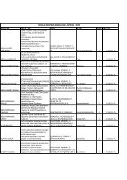
CD4027BC Dual J-K Master/Slave Flip-Flop with Set and Reset
CD4027BC Dual J-K Master/Slave Flip-Flop with Set and Reset
CD4027BC Dual J-K Master/Slave Flip-Flop with Set and Reset

Create successful ePaper yourself
Turn your PDF publications into a flip-book with our unique Google optimized e-Paper software.
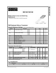
<strong>CD4027BC</strong><br />
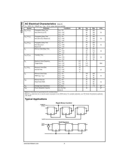
AC Electrical Characteristics (Note 8)<br />
T A = 25°C, C L = 50 pF, t rCL = t fCL = 20 ns, unless otherwise specified<br />
Symbol Parameter Conditions Min Typ Max Units<br />
t PHL or t PLH Propagation Delay Time V DD = 5V 200 400<br />
from Clock to Q or Q V DD = 10V 80 160 ns<br />
V DD = 15V 65 130<br />
t PHL or t PLH Propagation Delay Time V DD = 5V 170 340<br />
from <strong>Set</strong> to Q or <strong>Reset</strong> to Q V DD = 10V 70 140 ns<br />
V DD = 15V 55 110<br />
t PHL or t PLH Propagation Delay Time V DD = 5V 110 220<br />
from <strong>Set</strong> to Q or V DD = 10V 50 100 ns<br />
<strong>Reset</strong> to Q V DD = 15V 40 80<br />
t S Minimum Data <strong>Set</strong>up Time V DD = 5V 135 270<br />
V DD = 10V 55 110 ns<br />
V DD = 15V 45 90<br />
t THL or t TLH Transition Time V DD = 5V 100 200<br />
V DD = 10V 50 100 ns<br />
V DD = 15V 40 80<br />
f CL Maximum Clock Frequency V DD = 5V 2.5 5<br />
(Toggle Mode) V DD = 10V 6.2 12.5<br />
MHz<br />
V DD = 15V 7.6 15.5<br />
t rCL or t fCL Maximum Clock Rise V DD = 5V 15<br />
<strong>and</strong> Fall Time V DD = 10V 10<br />
µs<br />
V DD = 15V 5<br />
t W Minimum Clock Pulse V DD = 5V 100 200<br />
Width (t WH = t WL ) V DD = 10V 40 80 ns<br />
V DD = 15V 32 65<br />
t WH Minimum <strong>Set</strong> <strong>and</strong> V DD = 5V 80 160<br />
<strong>Reset</strong> Pulse Width V DD = 10V 30 60 ns<br />
V DD = 15V 25 50<br />
C IN Average Input Capacitance Any Input 5 7.5 pF<br />
C PD Power Dissipation Capacity Per <strong>Flip</strong>-<strong>Flop</strong> 35 pF<br />
(Note 9)<br />
Note 8: AC Parameters are guaranteed by DC correlated testing.<br />
Note 9: C PD determines the no load AC power consumption of any CMOS device. For complete explanation, see 74C Family Characteristics application<br />
note, AN-90.<br />
Typical Applications<br />
Ripple Binary Counters<br />
Shift Registers<br />
www.fairchildsemi.com 4