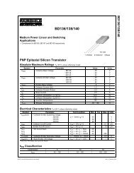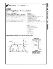
CD4027BC Dual J-K Master/Slave Flip-Flop with Set and Reset
CD4027BC Dual J-K Master/Slave Flip-Flop with Set and Reset
CD4027BC Dual J-K Master/Slave Flip-Flop with Set and Reset

You also want an ePaper? Increase the reach of your titles
YUMPU automatically turns print PDFs into web optimized ePapers that Google loves.
October 1987<br />
Revised March 2002<br />
<strong>CD4027BC</strong><br />
<strong>Dual</strong> J-K <strong>Master</strong>/<strong>Slave</strong> <strong>Flip</strong>-<strong>Flop</strong> <strong>with</strong> <strong>Set</strong> <strong>and</strong> <strong>Reset</strong><br />
General Description<br />
The <strong>CD4027BC</strong> dual J-K flip-flops are monolithic complementary<br />
MOS (CMOS) integrated circuits constructed <strong>with</strong><br />
N- <strong>and</strong> P-channel enhancement mode transistors. Each<br />
flip-flop has independent J, K, set, reset, <strong>and</strong> clock inputs<br />
<strong>and</strong> buffered Q <strong>and</strong> Q outputs. These flip-flops are edge<br />
sensitive to the clock input <strong>and</strong> change state on the positive-going<br />
transition of the clock pulses. <strong>Set</strong> or reset is<br />
independent of the clock <strong>and</strong> is accomplished by a high<br />
level on the respective input.<br />
All inputs are protected against damage due to static discharge<br />
by diode clamps to V DD <strong>and</strong> V SS .<br />
Ordering Code:<br />
Features<br />
■ Wide supply voltage range: 3.0V to 15V<br />
■ High noise immunity: 0.45 V DD (typ.)<br />
■ Low power TTL compatibility: Fan out of 2 driving 74L<br />
or 1 driving 74LS<br />
■ Low power: 50 nW (typ.)<br />
■ Medium speed operation: 12 MHz (typ.) <strong>with</strong> 10V<br />
supply<br />
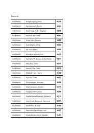
Order Number Package Number Package Description<br />
<strong>CD4027BC</strong>M M16A 16-Lead Small Outline Integrated Circuit (SOIC), JEDEC MS-012, 0.150" Narrow<br />
<strong>CD4027BC</strong>N N16E 16-Lead Plastic <strong>Dual</strong>-In-Line Package (PDIP), JEDEC MS-001, 0.300" Wide<br />
Devices also available in Tape <strong>and</strong> Reel. Specify by appending the suffix letter “X” to the ordering code.<br />
Connection Diagram<br />
Top View<br />
Truth Table<br />
CL<br />
(Note 3)<br />
Inputs t n−1<br />
(Note 1)<br />
Outputs t n<br />
(Note 2)<br />
J K S R Q Q Q<br />
I X O O O I O<br />
X O O O I I O<br />
O X O O O O I<br />
X I O O I O I<br />
X X O O X (No Change)<br />
X X X I O X I O<br />
X X X O I X O I<br />
X X X I I X I I<br />
I = HIGH Level<br />
O = LOW Level<br />
X = Don't Care<br />
= LOW-to-HIGH<br />
= HIGH-to-LOW<br />
Note 1: t n−1 refers to the time interval prior to the positive clock pulse<br />
transition<br />
Note 2: t n refers to the time intervals after the positive clock pulse<br />
transition<br />
Note 3: Level Change<br />
<strong>CD4027BC</strong> <strong>Dual</strong> J-K <strong>Master</strong>/<strong>Slave</strong> <strong>Flip</strong>-<strong>Flop</strong> <strong>with</strong> <strong>Set</strong> <strong>and</strong> <strong>Reset</strong><br />
© 2002 Fairchild Semiconductor Corporation DS005958 www.fairchildsemi.com
<strong>CD4027BC</strong><br />
Logic Diagram<br />
www.fairchildsemi.com 2
Absolute Maximum Ratings(Note 4)<br />
(Note 5)<br />
DC Supply Voltage (V DD )<br />
−0.5 V DC to +18 V DC<br />
Input Voltage (V IN )<br />
−0.5V to V DD +0.5 V DC<br />
Storage Temperature Range (T S ) −65°C to +150°C<br />
Power Dissipation (P D )<br />
<strong>Dual</strong>-In-Line<br />
700 mW<br />
Small Outline<br />
500 mW<br />
Lead Temperature (T L )<br />
(Soldering, 10 seconds) 260°C<br />
Recommended Operating<br />
Conditions (Note 5)<br />
DC Supply Voltage (V DD )<br />
3V to 15 V DC<br />
Input Voltage (V IN )<br />
0V to V DD V DC<br />
Operating Temperature Range (T A ) −55°C to +125°C<br />
Note 4: “Absolute Maximum Ratings” are those values beyond which the<br />
safety of the device cannot be guaranteed. They are not meant to imply<br />
that the devices should be operated at these limits. The table of “Recommended<br />
Operating Conditions” <strong>and</strong> “Electrical Characteristics” provides<br />
conditions for actual device operation.<br />
Note 5: V SS = 0V unless otherwise specified.<br />
<strong>CD4027BC</strong><br />
DC Electrical Characteristics (Note 6)<br />
Symbol Parameter Conditions<br />
−55°C +25°C +125°C<br />
Min Max Min Typ Max Min Max<br />
I DD Quiescent Device Current V DD = 5V, V IN = V DD or V SS 1 1 30<br />
V DD = 10V, V IN = V DD or V SS 2 2 60<br />
V DD = 15V, V IN = V DD or V SS 4 4 120<br />
V OL LOW Level |I O | < 1 µA<br />
Output Voltage V DD = 5V 0.05 0 0.05 0.05<br />
V DD = 10V 0.05 0 0.05 0.05<br />
V DD = 15V 0.05 0 0.05 0.05<br />
V OH HIGH Level |I O | < 1 µA<br />
Output Voltage V DD = 5V 4.95 4.95 5 4.95<br />
V DD = 10V 9.95 9.95 10 9.95<br />
V DD = 15V 14.95 14.95 15 14.95<br />
V IL LOW Level V DD = 5V, V O = 0.5V or 4.5V 1.5 1.5 1.5<br />
Input Voltage V DD = 10V, V O = 1V or 9V 3.0 3.0 3.0<br />
V DD = 15V, V O = 1.5V or 13.5V 4.0 4.0 4.0<br />
V IH HIGH Level V DD = 5V, V O = 0.5V or 4.5V 3.5 3.5 3.5<br />
Input Voltage V DD = 10V, V O = 1V or 9V 7.0 7.0 7.0<br />
V DD = 15V, V O = 1.5V or 13.5V 11.0 11.0 11.0<br />
I OL LOW Level Output V DD = 5V, V O = 0.4V 0.64 0.51 0.88 0.36<br />
Current (Note 7) V DD = 10V, V O = 0.5V 1.6 1.3 2.25 0.9<br />
V DD = 15V, V O = 1.5V 4.2 3.4 8.8 2.4<br />
I OH HIGH Level Output V DD = 5V, V O = 4.6V −0.64 −0.51 −0.88 −0.36<br />
Current (Note 7) V DD = 10V, V O = 9.5V −1.6 −1.3 −2.25 −0.9<br />
V DD = 15V, V O = 13.5V −4.2 −3.4 −8.8 −2.4<br />
I IN Input Current V DD = 15V, V IN = 0V −0.1 −10 −5 −0.1 −1.0<br />
V DD = 15V, V IN = 15V 0.1 10 −5 0.1 1.0<br />
Note 6: V SS = 0V unless otherwise specified.<br />
Note 7: I OH <strong>and</strong> I OL are tested one output at a time.<br />
Units<br />
µA<br />
V<br />
V<br />
V<br />
V<br />
mA<br />
mA<br />
µA<br />
3 www.fairchildsemi.com
<strong>CD4027BC</strong><br />
AC Electrical Characteristics (Note 8)<br />
T A = 25°C, C L = 50 pF, t rCL = t fCL = 20 ns, unless otherwise specified<br />
Symbol Parameter Conditions Min Typ Max Units<br />
t PHL or t PLH Propagation Delay Time V DD = 5V 200 400<br />
from Clock to Q or Q V DD = 10V 80 160 ns<br />
V DD = 15V 65 130<br />
t PHL or t PLH Propagation Delay Time V DD = 5V 170 340<br />
from <strong>Set</strong> to Q or <strong>Reset</strong> to Q V DD = 10V 70 140 ns<br />
V DD = 15V 55 110<br />
t PHL or t PLH Propagation Delay Time V DD = 5V 110 220<br />
from <strong>Set</strong> to Q or V DD = 10V 50 100 ns<br />
<strong>Reset</strong> to Q V DD = 15V 40 80<br />
t S Minimum Data <strong>Set</strong>up Time V DD = 5V 135 270<br />
V DD = 10V 55 110 ns<br />
V DD = 15V 45 90<br />
t THL or t TLH Transition Time V DD = 5V 100 200<br />
V DD = 10V 50 100 ns<br />
V DD = 15V 40 80<br />
f CL Maximum Clock Frequency V DD = 5V 2.5 5<br />
(Toggle Mode) V DD = 10V 6.2 12.5<br />
MHz<br />
V DD = 15V 7.6 15.5<br />
t rCL or t fCL Maximum Clock Rise V DD = 5V 15<br />
<strong>and</strong> Fall Time V DD = 10V 10<br />
µs<br />
V DD = 15V 5<br />
t W Minimum Clock Pulse V DD = 5V 100 200<br />
Width (t WH = t WL ) V DD = 10V 40 80 ns<br />
V DD = 15V 32 65<br />
t WH Minimum <strong>Set</strong> <strong>and</strong> V DD = 5V 80 160<br />
<strong>Reset</strong> Pulse Width V DD = 10V 30 60 ns<br />
V DD = 15V 25 50<br />
C IN Average Input Capacitance Any Input 5 7.5 pF<br />
C PD Power Dissipation Capacity Per <strong>Flip</strong>-<strong>Flop</strong> 35 pF<br />
(Note 9)<br />
Note 8: AC Parameters are guaranteed by DC correlated testing.<br />
Note 9: C PD determines the no load AC power consumption of any CMOS device. For complete explanation, see 74C Family Characteristics application<br />
note, AN-90.<br />
Typical Applications<br />
Ripple Binary Counters<br />
Shift Registers<br />
www.fairchildsemi.com 4
Physical Dimensions inches (millimeters) unless otherwise noted<br />
<strong>CD4027BC</strong><br />
16-Lead Small Outline Integrated Circuit (SOIC), JEDEC MS-012, 0.150" Narrow<br />
Package Number M16A<br />
5 www.fairchildsemi.com
<strong>CD4027BC</strong> <strong>Dual</strong> J-K <strong>Master</strong>/<strong>Slave</strong> <strong>Flip</strong>-<strong>Flop</strong> <strong>with</strong> <strong>Set</strong> <strong>and</strong> <strong>Reset</strong><br />
Physical Dimensions inches (millimeters) unless otherwise noted (Continued)<br />
16-Lead Plastic <strong>Dual</strong>-In-Line Package (PDIP), JEDEC MS-001, 0.300" Wide<br />
Package Number N16E<br />
Fairchild does not assume any responsibility for use of any circuitry described, no circuit patent licenses are implied <strong>and</strong><br />
Fairchild reserves the right at any time <strong>with</strong>out notice to change said circuitry <strong>and</strong> specifications.<br />
LIFE SUPPORT POLICY<br />
FAIRCHILD’S PRODUCTS ARE NOT AUTHORIZED FOR USE AS CRITICAL COMPONENTS IN LIFE SUPPORT<br />
DEVICES OR SYSTEMS WITHOUT THE EXPRESS WRITTEN APPROVAL OF THE PRESIDENT OF FAIRCHILD<br />
SEMICONDUCTOR CORPORATION. As used herein:<br />
1. Life support devices or systems are devices or systems<br />
which, (a) are intended for surgical implant into the<br />
body, or (b) support or sustain life, <strong>and</strong> (c) whose failure<br />
to perform when properly used in accordance <strong>with</strong><br />
instructions for use provided in the labeling, can be reasonably<br />
expected to result in a significant injury to the<br />
user.<br />
www.fairchildsemi.com 6<br />
2. A critical component in any component of a life support<br />
device or system whose failure to perform can be reasonably<br />
expected to cause the failure of the life support<br />
device or system, or to affect its safety or effectiveness.<br />
www.fairchildsemi.com