Dynamic Visualization of Antenna Patterns and Phased Array Beam ...
Dynamic Visualization of Antenna Patterns and Phased Array Beam ...
Dynamic Visualization of Antenna Patterns and Phased Array Beam ...

Create successful ePaper yourself
Turn your PDF publications into a flip-book with our unique Google optimized e-Paper software.
REPLACE THIS LINE WITH YOUR PAPER IDENTIFICATION NUMBER (DOUBLE-CLICK HERE TO EDIT) < 1<br />
<strong>Dynamic</strong> <strong>Visualization</strong> <strong>of</strong> <strong>Antenna</strong> <strong>Patterns</strong> <strong>and</strong><br />
<strong>Phased</strong> <strong>Array</strong> <strong>Beam</strong> Steering<br />
Brent Bauman, Student Member, IEEE, Andrew Christianson, Student Member, IEEE,<br />
Andrew Wegener, Student Member, IEEE, William J. Chappell, Member, IEEE<br />
<br />
Abstract—<strong>Antenna</strong> education is <strong>of</strong>ten hindered by the fact that<br />
radiation patterns are hard to visualize (RF electromagnetic<br />
waves are invisible) <strong>and</strong> require complicated, expensive<br />
equipment to measure. To solve this problem we have built a wall<br />
which illuminates when RF energy is directed at it. This allows<br />
immediate visualization <strong>of</strong> an antenna’s radiation pattern <strong>and</strong><br />
concepts such as wireless propagation, polarization, gain, <strong>and</strong><br />
even phased array beam steering. A low power LED rectenna<br />
array is used to create the visualization wall. We have also<br />
developed a multicolor LED rectenna which changes color<br />
depending on incident power. Also included is a phased array<br />
antenna with a crystal oscillator <strong>and</strong> power amplifier on the same<br />
board. This board allows the user to control the phase <strong>of</strong> signals<br />
fed to each <strong>of</strong> four columns <strong>of</strong> a 16 element patch array using only<br />
a rotary selector switch. This allows instructors to demonstrate<br />
the principles <strong>of</strong> phased array beam steering in real time all with<br />
a self contained system cost <strong>of</strong> less than $1500.<br />
(a)<br />
Index Terms—<strong>Antenna</strong> Competition 2010, rectenna,<br />
electronically steered array.<br />
A<br />
I. INTRODUCTION<br />
NTENNA education generally consists <strong>of</strong> theoretical <strong>and</strong><br />
mathematical demonstrations which result in polar plots<br />
<strong>of</strong> antenna gain. For a trained antenna engineer these plots are<br />
meaningful <strong>and</strong> are very useful in underst<strong>and</strong>ing a particular<br />
antenna’s performance. However, for beginners the plots are<br />
less than intuitive <strong>and</strong> are a real disconnect from an actual<br />
underst<strong>and</strong>ing <strong>of</strong> the radiation properties. Three dimensional<br />
polar plots available in s<strong>of</strong>tware packages like Ans<strong>of</strong>t HFSS<br />
have added a level <strong>of</strong> visualization but are still abstract to a<br />
novice. Furthermore, this difficulty in visualizing is not<br />
addressed by current measurement techniques which involve<br />
expensive <strong>and</strong> complicated equipment not to mention a need<br />
for an anechoic chamber – something not available at most<br />
high schools <strong>and</strong> even some universities. Even with this<br />
specialized equipment the visualization is delayed,<br />
Manuscript received May 1 2010.<br />
B. Bauman is with Purdue University, West Lafayette, IN, USA, 47907 (email:<br />
babauman@purdue.edu).<br />
A. Christianson is with Purdue University, West Lafayette, IN, USA,<br />
47907 (e-mail: christaj@purdue.edu).<br />
A. Wegener is with Purdue University, West Lafayette, IN, USA, 47907<br />
(e-mail: awegener@purdue.edu).<br />
W. J. Chappell is with Purdue University, West Lafayette, IN, USA, 47907<br />
(e-mail: chappell@purdue.edu).<br />
(b)<br />
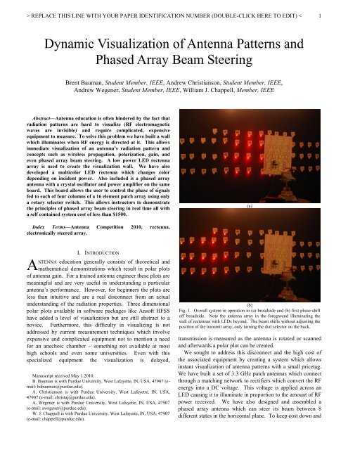
Fig. 1. Overall system in operation in (a) broadside <strong>and</strong> (b) first phase shift<br />
<strong>of</strong>f broadside. Note the antenna array in the foreground illuminating the<br />
wall <strong>of</strong> rectennas with LEDs beyond. The beam shifts without adjusting the<br />
position <strong>of</strong> the transmit array, only turning the dial selector on the back.<br />
transmission is measured as the antenna is rotated or scanned<br />
<strong>and</strong> afterwards a polar plot can be created.<br />
We sought to address this disconnect <strong>and</strong> the high cost <strong>of</strong><br />
the associated equipment by creating a system which allows<br />
instant visualization <strong>of</strong> antenna patterns with a small pricetag.<br />
We have built a set <strong>of</strong> 3.3 GHz patch antennas which connect<br />
through a matching network to rectifiers which convert the RF<br />
energy into a DC voltage. This voltage is applied across an<br />
LED causing it to illuminate in proportion to the amount <strong>of</strong> RF<br />
power received. We have also designed <strong>and</strong> assembled a<br />
phased array antenna which can steer its beam between 8<br />
different states in the horizontal plane. To keep cost down <strong>and</strong>
phase(phaseLargeBit..S(2,1))<br />
phase(phas<br />
S<br />
eM edium Bit..S(2,1))<br />
phase(phaseSm 21<br />
Phase (degrees)<br />
allBit..S(2,1))<br />
phase(S(2,1))<br />
> REPLACE THIS LINE WITH YOUR PAPER IDENTIFICATION NUMBER (DOUBLE-CLICK HERE TO EDIT) < 2<br />
allow even classrooms with no other RF equipment to use the<br />
system we generate the 3.3 GHz signal on a crystal oscillator<br />
then amplify it for transmission. That means the entire system<br />
is self contained <strong>and</strong> does not require any signal generator or<br />
other equipment. An example <strong>of</strong> the LED wall illuminated by<br />
our phased array antenna panel is shown in Fig. 1. The entire<br />
system is fabricated <strong>and</strong> populated by an external boardshop<br />
meaning that no special fabrication equipment or expertise is<br />
necessary for the user.<br />
As a side project we have developed a multicolor LED<br />
rectenna which changes color as a function <strong>of</strong> incident power.<br />
This <strong>of</strong>fers another level <strong>of</strong> visual interest to the LED wall <strong>and</strong><br />
could be especially helpful in capturing the attention <strong>of</strong><br />
younger students. This rectenna is not included in the final<br />
system price description but could be fabricated for minimal<br />
additional cost.<br />
We believe that either element <strong>of</strong> this system, the LED wall<br />
or the phased array panel would be useful to demonstrate<br />
antenna theory to all levels <strong>of</strong> student. Taken together they<br />
<strong>of</strong>fer a powerful demonstration system that will facilitate<br />
antenna education from the high school through graduate<br />
school level.<br />
II. DESIGN OF ANTENNA SYSTEM<br />
There are two devices in our system, an electronically<br />
scanned 16 element antenna array, <strong>and</strong> a set <strong>of</strong> antennas<br />
connected to rectifiers <strong>and</strong> LEDs. We will describe the design<br />
<strong>of</strong> each in the following subsections.<br />
A. Electronically Scanned <strong>Array</strong><br />
The 16 element patch antenna array is made on a 3 layer<br />
laminated board with Rogers 4350B dielectric. We used a<br />
0.79 mm board for the RF routing <strong>and</strong> circuitry. The center <strong>of</strong><br />
the board is nearly a solid ground plane with slots to feed the<br />
patch antennas on the opposite side which are 1.57 mm from<br />
the ground plane. This allows smaller lines on the routing freq side =<br />
due to the thinner substrate <strong>and</strong> efficient antennas on the other<br />
side due to the thicker substrate. Overall the array is 22.8 cm<br />
by 30.5 cm. The following subsections explain each <strong>of</strong> freq the =<br />
major components.<br />
signal generator capacity connected to other types <strong>of</strong> antennas,<br />
or as a phased array when the output is jumpered back onto the<br />
board into the RF distribution network.<br />
Phase Shifter<br />
We constructed a three bit delay line phase shifter. It was<br />
created on .030 inch Rogers 4350B (dielectric constant 3.66).<br />
We used four SPDT switches (PN: AS196-307LF) to switch<br />
between the three pairs <strong>of</strong> micro strip lines (see Figure 2b).<br />
Each curved delayed line provides a constant phase <strong>of</strong>fset<br />
over its straight line pair. Each pair corresponds to 1 bit. The<br />
smallest bit provides 45 o <strong>of</strong> phase shift, the medium bit<br />
provides 90 o <strong>of</strong> phase shift <strong>and</strong> the largest bit provides 180 o <strong>of</strong><br />
phase shift. Using combinations <strong>of</strong> these phase shifts any one<br />
<strong>of</strong> the four shifters can be set to have a phase <strong>of</strong> 0 to 270 o , in<br />
increments <strong>of</strong> 45 o , <strong>of</strong>fset from any other phase shifter.<br />
We use these shifters to set 8 states that provide smooth<br />
beam form steering. To achieve this one <strong>of</strong> the four shifters is<br />
permanently set in the in phase position. Though this phase<br />
shifter is essentially locked in place we still include the<br />
switches to ensure the phase through them <strong>and</strong> their loss is<br />
identical to the other rows.<br />
The first state sets all shifters to the in phase path. The<br />
second state sets each shifter +45 o <strong>of</strong>fset from its left most<br />
adjacent phase shifter. The third state than chooses each<br />
shifter to be +90 o <strong>of</strong>fset from its left most adjacent phase<br />
shifter. This continues with +45 o being added to the <strong>of</strong>fset for<br />
each subsequent state. Changing this phase <strong>of</strong>fset<br />
correspondingly alters the degree <strong>of</strong> max gain in relation to the<br />
patch antenna plane. Measured results <strong>of</strong> the phase shifter are<br />
shown in Fig. 2 which shows the difference in phase between<br />
the through state (“NoBitPhase”) <strong>and</strong> each <strong>of</strong> the other delay<br />
paths. The designed phase shifts are are 45 o , 90 o , <strong>and</strong> 180 o<br />
<strong>and</strong> measured shifts shown in Fig. 2 are 50.5 o , 92.4 o , <strong>and</strong><br />
178.7 o respectively. This level <strong>of</strong> accuracy is sufficient for a<br />
No B itP hase<br />
S ma llB itP ha se<br />
simple antenna demonstration unit.<br />
3.3 0 0GHz<br />
fre q= 3 .30 0 GHz<br />
p ha se (S (2 ,1))=5 9.8 74<br />
p ha se (pha seS m allB it..S (2 ,1 ))=9.4 00<br />
M ed iumB itP ha se<br />
3.3 0 0GHz<br />
p ha se (p hase Me d ium B it..S (2 ,1 ))=-3 2.5 7 7<br />
L a rg e B itP ha se<br />
fre q= 3 .30 0 GHz<br />
p ha se (pha seL arg eB it..S (2 ,1 ))=-11 8.8 6 9<br />
Voltage Controlled Oscillator<br />
The voltage controlled oscillator creates a 3.3 GHz signal<br />
with 1 dBm <strong>of</strong> output power. The chip is manufactured by<br />
Crystek <strong>and</strong> requires little circuitry to enable. The output is<br />
fed into an SMA connector to connect to the Power Amplifier.<br />
20 0<br />
10 0<br />
0<br />
N oB itP ha se<br />
S m a llB itP ha se<br />
Me dium B itP hase<br />
Amplifier<br />
We use the high power amplifier manufactured by RFMD<br />
(PN: SZM-3066ZSR). It is a 2 W amplifier that works from<br />
3.3-3.8Ghz. The amplifier is supplied <strong>and</strong> biased by a 5V DC<br />
power source that is also used for the digital logic biasing. It<br />
amplifies the 3.3GHz signal from the network analyzer to a<br />
34dBm output. The output <strong>of</strong> this amplifier is fed out <strong>of</strong> an<br />
SMA connector. This allows the array to function either in a<br />
-10 0<br />
-20 0<br />
L arg eB itP ha se<br />
2 .0 2.2 2.4 2. 6 2. 8 3.0 3.2 3.4 3 .6 3 .8 4.0<br />
F requency freq, GHz (G H z)<br />
Fig. 2. Measured reflection coefficient in dB as a function <strong>of</strong> frequency.<br />
Note the patch is closely matched to 50 at the design frequency <strong>of</strong> 3.3 GHz.
REPLACE THIS LINE WITH YOUR PAPER IDENTIFICATION NUMBER (DOUBLE-CLICK HERE TO EDIT) < 3<br />
2W<br />
R FM D<br />
PA<br />
C rystek<br />
V C O<br />
C ontrol Logic<br />
R otary<br />
S w itch<br />
R F Switch<br />
C ontrol<br />
Legend<br />
H L<br />
L H<br />
S M A<br />
C able<br />
W ilkinson<br />
P ow er<br />
D ividers<br />
50 <br />
50 <br />
S w itch C ontrol Lines<br />
(S w itches 1-12)<br />
1 2 3 4<br />
5 6 7 8<br />
50 <br />
50 <br />
50 <br />
9 10 11 12<br />
50 <br />
50 HL<br />
LH<br />
LH<br />
HL<br />
50 <br />
13 14 15 16<br />
4 3-bit Phase Shifters<br />
(a)<br />
Slot Fed Patch<br />
<strong>Antenna</strong><br />
<strong>Antenna</strong><br />
Layer<br />
(b)<br />
RO4350 (1.57 mm, 62 mil)<br />
Ground<br />
Plane<br />
RO4350 (0.79 mm, 31 mil)<br />
Routing<br />
Layer<br />
(c)<br />
Fig. 3. Electronically steered array (a) block diagram, (b) layout (red is routing layer, blue is ground plane (negative), <strong>and</strong> green is antenna layer), <strong>and</strong> (c)<br />
stackup.
Reflection Coefficient (dB)<br />
dB(s1_1)<br />
> REPLACE THIS LINE WITH YOUR PAPER IDENTIFICATION NUMBER (DOUBLE-CLICK HERE TO EDIT) < 4<br />
0<br />
-5<br />
-10<br />
-15<br />
-20<br />
-25<br />
-30<br />
2.0 2.2 2.4 2.6 2.8 3.0 3.2 3.4 3.6 3.8 4.0<br />
freq, GH z<br />
Multi Layer Patch <strong>Antenna</strong><br />
We designed a slot fed patch antenna with HFSS before<br />
building <strong>and</strong> testing it on a laminated 30 <strong>and</strong> 60 mil Rogers<br />
4350B board. The antenna uses a slot coupling method that<br />
maximizes the H field in the slot by allowing an approximately<br />
/4 open stub past the slot <strong>and</strong> matches the antenna to 50 .<br />
One <strong>of</strong> the sixteen patch antennas is indicated in Fig. 3b. The<br />
antenna has a measured reflection coefficient <strong>of</strong> -27 dB as<br />
shown in Fig. 4 <strong>and</strong> an efficiency <strong>of</strong> approximately 79% as<br />
simulated in HFSS.<br />
Phase Shifter Control Logic<br />
The control logic is used to bridge the gap between the user<br />
input (rotary switch) <strong>and</strong> the proper biasing states <strong>of</strong> the 16<br />
SPDTs. Since each switch requires two control pins, a low<br />
<strong>and</strong> a high, we needed a custom decoder <strong>and</strong> 2 hex inverters.<br />
We settled on a Gal26cv12B PLD. The control program<br />
designed for this chip uses a simple lookup table that takes the<br />
state <strong>of</strong> the 8 pins from the rotary switch <strong>and</strong> converts them to<br />
the appropriate 12 states. These 12 outputs are than run to 12<br />
inverters <strong>and</strong> one pin on each SPDT on three <strong>of</strong> the phase<br />
shifters. Each <strong>of</strong> the inverter outputs is then run the second pin<br />
on the 12 SPDTs. The DC lines run between the rotary switch<br />
the PLD, to the inverters, to the SPDTs. They are kept away<br />
from RF lines <strong>and</strong> the antennas themselves <strong>and</strong> isolated from<br />
RF path by capacitors where necessary.<br />
The PLD is available for purchase from Dataman<br />
preprogrammed for $39.27 as indicated in Table II. Many<br />
universities have PLDs on h<strong>and</strong> <strong>and</strong> the capability in house to<br />
program them. This capability could reduce or remove the<br />
cost <strong>of</strong> this component from the system. Table I lists the<br />
connections made by the PLD.<br />
Overall Design<br />
The overall layout <strong>of</strong> the RF subsystems is very important.<br />
All separate RF lines before <strong>and</strong> after the phase shifter need to<br />
be <strong>of</strong> equal length so the only phase added to the line comes<br />
from the phase shifter.<br />
We chose Wilkinson power dividers to provide power<br />
splitting because these are a simple way to split power with<br />
low reflection <strong>and</strong> even phase response.<br />
m1<br />
Frequency (G H z)<br />
m1<br />
freq= 3.300 GHz<br />
dB (s1 _1)=-2 7.0 20<br />
V alle y<br />
Fig. 4. Measured reflection coefficient in dB as a function <strong>of</strong> frequency.<br />
Note the patch is closely matched to 50 at the design frequency <strong>of</strong> 3.3 GHz.<br />
TABLE I<br />
LOGIC CONTROL LINE CONNECTIONS<br />
PLD Pin # Pin Connections<br />
Pin 1<br />
Gnd<br />
Pin 2<br />
Gnd<br />
Pin 3<br />
Gnd<br />
Pin 4<br />
Gnd<br />
Pin 5<br />
Gnd<br />
Pin 6 Rotary Switch Pin #1<br />
Pin 7<br />
Pwr (+5V)<br />
Pin 8 Rotary Switch Pin #2<br />
Pin 9 Rotary Switch Pin #3<br />
Pin 10 Rotary Switch Pin #4<br />
Pin 11 Rotary Switch Pin #5<br />
Pin 12 Rotary Switch Pin #6<br />
Pin 13 Rotary Switch Pin #7<br />
Pin 14 Rotary Switch Pin #8<br />
Pin 15 V1 <strong>of</strong> SPDT #3<br />
Pin 16 V1 <strong>of</strong> SPDT #4<br />
Pin 17 V1 <strong>of</strong> SPDT #6<br />
Pin 18 V1 <strong>of</strong> SPDT #7<br />
Pin 19 V1 <strong>of</strong> SPDT #8<br />
Pin 20 V1 <strong>of</strong> SPDT #12<br />
Pin 21<br />
Gnd<br />
Pin 22 V1 <strong>of</strong> SPDT #5<br />
Pin 23 V1 <strong>of</strong> SPDT #1<br />
Pin 24 V1 <strong>of</strong> SPDT #2<br />
Pin 25 V1 <strong>of</strong> SPDT #11<br />
Pin 26 V1 <strong>of</strong> SPDT #10<br />
Pin 27 V1 <strong>of</strong> SPDT #9<br />
Pin 28<br />
Gnd<br />
B. LED Rectenna Module<br />
The LED Rectenna array is made <strong>of</strong> 70 small 41.6mm x<br />
54.1mm tag boards displayed on a backing board. This tag is<br />
made <strong>of</strong> three main entities, a 3.3GHz single layer patch<br />
antenna, a matching network, <strong>and</strong> a voltage boosting rectifier<br />
with LED. This device takes a polarized 3.3GHz signal <strong>and</strong><br />
turns it into visual light.<br />
Single Layer Patch <strong>Antenna</strong><br />
We designed a single layer patch antenna on 1.57 mm thick<br />
Rogers RO4350B. The antenna is designed to be matched to<br />
50 ohms by adjusting the depth that the 50 ohm microstrip line<br />
penetrates it.<br />
Rectifier/LED<br />
The rectifier is a four stage charge pump that uses four<br />
Schottky diodes <strong>and</strong> four capacitors. The load is a low power<br />
LED with a low turn on voltage.<br />
We used a charge pump to provide voltage boost to the<br />
LED to increase the rectified voltage above the turn on voltage<br />
<strong>of</strong> the LED (see Fig. 5a). Adding more stages increases the<br />
DC voltage output, however losses also increase degrading<br />
performance. We balanced these effects <strong>and</strong> chose a 4 stage<br />
rectifier.<br />
Matching Network<br />
A matching network is used to provide maximum power<br />
transfer from the antenna to the rectifier with the low power<br />
LED load.<br />
To implement the matching network we utilize microstrip
REPLACE THIS LINE WITH YOUR PAPER IDENTIFICATION NUMBER (DOUBLE-CLICK HERE TO EDIT) < 5<br />
Transmit<br />
<strong>Array</strong><br />
(a)<br />
Multicolor<br />
Patch<br />
Farthest - Red<br />
Multicolor<br />
Patch<br />
(a)<br />
Transmit <strong>Array</strong><br />
Transmit <strong>Array</strong><br />
(b)<br />
Closer - Purple<br />
Multicolor<br />
Patch<br />
<strong>Antenna</strong><br />
Layer<br />
(b)<br />
RO4350 (1.57 mm, 62 mil)<br />
Ground<br />
Plane<br />
(c)<br />
Fig. 5. Rectenna (a) schematic <strong>and</strong> (b) layout (red is routing layer, blue is<br />
ground plane (negative), <strong>and</strong> green is antenna layer), <strong>and</strong> (c) stackup.<br />
lines <strong>and</strong> series inductors. There is a short length <strong>of</strong> line<br />
leading away from the rectifier followed by a 5.6 nH inductor,<br />
another length <strong>of</strong> line, <strong>and</strong> a 2.2 nH inductor.<br />
Closest - Green<br />
(c)<br />
Fig. 6. Multi-color LED demonstration. Increasing power changes tag color<br />
from (a) red to (b) purple to (c) green.<br />
Multicolor Rectenna<br />
We also have created a multicolor rectenna which uses 3<br />
LEDs in a single package, red, green, <strong>and</strong> blue (Digikey PN:<br />
350-2096-1-ND, $2.17 each). The circuit is laid out to<br />
balance the brightness <strong>of</strong> the LEDs. Due to their different turn<br />
on voltages different colors illuminate at different incident RF<br />
Power levels. This is shown in Fig. 6. Although illuminating<br />
the blue <strong>and</strong> green LEDs requires the transmitter to be close to<br />
the wall for sufficient power the red LED still illuminates at a<br />
distance with little loss in sensitivity compared to the single<br />
color rectenna. If so desired this design may be slightly higher<br />
cost option for interested schools.<br />
III. PHOTOS OF COMPLETED SYSTEM<br />
Figure 7 shows a photograph <strong>of</strong> a completed rectenna tag.<br />
Fig. 7 Completed rectenna tag
REPLACE THIS LINE WITH YOUR PAPER IDENTIFICATION NUMBER (DOUBLE-CLICK HERE TO EDIT) < 6<br />
(a)<br />
Fig. 8 Completed transmit phased array. (a) Routing layer (0.79 mm thick) <strong>and</strong> (b) antenna layer (1.57 mm thick).<br />
Figure 8 shows the completed transmit array panel front <strong>and</strong><br />
back. The array clearly has some manual wire jumpers which<br />
will need to be installed by the end user. These were<br />
necessary for DC routing in order to avoid another board layer<br />
which would have made the manufacturing significantly more<br />
expensive. Also the array shown does not have the an<br />
integrated oscillator <strong>and</strong> amplifier. These subsystems are still<br />
<strong>of</strong>f panel at this point but will be placed in the lower right<br />
section <strong>of</strong> the board where the DC supply currently is (see Fig.<br />
8a).<br />
IV. ASSEMBLY AND OPERATION INSTRUCTIONS<br />
Because we have <strong>of</strong>floaded the manufacturing to an external<br />
board house very little assembly is required. To reduce cost<br />
we have purchased our own parts from various vendors such as<br />
Digikey <strong>and</strong> procured free substrate from Rogers through their<br />
university sample program [1]. We also found a board<br />
manufacturer, Electronic Interconnect, which allows the user<br />
to supply their own board which they then process [2]. As<br />
mentioned previously there will be 4 jumper connections<br />
which will need to be soldered by the end user. These will be<br />
simple connections easily completed by a novice solderer <strong>and</strong><br />
are necessary to keep the board 3 layers, critical to keeping<br />
(b)<br />
board manufacturing cost down.<br />
Assembly starts by ordering all components needed for this<br />
project (see Table II). The PLD needs to be ordered from<br />
Dataman with our VHDL program already copied onto the<br />
chip. Substrate can be obtained free by educational<br />
institutions from Rogers [1]. Once the parts are obtained they<br />
can be sent for ably at a board house.<br />
After fabrication <strong>of</strong> the boards it will be necessary to mount<br />
the rectennas to something. We have had success with foam<br />
core board <strong>and</strong> double stick tape. For a more reconfigurable<br />
setup a felt sheet <strong>and</strong> self adhesive Velcro on the rectennas is<br />
also possible.<br />
V. SAMPLE LESSONS<br />
A. Wireless Power Transmission<br />
Transmitting power from one point in the room to another,<br />
especially in an amount sufficient to illuminate an LED, may<br />
be the first concrete illustration <strong>of</strong> electromagnetic waves for<br />
high school level students. This lesson would focus on a<br />
qualitative underst<strong>and</strong>ing <strong>of</strong> electromagnetic fields <strong>and</strong> how<br />
they propagate. More advanced lessons may include<br />
derivations beginning with Maxwell’s equations all the way<br />
through Friis’ transmission equation.
REPLACE THIS LINE WITH YOUR PAPER IDENTIFICATION NUMBER (DOUBLE-CLICK HERE TO EDIT) < 7<br />
Fig. 9 Screen capture <strong>of</strong> Mathematica Player program for dynamically<br />
visualing array patterns. There is a brief description followed by a diagram<br />
describing the problem <strong>and</strong> finally the interactive antenna array plot.<br />
B. <strong>Beam</strong> Shape<br />
The pattern <strong>of</strong> the antenna when all antennas are fed with<br />
uniform phase will be round as observed on the rectenna array.<br />
This lesson could start with the pattern <strong>of</strong> a single patch, <strong>and</strong><br />
then progress to underst<strong>and</strong>ing the array factor which will<br />
increase gain as the effective antenna area increases. Using<br />
the transmit antenna array the concept could be demonstrated<br />
by masking some <strong>of</strong> the array elements with aluminum foil <strong>and</strong><br />
observing the effect on beam shape (one antenna gives a larger<br />
beam width; a row will give an oblong shape).<br />
C. Polarization Effects<br />
When the transmit antenna is rotated 90 o from the receive<br />
array the antennas will be cross-polarized. This results in<br />
minimal power being absorbed by the rectennas; thus the<br />
LEDs will not be turned on. By rotating the transmit array to<br />
bring it back into the same polarization as the receive array,<br />
the LEDs relight. The lesson taught about this effect can<br />
explain polarization in a practical way, illustrating its<br />
importance as an antenna design consideration as opposed to<br />
simply using vector math to illustrate that the antennas will not<br />
transmit power from one to the other.<br />
D. <strong>Beam</strong> Steering<br />
This lesson could explore the fundamentals <strong>of</strong> electronic<br />
beam steering with a discussion <strong>of</strong> the effect <strong>of</strong> feeding each<br />
element with a different phase <strong>of</strong> current. Calculations such as<br />
these are frequently done in the undergraduate microwave<br />
engineering class at our university, but are not reinforced with<br />
experiment due to the complexity involved in phased array<br />
antenna design <strong>and</strong> fabrication. Our supplied system provides<br />
a way around that to allow real time visual underst<strong>and</strong>ing <strong>of</strong><br />
the affect <strong>of</strong> phase shift on an antenna array’s pattern. The<br />
transmit antenna array will have a rotary knob allowing<br />
selection <strong>of</strong> one <strong>of</strong> 8 phase shift states. This will allow the<br />
beam to steer to 8 positions indicated by a different set <strong>of</strong> LED<br />
lights being illuminated at each stage. To supplement this<br />
lesson as promised in the proposal we developed a program<br />
which allows real time calculation <strong>and</strong> display <strong>of</strong> antenna array<br />
patterns with sliders to allow the user to control both spacing<br />
<strong>and</strong> phase shift across the array. The program is implemented<br />
using Mathematica <strong>and</strong> can be used by anyone with the freely<br />
downloadable Mathematica Player [3]. The program is<br />
available<br />
here:<br />
http://www.wolfram.com/solutions/interactivedeployment/publ<br />
ish/download.jsp?id=0852331133&filename=<strong>Antenna</strong><strong>Array</strong>Vi<br />
sualization.nbp until May 15, 2010 or from the authors upon<br />
request. Fig. 9 shows a screen shot <strong>of</strong> the program.<br />
E. Patch <strong>Antenna</strong> Theory<br />
Both the receive array <strong>and</strong> transmit array are made up <strong>of</strong><br />
patch antennas. This lesson would teach the fundamentals <strong>of</strong><br />
patch antenna design, including resonant modes <strong>and</strong> coupling<br />
mechanisms. In underst<strong>and</strong>ing this lesson, the physics behind<br />
the polarization demonstration will be brought out as well as<br />
an underst<strong>and</strong>ing <strong>of</strong> the beam shape <strong>of</strong> a single patch antenna.<br />
It should be noted that the system incorporates both a slot fed<br />
3 layer patch antenna <strong>and</strong> a 2 layer microstrip line patch<br />
antenna. This allows a more general underst<strong>and</strong>ing <strong>of</strong><br />
coupling structures as the class will be provided with to<br />
demonstrations <strong>of</strong> how to properly couple an antenna.<br />
F. Matching Networks<br />
The rectennas have a mixed lumped element/transmission<br />
line matching network to match the antennas to the input <strong>of</strong> the<br />
rectifier. This lesson would be a follow up to a series on<br />
underst<strong>and</strong>ing input impedance <strong>and</strong> Smith Charts. With that<br />
underst<strong>and</strong>ing the student would be able to infer the<br />
impedance looking into the rectenna’s rectifier knowing the<br />
boards layout <strong>and</strong> inductor values. Furthermore they could<br />
alter the matching network by placing other components or<br />
simply shorting the inductors <strong>and</strong> view the importance <strong>of</strong><br />
matching as the sensitivity <strong>of</strong> the mismatched patch drops<br />
precipitously. If so desired we could provide information<br />
about rectifier input impedance to be used in example<br />
calculations.<br />
VI. LIST OF PARTS<br />
The parts necessary to assemble the system are listed in<br />
Table II. This includes information about suppliers <strong>and</strong> cost as<br />
well as hyperlinks to datasheets where applicable.<br />
VII. CONCLUSION<br />
<strong>Antenna</strong> education has until now lacked a mechanism for<br />
instant feedback <strong>and</strong> visualization <strong>of</strong> antenna properties that<br />
will both excite <strong>and</strong> instruct students. We believe that the<br />
LED rectenna wall we have developed addresses that problem<br />
with a dynamic, real time mechanism for visualizing <strong>and</strong><br />
underst<strong>and</strong>ing antenna patterns. Furthermore, the phased array<br />
panel portion will introduce this exciting technology to all<br />
levels from high school students through graduate students.
REPLACE THIS LINE WITH YOUR PAPER IDENTIFICATION NUMBER (DOUBLE-CLICK HERE TO EDIT) < 8<br />
We believe the combination <strong>of</strong> these two components will<br />
serve as a powerful tool for recruiting <strong>and</strong> educating the next<br />
generation <strong>of</strong> antenna engineers.<br />
http://rogerscorp.com/acm/forms/form_university.aspx.<br />
[2] Electronic Interconnect, Available: http://www.eiconnect.com/.<br />
[3] Wolfram Research Inc., Wolfram Mathematica Player. Available:<br />
http://www.wolfram.com/products/player/download.cgi .<br />
REFERENCES<br />
[1] Rogers Corporation, University Program, Available:<br />
Item<br />
Part Number<br />
Brent Bauman is a Senior in electrical <strong>and</strong> computer engineering at Purdue<br />
University. He has accepted a job after graduation at the Crane Naval<br />
Surface Warfare Center in Crane, IN working with the Navy’s electronic<br />
TABLE II<br />
COMPONENT LIST/BUDGET<br />
Distributor’s<br />
Part Number<br />
Distributor Qty. Price Ea.<br />
($)<br />
Total<br />
Price ($)<br />
RECTENNA BOARDS<br />
2.2nH Inductor IMC0603ER2N2S 70-IMC0603ER2N2S Mouser 70 0.15 10.50<br />
5.6nH Inductor IMC0603ER5N6J 70-IMC0603ER5N6J Mouser 70 0.15 10.50<br />
64pF Capacitor GRM1885C1H620FA01D 81-GRM185C1H620FA01D Mouser 280 0.15 42.00<br />
Schottky Diode SMS7630-005LF SMS7630-005LF RFMW 140 0.74 103.60<br />
LED sml-211utt86 511-1292-1-ND Digikey 140 0.17 23.80<br />
PCB Assembly 70 8.00 560.00<br />
ELECTRONICALLY SCANNED ARRAY<br />
50 ohm resistors CRCW0603100RFKEA 71-CRCW0603-50-E3 Mouser 32 0.014 0.45<br />
100 ohm resistors CRCW0603100RFKEA 652-CR0603-JW-101ELF Mouser 15 0.03 0.45<br />
81-<br />
7.5pf capacitors GRM1885C1H7R5DZ01D GRM185C1H7R5DZ01D Mouser 80 0.06 4.80<br />
1.1k ohm resistors ERJ-2RKF1101X P1.10KLCT-ND Digikey 10 .098 .98<br />
4.02k ohm resistors ERJ-2RKF4021X P4.02KLCT-ND Digikey 10 .098 .98<br />
825 ohm resistor CRCW0402825RFKED 541-825LCT-ND Digikey 10 .083 .83<br />
2.74k ohm resistor ERJ-2RKF2741X P2.74KLCT-ND Digikey 10 .098 .83<br />
47k ohm resistor ERJ-2RKF4702X P47.0KLCT-ND Digikey 10 .098 .98<br />
3k ohm resistor CRCW04023K00FKED 541-3.00KLCT-ND Digikey 10 .083 .83<br />
1 uF capacitor 1206YC105JAT2A 478-5178-1-ND Digikey 10 1.089 10.89<br />
3.9 pF capacitor UVK105CH3R9JW-F 587-1021-1-ND Digikey 10 .165 1.65<br />
.1 uF capacitor C0402C104K8PACTU 399-3027-1-nd Digikey 10 .024 .24<br />
6.2 nH inductor LQW15AN6N2D00D 490-1141-1-ND Digikey 10 .818 3.18<br />
4.7 nH inductor LQW18AN4N7D00D 490-1162-1-ND Digikey 10 .329 3.29<br />
1.5 pF capacitor C0402C159C5GACTU 399-1002-1-ND Digikey 10 .061 .61<br />
10 pF capacitor 04025U100FAT2A 478-5717-1-ND Digikey 10 .419 4.19<br />
High Power Amplifier SZM-3066ZSR 25R5121 Newark 1 19.98 19.98<br />
Voltage Controlled<br />
Oscillator CVCO55BE-3206-3306 393-0116<br />
Allied<br />
Electronics 1 16.39 16.39<br />
.031” Board mount SMA<br />
connector 142-0701-881 J657-ND Digikey 2 9.63 19.26<br />
SPDT Switch AS218-321LF 863-1010-1-ND Digikey 16 1.12 17.92<br />
IC Hex Inverter 296-1630-5-ND Digikey 2 0.62 1.24<br />
Programmable Logic<br />
Device (Preprogrammed) GAL26V12B N/A Dataman 1 39.27 39.27*<br />
Rotary Switch<br />
(8 position) 50DP45-01-1-AJN GH7353-ND Digikey 1 17.17 17.17<br />
5 volt Power Supply 709-GS60A05-P1J Mouser 1 44.00 44.00<br />
PCB Assembly 1 425.00 425.00<br />
ACCESSORIES<br />
12” SMA Cable CCSMA-MM-RG316DS-12 744-1276-ND Digikey 1 14.87 14.87<br />
TOTAL COST $1400.68<br />
*The PLD will be much cheaper if the users have PLD programming capability as most universities do.
REPLACE THIS LINE WITH YOUR PAPER IDENTIFICATION NUMBER (DOUBLE-CLICK HERE TO EDIT) < 9<br />
warfare <strong>and</strong> radar systems.<br />
Andrew Christianson is a fifth year PhD student in electrical <strong>and</strong> computer<br />
engineering at Purdue University. He has accepted a job after graduation at<br />
the Crane Naval Surface Warfare Center in Crane, IN working with the<br />
Navy’s electronic warfare systems.<br />
His primary research is in passive intermodulation distortion specifically<br />
techniques for measuring <strong>and</strong> mitigating it.<br />
Andrew Wegener is a third year PhD student in electrical <strong>and</strong> computer<br />
engineering at Purdue University.<br />
His primary research is novel packaging techniques for high power<br />
components with a focus on creating cheap, high performance phased array<br />
systems.<br />
William Chappell is an asoociate pr<strong>of</strong>essor in electrical <strong>and</strong> computer<br />
engineering at Purdue University.<br />
His primary research is novel packaging techniques for high power<br />
components with a focus on creating cheap, high performance phased array<br />
systems.