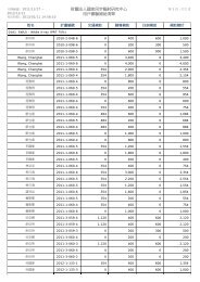
conduction emi and emc measurement and testing in nsrrc power ...
conduction emi and emc measurement and testing in nsrrc power ...
conduction emi and emc measurement and testing in nsrrc power ...

Create successful ePaper yourself
Turn your PDF publications into a flip-book with our unique Google optimized e-Paper software.
STANDARD DIAGRAM<br />
We tested correction <strong>power</strong> supply <strong>and</strong> only<br />
<strong>in</strong>spected the current long-term stability (8 hours) <strong>and</strong><br />
low span current ripple (0kHz to 1kHz) for st<strong>and</strong>ard<br />
confirmation <strong>in</strong> TLS, but never to verify the high<br />
frequency noise of the AC to DC voltage <strong>power</strong> supply.<br />
The st<strong>and</strong>ard diagram of FCC Part 15 <strong>and</strong> VDE 0871 is<br />
<strong>in</strong>dicated <strong>in</strong> the figure 4. The <strong>measurement</strong> frequency is<br />
from 9kHz to 30 MHz. The figure 4 is FCC Part 15 <strong>and</strong><br />
VDE 0871 with frequency diagram.<br />
the fly-back converter. We can flow D.M. path <strong>and</strong> C.M.<br />
path to f<strong>in</strong>d the noise source <strong>and</strong> coupl<strong>in</strong>g Pathes.<br />
If the voltage converter <strong>power</strong> supply had followed<br />
the detail to design, its nosice will be <strong>in</strong> to the<br />
specification <strong>and</strong> no noise to <strong>in</strong>terfere the other <strong>power</strong><br />
supply.<br />
Figure 6: The noise source <strong>and</strong> coupl<strong>in</strong>g Path.<br />
Figure 4: FCC Part 15 <strong>and</strong> VDE 0871 with frequency<br />
diagram.<br />
We expect the <strong>power</strong> supply add the FCC st<strong>and</strong>ard<br />
<strong>test<strong>in</strong>g</strong> <strong>and</strong> put <strong>measurement</strong> <strong>in</strong> the future. For example,<br />
TPS <strong>power</strong> supply must be fulfilled the requirement of<br />
the st<strong>and</strong>ard.<br />
CONDUCTED EMI TESTING<br />
In the first section,we must adjust the <strong>measurement</strong><br />
for resolution b<strong>and</strong>width (RBW) from 9KHz to<br />
150KHz,<strong>and</strong> the RBW is sett<strong>in</strong>g 200 Hz. The second<br />
section is from 150 KHz to 30 MHz, <strong>and</strong> the RBW is<br />
settimg 9 KHz.<br />
Refer to Figure 7, it shows I DM which is differential<br />
mode current path. Figure 8 <strong>in</strong>dicates I CM which is the<br />
common mode ground current path.<br />
Figure 7: The differential mode current path I DM<br />
Figure 8: The common mode current path I CM.<br />
Figure 5: Indicates the LISN component of<br />
decomposed diagram.<br />
The detail of LISN is showed <strong>in</strong> figure 2 with load. We<br />
can exquisite to decompose the LISN component as<br />
figure 5.<br />
NOISE SOURCES<br />
The coupl<strong>in</strong>g Pathes of the D.M. Noise comes from<br />
current(i) while the C.M. Noise caused by Parasitic<br />
Capacitances. Therefore, we must reduce current(i) <strong>and</strong><br />
the Parasitic capacitances. The Figure 6 shows the noise<br />
source <strong>and</strong> coupl<strong>in</strong>g Path. The diagram is <strong>in</strong>put stage of<br />
TESTING AND RESULT<br />
Compar<strong>in</strong>g to Figure 4, we can separate the FCC<br />
Class A Part 15 stantard to four sections for mursement.<br />
The section 1 is from 9kHz to 150kHz. The section two<br />
is from 150kHz to 450kHz. The The section three is<br />
from 450kHz to 1.6MHz. The The section four is from<br />
1.6MHz to 30 MHz.<br />
We can confim the noise from figure 10 to figure 12.<br />
All the noise should be fullfilled the st<strong>and</strong>ard of FCC<br />
Class A Part 15 st<strong>and</strong>ard <strong>and</strong> VDE 0871A. As the result,<br />
the noise can’t reach to FCC Class A Part 15 st<strong>and</strong>ard<br />
<strong>and</strong> VDE 0871A. But only the figure 9 show the noise<br />
spectrum can’t pass FCC Class A Part 15 st<strong>and</strong>ard frist<br />
section. We design <strong>and</strong> add<strong>in</strong>g a filter put <strong>in</strong> <strong>power</strong><br />
supply, thus frist section can pass FCC Class A Part 15<br />
st<strong>and</strong>ard as figure 13.