conduction emi and emc measurement and testing in nsrrc power ...
conduction emi and emc measurement and testing in nsrrc power ...
conduction emi and emc measurement and testing in nsrrc power ...

You also want an ePaper? Increase the reach of your titles
YUMPU automatically turns print PDFs into web optimized ePapers that Google loves.
CONDUCTION EMI AND EMC MEASURE AND TEST POWER SUPPLY IN<br />
NSRRC<br />
Chen-Yao Liu, Yung-Hui, Liu<br />
National Synchrotron Radiation Research Center, Hs<strong>in</strong>chu, 30076, Taiwan<br />
Abstract<br />
The correction <strong>power</strong> supplies are work<strong>in</strong>g <strong>in</strong> the<br />
storage r<strong>in</strong>g of NSRRC. They are required to output<br />
high quality <strong>and</strong> high performance current that is<br />
long-term stability <strong>and</strong> output current ripple are required<br />
to be under 100ppm. The storage r<strong>in</strong>g consists of more<br />
than one hundred units of <strong>in</strong>dependence <strong>power</strong> supplies<br />
work<strong>in</strong>g together when beam current <strong>in</strong> 1.5GeV status.<br />
The <strong>power</strong> supplies also are all work<strong>in</strong>g under current<br />
mode. We just build a new <strong>conduction</strong> EMI<br />
(Electromagnetic Interference) <strong>and</strong> EMC<br />
(Electromagnetic Compatibility) <strong>measurement</strong><br />
laboratory to measure <strong>and</strong> test the switch<strong>in</strong>g <strong>power</strong><br />
supplies. That is AC to DC voltage bus source to supply<br />
for the switch<strong>in</strong>g correction <strong>power</strong> supply. Us<strong>in</strong>g the<br />
LISN to obta<strong>in</strong> <strong>conduction</strong> noise, it is high frequency<br />
voltage noise generated by the switch<strong>in</strong>g mode of <strong>power</strong><br />
supply <strong>conduction</strong> noise. The current signal pass AC<br />
source impendence stabilize network LISN <strong>and</strong><br />
spectrum analyzer will obta<strong>in</strong> the <strong>conduction</strong> noise. We<br />
can use a noise separator to separate common EMI noise<br />
<strong>and</strong> difference-mode EMI noise for EMI filter<strong>in</strong>g design.<br />
The <strong>measurement</strong> result will be illustrated <strong>in</strong> the paper.<br />
INTRODUCTION<br />
A LISN is used to ensure repeatable EMI <strong>and</strong> EMC<br />
<strong>measurement</strong> <strong>power</strong> frequency signal pass<strong>in</strong>g through<br />
LISN <strong>and</strong> LISN is not unaffected. It can fix the AC<br />
source l<strong>in</strong>e impedance network, so we call l<strong>in</strong>e<br />
impedance stabiliz<strong>in</strong>g network (LISN).<br />
Equipment is very important for noice mesurment<br />
showed as figure 1. That <strong>in</strong>dicates the lab Equipment<br />
under test the connection of LISN diagram.<br />
The st<strong>and</strong>er EUT is required to pass the environment<br />
for FCC or VDE <strong>measurement</strong> specification for EMI<br />
<strong>and</strong> EMC noise test.<br />
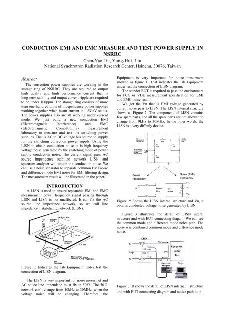
We get the Vn that is EMI voltage generated by<br />
current noise pass to LISN. The LISN <strong>in</strong>ternal structure<br />
shows as Figure 2. The component of LISN conta<strong>in</strong>s<br />
few spare parts, <strong>and</strong> all the spare parts are not allowed to<br />
change from 9kHz to 30MHz. In the other words, the<br />
LISN is a very diffculy device.<br />
Figure 2: Shows the LISN <strong>in</strong>ternal structure <strong>and</strong> Vn, it<br />
obta<strong>in</strong>s conducted voltage noise generated by LISN.<br />
Figure 3 illustrates the detail of LISN <strong>in</strong>teral<br />
structure <strong>and</strong> with EUT connect<strong>in</strong>g diagam. We can see<br />
the common mode <strong>and</strong> differenct mode noice path. The<br />
noise was comb<strong>in</strong>ed common mode <strong>and</strong> difference mode<br />
noise.<br />
Figure 1: Indicates the lab Equipment under test the<br />
connection of LISN diagram.<br />
The LISN is very important for noise mesurmet <strong>and</strong><br />
AC souce l<strong>in</strong>e impendanc must fix <strong>in</strong> 50Ω. The 50Ω<br />
network can’t change from 10kHz to 30MHz, when the<br />
voltage noice will be chang<strong>in</strong>g. Therefore, the<br />
Figure 3: It shows the detail of LISN <strong>in</strong>ternal structure<br />
<strong>and</strong> with EUT connect<strong>in</strong>g diagram <strong>and</strong> notice path loop.
STANDARD DIAGRAM<br />
We tested correction <strong>power</strong> supply <strong>and</strong> only<br />
<strong>in</strong>spected the current long-term stability (8 hours) <strong>and</strong><br />
low span current ripple (0kHz to 1kHz) for st<strong>and</strong>ard<br />
confirmation <strong>in</strong> TLS, but never to verify the high<br />
frequency noise of the AC to DC voltage <strong>power</strong> supply.<br />
The st<strong>and</strong>ard diagram of FCC Part 15 <strong>and</strong> VDE 0871 is<br />
<strong>in</strong>dicated <strong>in</strong> the figure 4. The <strong>measurement</strong> frequency is<br />
from 9kHz to 30 MHz. The figure 4 is FCC Part 15 <strong>and</strong><br />
VDE 0871 with frequency diagram.<br />
the fly-back converter. We can flow D.M. path <strong>and</strong> C.M.<br />
path to f<strong>in</strong>d the noise source <strong>and</strong> coupl<strong>in</strong>g Pathes.<br />
If the voltage converter <strong>power</strong> supply had followed<br />
the detail to design, its nosice will be <strong>in</strong> to the<br />
specification <strong>and</strong> no noise to <strong>in</strong>terfere the other <strong>power</strong><br />
supply.<br />
Figure 6: The noise source <strong>and</strong> coupl<strong>in</strong>g Path.<br />
Figure 4: FCC Part 15 <strong>and</strong> VDE 0871 with frequency<br />
diagram.<br />
We expect the <strong>power</strong> supply add the FCC st<strong>and</strong>ard<br />
<strong>test<strong>in</strong>g</strong> <strong>and</strong> put <strong>measurement</strong> <strong>in</strong> the future. For example,<br />
TPS <strong>power</strong> supply must be fulfilled the requirement of<br />
the st<strong>and</strong>ard.<br />
CONDUCTED EMI TESTING<br />
In the first section,we must adjust the <strong>measurement</strong><br />
for resolution b<strong>and</strong>width (RBW) from 9KHz to<br />
150KHz,<strong>and</strong> the RBW is sett<strong>in</strong>g 200 Hz. The second<br />
section is from 150 KHz to 30 MHz, <strong>and</strong> the RBW is<br />
settimg 9 KHz.<br />
Refer to Figure 7, it shows I DM which is differential<br />
mode current path. Figure 8 <strong>in</strong>dicates I CM which is the<br />
common mode ground current path.<br />
Figure 7: The differential mode current path I DM<br />
Figure 8: The common mode current path I CM.<br />
Figure 5: Indicates the LISN component of<br />
decomposed diagram.<br />
The detail of LISN is showed <strong>in</strong> figure 2 with load. We<br />
can exquisite to decompose the LISN component as<br />
figure 5.<br />
NOISE SOURCES<br />
The coupl<strong>in</strong>g Pathes of the D.M. Noise comes from<br />
current(i) while the C.M. Noise caused by Parasitic<br />
Capacitances. Therefore, we must reduce current(i) <strong>and</strong><br />
the Parasitic capacitances. The Figure 6 shows the noise<br />
source <strong>and</strong> coupl<strong>in</strong>g Path. The diagram is <strong>in</strong>put stage of<br />
TESTING AND RESULT<br />
Compar<strong>in</strong>g to Figure 4, we can separate the FCC<br />
Class A Part 15 stantard to four sections for mursement.<br />
The section 1 is from 9kHz to 150kHz. The section two<br />
is from 150kHz to 450kHz. The The section three is<br />
from 450kHz to 1.6MHz. The The section four is from<br />
1.6MHz to 30 MHz.<br />
We can confim the noise from figure 10 to figure 12.<br />
All the noise should be fullfilled the st<strong>and</strong>ard of FCC<br />
Class A Part 15 st<strong>and</strong>ard <strong>and</strong> VDE 0871A. As the result,<br />
the noise can’t reach to FCC Class A Part 15 st<strong>and</strong>ard<br />
<strong>and</strong> VDE 0871A. But only the figure 9 show the noise<br />
spectrum can’t pass FCC Class A Part 15 st<strong>and</strong>ard frist<br />
section. We design <strong>and</strong> add<strong>in</strong>g a filter put <strong>in</strong> <strong>power</strong><br />
supply, thus frist section can pass FCC Class A Part 15<br />
st<strong>and</strong>ard as figure 13.
conta<strong>in</strong> Filter<strong>in</strong>g, Shield<strong>in</strong>g, Ground<strong>in</strong>g, Isolation,<br />
Orientation <strong>and</strong> Separation method. Of course, every<br />
nice filter design of the <strong>power</strong> supply is better Cure for<br />
EMI <strong>and</strong> EMC. The idea is very important, if you are<br />
EMI <strong>and</strong> EMC Eng<strong>in</strong>eer. We can see the figure 14 that<br />
shows the EMI <strong>and</strong> EMC pass path from noise source to<br />
reviver.<br />
Conductive<br />
Radiated<br />
Figure 9: Noise spectrum cant’t pass FCC Class A Part<br />
15 st<strong>and</strong>ard first section without filter.<br />
Noise<br />
Source<br />
Capacitive<br />
Inductive<br />
Receiver<br />
Figure 14: The diagram is show<strong>in</strong>g the EMI <strong>and</strong> EMC<br />
pass path from noise source to reviver.<br />
Figure 10: Noise spectrum matches FCC Class A Part 15<br />
st<strong>and</strong>ard second section.<br />
Figure 11: Noise spectrum matches FCC Class A Part 15<br />
st<strong>and</strong>ard 3 rd section.<br />
Figure 12: Match<strong>in</strong>g FCC Class A Part 15 st<strong>and</strong>ard 4th<br />
section.<br />
CONCLUSION<br />
Storage r<strong>in</strong>g of the Taiwan Light Source conta<strong>in</strong>s lots<br />
of <strong>in</strong>dependence <strong>power</strong> supplies work<strong>in</strong>g together when<br />
the beam current runs <strong>in</strong> vacuum pipe. The AC to DC<br />
<strong>power</strong> supply is for the switch<strong>in</strong>g correction <strong>power</strong><br />
supplies bus voltage. The noise electromagnetic<br />
<strong>in</strong>terference <strong>and</strong> compatibility can’t be reduced much,<br />
because the <strong>power</strong> supplies of TLS have been built for a<br />
long time. Thus, we must add test st<strong>and</strong>ard <strong>and</strong> verify<br />
for <strong>conduction</strong> noise <strong>and</strong> radiation <strong>in</strong>terference. We can<br />
improve a few mach<strong>in</strong>es <strong>in</strong> ma<strong>in</strong>tance time.<br />
S<strong>in</strong>ce we design the <strong>power</strong> supply for TPS now, the<br />
<strong>power</strong> supply units are more than thous<strong>and</strong> pieces <strong>in</strong><br />
TPS r<strong>in</strong>g. The specification must add the verified<br />
st<strong>and</strong>ard, not only just test the long stability <strong>and</strong> low<br />
frequency current noise ripple. The noise will be<br />
reduced more. For example, the CERN European<br />
Organization for Nuclear Research is def<strong>in</strong><strong>in</strong>g the FCC<br />
Class C for new <strong>power</strong> supply. It is an <strong>in</strong>dex po<strong>in</strong>t for<br />
the EMI EMC noise <strong>measurement</strong> <strong>and</strong> design <strong>in</strong> the<br />
future.<br />
REFERENCES<br />
[1] L. Ceccone, V. Montabonnet, “Four Quadrant 60 A,<br />
8 V Power Converters for LHC”, EPAC 2008,<br />
Italy, Genoa, 2008. 1979.<br />
[2] H. Thiesen, D. Nisbet, “Review of the Initial<br />
Phases of the LHC Power Converter<br />
Commission<strong>in</strong>g”, EPAC 2008, Italy, Genoa,<br />
2008.<br />
[3] International Electron-technical<br />
commission, “IEC 1000 for EMC Part 15”,<br />
NIST, Wash<strong>in</strong>gton, D.C, USA.<br />
Figure 13: Match<strong>in</strong>g FCC Class A Part 15 st<strong>and</strong>ard first<br />
section with filter.<br />
If we want to Cure EMI (Electromagnetic<br />
Interference Compatibility) noise, the techniques should