
Create successful ePaper yourself
Turn your PDF publications into a flip-book with our unique Google optimized e-Paper software.
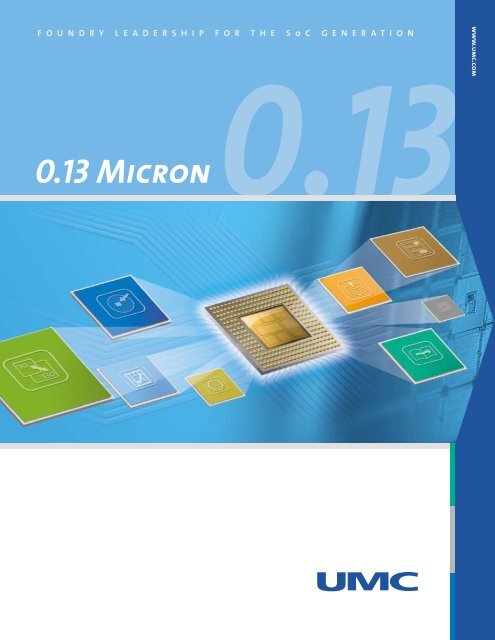
F O U N D R Y L E A D E R S H I P F O R T H E S o C G E N E R A T I O N<br />
<strong>0.13</strong> <strong>Micron</strong><br />
<strong>0.13</strong><br />
www.umc.com
<strong>0.13</strong> <strong>Micron</strong><br />
Key Features<br />
• Integrated flows for Logic,<br />
Mixed-Signal/RF<br />
• 2.28um 2 SRAM bit cell<br />
• e-Fuse option<br />
• Shallow trench isolation<br />
• Retrograde twin well<br />
(Triple well option)<br />
• Dual gate oxides<br />
• CoSi 2<br />
process<br />
• Up to 1P8M Cu with FSG<br />
dielectric<br />
<strong>UMC</strong>'s mainstream <strong>0.13</strong>um technology is in volume production for a wide<br />
range of customer products in the computer, consumer, and communications<br />
sectors. This technology is supported by a complete SoC solution package that<br />
includes IP, library, EDA tool and other resources to help you achieve volume<br />
production of your SoC product in the shortest time possible.<br />
Customers can also take advantage of <strong>UMC</strong>'s world leading manufacturing<br />
capabilities to realize maximum competitive advantages. 300mm production<br />
and industry leading yields and cycle times ensure that you can maximize<br />
your productivity for better cost efficiencies for volume production of your<br />
design.<br />
Furthermore, with <strong>UMC</strong>'s 0.11um process, customers can enjoy lower<br />
production cost while keeping the same performance. This production proven<br />
half node technology increases gross die per wafer.<br />
• BOAC (Bonding Over Active<br />
Circuit)<br />
• Wire Bond / Flip Chip option<br />
<strong>0.13</strong>um SoC Process Platform<br />
<strong>UMC</strong>'s <strong>0.13</strong>-micron SoC solution begins with a<br />
flexible technology design platform. Customers<br />
are able to choose from a variety of process<br />
device options optimized for their specific<br />
application, such as High Speed (HS), Standard<br />
Performance (SP), Low Leakage (LL), or the unique<br />
Fusion process. Other technology options can<br />
then be implemented including mixed signal/<br />
<strong>0.13</strong> <strong>Micron</strong> SoC Technology Platform<br />
Logic Transistor Mixed Signal / RFCMOS Embedded Memories<br />
High Speed (HS)<br />
Low Leakage (LL)<br />
Standard Performance (SP)<br />
Fusion (HS + LL)<br />
Fusion (SP + LL)<br />
Fusion (HS + SP)<br />
Multiple Vt Transistors<br />
3.3V High Gain I/O<br />
Spiral Cu Inductor<br />
MIM Capacitors<br />
Poly/Diffusion Resistors<br />
6T-SRAM: 2.28 um 2 cell size<br />
8T-SRAM: 4.66 um 2 cell size<br />
RFCMOS and embedded memories to further<br />
customize the process.
<strong>0.13</strong>um Device Offerings<br />
<strong>UMC</strong>'s <strong>0.13</strong>um technology features a wide<br />
range of device offerings, each optimized for<br />
different product applications, from high<br />
speed to low leakage. In addition to these core<br />
offerings, RFCMOS/Mixed Signal technologies<br />
are available along with Fusion, a design option<br />
that allows both high speed and low leakage<br />
transistors to be combined on a single chip.<br />
Core Devices<br />
• HS 1.2V<br />
• SP 1.2V<br />
• LL 1.2V<br />
• HS+LL 1.2V<br />
• HS+SP 1.2V<br />
• SP+LL 1.2V<br />
<strong>0.13</strong>um Logic / MS / RF Technology<br />
I/O Devices<br />
MS/RF Devices<br />
• 3.3V I/O<br />
• Resistor<br />
• 3.3V High Gain I/O* • MIM Cap<br />
• Varactor<br />
• Inductor<br />
* For MS/RF only<br />
• Diode<br />
• BJT<br />
• Native Device<br />
Fusion<br />
<strong>UMC</strong>'s innovative Fusion process allows<br />
different transistor devices, such as high<br />
speed and low leakage, to be combined on<br />
the same design. This creates a single chip<br />
solution that offers the advantage of high<br />
performance without sacrificing energy<br />
efficiency, ideal for today's 3G, wireless, and<br />
portable communication products.<br />
HS+LL 1.2V<br />
Fusion Device Offerings<br />
HS+SP 1.2V SP+LL 1.2V<br />
Memory Memory<br />
IP IP Custom Logic<br />
High Speed Logic (HS)<br />
Mixed Block (HS + LL, etc.)<br />
Low Leakage Block (LL)<br />
Memory IP CPU<br />
Fusion SoC Technology<br />
Silicon Verified IP Solutions<br />
<strong>UMC</strong> offers comprehensive design resources<br />
that enable our customers to fully realize the<br />
advantages of <strong>UMC</strong>'s advanced technologies.<br />
<strong>UMC</strong>'s silicon verified fundamental IPs<br />
(standard cells, I/Os, and memory compilers)<br />
help customers easily migrate their designs<br />
to the next process generation to realize<br />
significant performance advantages while also<br />
reducing die size.<br />
Customers can also leverage application<br />
specific IPs that are specialized for all types of<br />
mainstream applications such as digital TVs,<br />
cellular baseband controllers, digital cameras,<br />
and audio players to overcome time-to-market<br />
challenges.<br />
PLL, USB, LVDS,<br />
ADC/DAC,<br />
Embedded<br />
Memory, HDMI,<br />
DDR2<br />
PLL, USB, LVDS,<br />
ADC/DAC,<br />
HDMI, SATA,<br />
Embedded<br />
Memory<br />
DTV<br />
Digital Camera<br />
Mobile DDR, PLL,<br />
ADC/DAC,<br />
LVDS, USB,<br />
Embedded<br />
Memory<br />
PLL, USB, LVDS,<br />
ADC/DAC,<br />
Embedded<br />
Memory<br />
Base Band<br />
Audio Players
Fundamental IP Support for SoC Designs<br />
<strong>UMC</strong> offers comprehensive design resources that support our <strong>0.13</strong>um process technology. Silicon verified fundamental IPs (standard<br />
cells, I/Os, and memory compilers) optimized to <strong>UMC</strong> technologies are available free-of-charge from several leading vendors.<br />
Library Provider<br />
<strong>0.13</strong>um<br />
FARADAY VIRAGE ARM<br />
Library HS SP LL Fusion HS SP LL HS SP LL<br />
Standard Cells Þ Þ Þ Þ Þ Þ<br />
I/O Þ Þ Þ<br />
Single Port SRAM Compiler Þ Þ Þ Þ Þ Þ Þ<br />
Dual Port SRAM Compiler Þ Þ Þ Þ Þ Þ Þ<br />
Single Port Register File Þ Þ Þ Þ Þ Þ<br />
Dual Port Register File Þ Þ Þ Þ Þ Þ Þ<br />
ROM Compiler Þ Þ Þ Þ Þ Þ<br />
Low Power Features of<br />
Standard Cell Library<br />
With today's proliferation of low power applications,<br />
lowering energy consumption without sacrificing<br />
performance has become a critical concern<br />
for designers of power management chips for<br />
portable electronics. <strong>UMC</strong> supports its standard<br />
cell library with low power design features,<br />
including multiple Vt, clock-gating, level shifter<br />
and other features to complement the complete<br />
low power SOC solution.<br />
Operating<br />
Power<br />
Leakage<br />
Power<br />
Type<br />
Voltage Island<br />
& Scaling<br />
Clock Gating<br />
& Frequency<br />
Scaling<br />
Support Features<br />
Level Shifters<br />
w / Insulator<br />
Power &<br />
Timing Model<br />
@ 80% of Vdd<br />
Support<br />
65nm 90nm <strong>0.13</strong>um<br />
Þ Þ Þ<br />
Clock Gated F/F Þ Þ Þ<br />
Multi-Vt Multi-Vt cells Þ Þ Þ<br />
Power Gating<br />
Body Bias<br />
Isolation cells, Retention F/F<br />
Headers / Footers, etc.<br />
Tapless cells<br />
Timing /<br />
Power Model<br />
Þ Þ Þ<br />
Þ Þ Þ<br />
Low Power Design Support<br />
Front-end design<br />
Low leakage<br />
process<br />
Power<br />
gating<br />
Multi Vth<br />
Multi VDD<br />
Low power<br />
synthesis<br />
Clock<br />
gating<br />
Voltage and<br />
frequency scaling<br />
Body bias<br />
Back-end design<br />
80%<br />
60% 40% 20% 20% 40% 60% 80%<br />
Leakage Power Saving<br />
Dynamic Power Saving
<strong>UMC</strong> Reference Design Flow<br />
<strong>UMC</strong> Reference Design Flow provides a design<br />
methodology and f low validated w ith a<br />
“Leon2” system demonstration board. The flow<br />
incorporates 3rd-party EDA vendors’ baseline<br />
design flows to address issues such as timing<br />
closure, signal integrity, leakage power and design<br />
for manufacturability and adopts a hierarchical<br />
design approach built upon silicon validated<br />
process libraries. <strong>UMC</strong> Reference Design Flow<br />
covers from schematic/RTL coding all the way to<br />
GDS-II generation and supports Cadence, Magma,<br />
Mentor and Synopsys EDA tools. All of these tools<br />
have been correlated to <strong>UMC</strong> silicon and can be<br />
interchanged for added flexibility.<br />
I/O & Memory<br />
Simulation View<br />
Timing View<br />
Timing Constraint &<br />
DFT Requirements<br />
Cell Function, Area,<br />
Timing & Power View<br />
Physical & Noise View<br />
DRC/LVS<br />
Rule Deck<br />
Product Definition/Spec & Tech-dependent Setting<br />
RTL Coding & Simulation<br />
Logic Synthesis<br />
Static Timing Analysis & Gate-level Simulation<br />
Floorplan & Partition<br />
Block & Top Implementation<br />
Physical Verification<br />
Tape-out<br />
Reference Design Flow and Vendor Support<br />
<strong>UMC</strong> works with leading EDA tool companies to provide a verified Reference Design Flow program to ensure the accuracy of customer designs<br />
in a proven environment. <strong>UMC</strong> Reference Design Flow program integrates solutions for digital and analog designs and low power solutions<br />
that incorporate the latest DFM resources available from leading third-party providers. Tools can be interchanged for added flexibility.<br />
Features of Design Flow Cadence Synopsys Magma Mentor Ansoft Springsoft<br />
Functional Logic Simulation - - -<br />
Schematic Entry - - - - -<br />
Logic Synthesis - - -<br />
Static Timing Analysis - - -<br />
Timing Closure - - -<br />
Signal Integrity - - -<br />
Floor Planning - - -<br />
Physical Synthesis - - -<br />
Multi-Vt Low Power - - -<br />
Multi-Vdd Low Power - - - - -<br />
Design For Test - - -<br />
Design For Diagnosis - - -<br />
DFM - double via insertion - - -<br />
DFM - dummy metal filling - - -<br />
Circuits Simulation - -<br />
Power Analysis - - -<br />
Layout Editor - - -<br />
Place & Route - - -<br />
Physical Verification - - -<br />
Formal Verification - - - -<br />
Parasitic Extraction - - -<br />
Noise Analysis - - -<br />
RFCMOS/EMDM - - - -<br />
Analog/Mixed Signal - - -<br />
Note: Available
<strong>UMC</strong> e-Fuse Features<br />
<strong>UMC</strong> has developed its own internal e-fuse<br />
solution that offers the benefits of reduced<br />
chip area, better reliability performance, and<br />
shortened repair time compared to using Al<br />
fuses. <strong>UMC</strong> not only delivers the fuse array, but<br />
also the complete functional macro for easy<br />
integration by customers. Customers may also<br />
use e-fuse for the OTP (one time programming)<br />
function to save costs.<br />
Logic Compatible<br />
Complete Functional<br />
IP Macros<br />
Design-Friendly Features<br />
Flexibility<br />
• No extra masks necessary<br />
• Only one extra pad required<br />
• Fuse array, programming circuit, sensing amplifier<br />
• Serial and parallel architecture<br />
• Allows metal routing over fuses (M6 and above)<br />
• Programmable at package level<br />
• Wafer level fuse options<br />
• Package level fuse options<br />
Virtual Inductor Library<br />
<strong>UMC</strong> has worked with its EDA tool partners<br />
to deliver the industry's first parameterized<br />
inductor design kit based on full-wave<br />
simulation: the Virtual Inductor Library (VIL).<br />
The VIL enables RFCMOS designers to create<br />
and simulate custom inductor geometries<br />
that are compatible with <strong>UMC</strong>'s processes.<br />
It is built upon <strong>UMC</strong>'s Electromagnetic<br />
Design Methodology (EMDM), which allows<br />
engineers to easily and accurately create<br />
any RF structure. EMDM gives designers<br />
the flexibility to innovate new geometries<br />
simply by editing parameters such as<br />
diameter, number of turns or width.<br />
Spiral<br />
Differential w/o<br />
center tap<br />
Differential with<br />
center tap<br />
The GUI based VIL can be used to simulate all types of RF inductors.<br />
Stack<br />
Virtual Capacitor Library<br />
<strong>UMC</strong> has worked with its EDA tool partners<br />
to deliver the industry's first parameterized<br />
MOM capacitor design kit based on fullwave<br />
simulation: the Virtual Capacitor Library (VCL).<br />
The VCL enables RFCMOS designers to create<br />
and simulate custom capacitor geometries<br />
that are compatible with <strong>UMC</strong>'s processes. It<br />
is built upon <strong>UMC</strong>'s Electromagnetic Design<br />
Methodology (EMDM), which allows engineers<br />
to easily and accurately create any RF structure.<br />
EMDM gives designers the flexibility to innovate<br />
new geometries simply by editing parameters<br />
such as number of metal and fingers, arrays,<br />
and length of fingers for capacitor.
MS/RF Design Flow and FDK<br />
The FDK (Foundry Design Kit) provides IC<br />
designers with an automatic design<br />
environment. The methodology provides<br />
access to circuit-level design and simulation,<br />
circuit layout, and layout verification with<br />
accurate RF device models. In the front-end,<br />
fundamental components of <strong>UMC</strong>’s MS/RF<br />
process are implemented in common design<br />
environments and simulation tools. The backend<br />
includes parameterized cells (P Cell), which<br />
include a schematic driven layout to provide an<br />
automatic and complete design flow. Callback<br />
functions are also provided in the design flow<br />
to minimize data entry. EDA tools for MS/RF<br />
designs are also supported.<br />
Schematic (Composer)<br />
(Symbols & CDF)<br />
Schematic Driven Layout<br />
Circuit Layout<br />
Virtuoso(P-cell)<br />
Verification&Extraction<br />
(DRC/LVS/LPE)<br />
Calibre/XRC<br />
Assura<br />
Tape Out<br />
Virtual Inductor/<br />
Capacitor/Spec.<br />
Virtual Inductor/<br />
Capacitor/Library<br />
Virtual Inductor<br />
/Capacitor Library<br />
Spectre/Spectre RF<br />
Artist<br />
Spectre/Spectre RF<br />
Spectre/Spectre RF<br />
Simulator with<br />
Verified<br />
RF/Mixed Signal Models<br />
Optimum Inductor Finder (OIF)<br />
<strong>UMC</strong> offers the Optimum Inductor Finder (OIF) in the FDK package. The OIF gives designers the ability to quickly access a large library<br />
of inductors calibrated to <strong>UMC</strong>'s silicon. It also allows users to perform inductor optimization through just a few simple steps with the<br />
user-friendly interface. For instance, customers can define a desired inductance and make trade-offs between Q-factor and area. The<br />
OIF will select from its inductor library a design that best fits the specifications in a matter of seconds.<br />
Optimum Capacitor Finder (OCF)<br />
<strong>UMC</strong> offers the Optimum Capacitor Finder (OCF) in the FDK package. The OCF gives designers the ability to quickly access a large library<br />
of capacitors calibrated to <strong>UMC</strong>'s silicon. It also allows users to perform capacitor optimization through just a few simple steps with<br />
the user-friendly interface. For instance, customers can define a desired capacitor and make trade-offs between Q-factor and area. The<br />
OCF will select from its capacitor library a design that best fits the specifications in a matter of seconds.<br />
Analog Design Methodology<br />
FDK EDA Supported Tools<br />
MS/RF<br />
Design Flow<br />
Cadence Mentor ADS Synopsys<br />
Schematic Entry<br />
Composer<br />
ADS<br />
Pre-simulation<br />
Hspice/Spectre<br />
Models<br />
Spectre<br />
SpectreRF<br />
Eldo<br />
EldoRF<br />
ADS<br />
HSPICE<br />
Physical Design<br />
Virtuoso XL<br />
Physical<br />
Verification<br />
(DRC/LVS/RCX)<br />
Assura<br />
Assura RCX<br />
Calibre<br />
Calibre XRC<br />
Hercules<br />
Star RCXT
www.umc.com<br />
F O U N D R Y L E A D E R S H I P F O R T H E S o C G E N E R A T I O N<br />
To take advantage of today’s most<br />
comprehensive SoC foundry solutions,<br />
please contact one of our worldwide<br />
sales offices.<br />
North America:<br />
<strong>UMC</strong> USA<br />
488 De Guigne Drive,<br />
Sunnyvale, CA 94085, USA<br />
Tel: 1-408-523-7800<br />
Fax: 1-408-733-8090<br />
Email: sales@umc-usa.com<br />
Asia:<br />
<strong>UMC</strong><br />
No. 3, Li-Hsin 2nd Road,<br />
Hsinchu Science Park,<br />
Hsinchu, Taiwan, R.O.C.<br />
Tel: 886-3-578-2258<br />
Fax: 886-3-577-9392<br />
Email: sales@umc.com<br />
Europe:<br />
<strong>UMC</strong> Europe BV<br />
De entree 77<br />
1101 BH Amsterdam Zuidoost<br />
The Netherlands<br />
Tel: 31-(0)20-5640950<br />
Fax: 31-(0)20-6977826<br />
Email:europe@umc.com<br />
Japan:<br />
<strong>UMC</strong> Japan<br />
15F Akihabara Centerplace Bldg.,<br />
1 Kanda Aioi-Cho Chiyoda-Ku<br />
Tokyo 101-0029 Japan<br />
Tel : +81-3-5294-2701<br />
Fax: +81-3-5294-2707<br />
Email: foundry@umcj.com<br />
Singapore:<br />
<strong>UMC</strong>-SG<br />
No. 3, Pasir Ris Drive 12,<br />
Singapore 519528<br />
Tel: +65-6213-0018<br />
Fax: +65-6213-0008<br />
For more information: visit www.umc.com or e-mail sales@umc.com<br />
0411