Qualcomm's Assessment of 3D Interconnect Equipment ... - Sematech
Qualcomm's Assessment of 3D Interconnect Equipment ... - Sematech
Qualcomm's Assessment of 3D Interconnect Equipment ... - Sematech

Create successful ePaper yourself
Turn your PDF publications into a flip-book with our unique Google optimized e-Paper software.
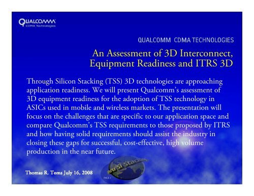
An <strong>Assessment</strong> <strong>of</strong> <strong>3D</strong> <strong>Interconnect</strong>,<br />
<strong>Equipment</strong> Readiness and ITRS <strong>3D</strong><br />
Through Silicon Stacking (TSS) <strong>3D</strong> technologies are approaching<br />
application readiness. We will present Qualcomm’s assessment <strong>of</strong><br />
<strong>3D</strong> equipment readiness for the adoption <strong>of</strong> TSS technology in<br />
ASICs used in mobile and wireless markets. The presentation will<br />
focus on the challenges that are specific to our application space and<br />
compare Qualcomm’s TSS requirements to those proposed by ITRS<br />
and how having solid requirements should assist the industry in<br />
closing these gaps for successful, cost-effective, high volume<br />
production in the near future.<br />
Thomas R. Toms July 16, 2008<br />
PAGE 1
<strong>3D</strong> TSS<br />
• Many Advantages<br />
• Many Challenges<br />
Aggressive Roadmap<br />
Process<br />
Materials<br />
Perception<br />
Technology is<br />
MANY years from<br />
High Volume Production<br />
<strong>Equipment</strong><br />
Design Tools and Methodologies<br />
Cost<br />
<br />
<br />
An Alignment <strong>of</strong> these Challenges with real Applications<br />
<strong>3D</strong> TSS Technology can be implemented sooner<br />
Thomas R Toms July 16, 2008<br />
PAGE 2
Outline<br />
• Terminology<br />
• Growth in mobile and wireless markets<br />
• Capabilities vs. Application driven <strong>3D</strong><br />
• A TSS case study<br />
TSV selection counts/tier<br />
Si Growth<br />
Tier to Tier interconnects<br />
Si tier thickness<br />
Feature size vs. Throughput and Yield<br />
• Issues for TSS<br />
• Concluding remarks<br />
Thomas R Toms July 16, 2008<br />
PAGE 3
Terminology<br />
3 Tier TSS<br />
TSS – Through Silicon Stacking<br />
AF – The active face <strong>of</strong> the silicon wafer/die<br />
BF – The back face side <strong>of</strong> the wafer/die<br />
TSV – Through Silicon Via<br />
KOA – Keep Out Area<br />
Tier – 2D Silicon layer<br />
T2T – Tier to Tier<br />
RDLB – A BF metal layer<br />
Tier 2<br />
Tier 1<br />
BF<br />
Tier 3<br />
T2T<br />
RDLB<br />
KOA<br />
Farm – An N by M array <strong>of</strong> TSVs connected to the same circuit node<br />
TSV<br />
Farm<br />
AF<br />
Thomas R Toms July 16, 2008<br />
PAGE 4
Growth in mobile and wireless markets<br />
In 2007 Qualcomm shipped<br />
273 million MSM chips,<br />
up 25% from 2006. For<br />
the latest quarter<br />
Qualcomm shipped ~85<br />
million MSM chips, up<br />
39% year-over-year<br />
2<br />
1<br />
Global Handset Demand in Billions<br />
Source: ABI Research<br />
Smartphone/Feature Phone<br />
Enhanced Phone<br />
Low-End<br />
Source: Qualcomm Q2 FY08 Earnings<br />
April 23, 2008, Pages 4, 13<br />
0<br />
2006 2007 2008 2009 2010 2011 2012<br />
Thomas R Toms July 16, 2008<br />
PAGE 5
Which comes first<br />
Capabilities driven vs. Application driven requirements<br />
The equipment or the design<br />
High density TSV and T2T or the µ-architecture to use the very large bandwidth that<br />
TSS <strong>of</strong>fers<br />
Cost-effective, high volume TSS production for mobile and wireless or High<br />
performance TSS applications<br />
volume ramp<br />
qualification<br />
development<br />
study<br />
time<br />
Thomas R Toms July 16, 2008<br />
PAGE 6
ITRS Draft Specification for <strong>3D</strong><br />
30K<br />
TSV/mm 2 vs. Year at 1% TSV KOA<br />
Source:<br />
INTERNATIONAL TECHNOLOGY ROADMAP<br />
FOR SEMICONDUCTORS<br />
2007 EDITION<br />
INTERCONNECT page 46<br />
TSV count<br />
25K<br />
20K<br />
15K<br />
10K<br />
5K<br />
Year:<br />
1315 – 3248 TSV/mm 2<br />
Small TSV<br />
Large TSV<br />
2007 2008 2009 2010 2011 2012 2013 2014 2015<br />
Acceptable TSV Densities<br />
Thomas R Toms July 16, 2008<br />
PAGE 7<br />
backup
A TSS case study<br />
What impact does the TSV type, TSV pitch, # <strong>of</strong> tiers, TSV farm size, TSV<br />
size, bonding order, Metallization layers and T2T bonding pitch have on<br />
the COO and Yield<br />
Factors<br />
TSV 1 st or Last<br />
Power delivery (PDN)<br />
A single supply, Number <strong>of</strong> TSS tiers, intra-tier I*R losses and TSV I*R losses<br />
External I/O count and Si tier size<br />
For this study the I/O count was fixed at 400<br />
The number <strong>of</strong> T2T signals (non-power/ground)<br />
Via last - 200 (the approximate I/O count for two 64 bit channels <strong>of</strong> DDR1 memory)<br />
Via 1 st - 2500 (arbitrarily selected)<br />
The Si tier size<br />
Base tier size <strong>of</strong> 50 – 100mm 2<br />
Thomas R Toms July 16, 2008<br />
PAGE 8
TSV selection<br />
TSV Keep Out Area (KOA) and availability<br />
Via Last<br />
Via 1 st<br />
6000<br />
150<br />
KOA (<br />
(µm 2 /TSV)<br />
5000<br />
4000<br />
3000<br />
2000<br />
1000<br />
125<br />
100<br />
75<br />
50<br />
25<br />
0<br />
Today 2009 2010<br />
0<br />
Today 2010<br />
200mm Wafers<br />
300mm Wafers<br />
200mm Wafers 300mm Wafers (50um) 300mm Wafers (25um)<br />
Thomas R Toms July 16, 2008<br />
PAGE 9
Tier Growth<br />
12%<br />
Tier Growth<br />
9%<br />
6%<br />
3%<br />
0%<br />
AF2AF no RDL AF2BF no RDL AF2AF with RDL AF2BF with RDL<br />
Via 1 st is the reasonable selection for the<br />
TSV based on the area impact<br />
Via Last Via 1st<br />
RDL reduces PDN lateral resistance by 90%<br />
Via Last 2010 300mm Wafer<br />
400 I/O (TSV farm 1x1)<br />
200 T2T (TSV farm 1x1)<br />
Via 1 st 2010 300mm Wafer (50µm)<br />
400 I/O (TSV farm 2x2)<br />
2500 T2T (TSV farm 1x1)<br />
Thomas R Toms July 16, 2008<br />
PAGE 10
Power & Ground in a TSS stack<br />
How many TSV and T2T connections are required to distribute<br />
power and ground<br />
PDN TSV Requirements<br />
TSV I*R pitch<br />
TSV farm pitch<br />
200 µm<br />
Intra-Tier I*R pitch<br />
TSV farm density<br />
50/mm 2<br />
TSV farm density<br />
Low Tier Count High<br />
Thomas R Toms July 16, 2008<br />
PAGE 11
Tier to Tier connection pitch<br />
T2T Pitch(µm)<br />
40<br />
30<br />
20<br />
T2T Pitch<br />
ITRS Draft Specification for <strong>3D</strong> (larger pitch)<br />
Pitch for 1:1 match <strong>of</strong> large TSV KOA count (page 7)<br />
Current T2T<br />
Application<br />
needs<br />
Future<br />
needs<br />
10<br />
Year:<br />
2007 2008 2009 2010 2011 2012 2013 2014 2015<br />
Thomas R Toms July 16, 2008<br />
PAGE 12<br />
backup
Factors that impact Tier thickness<br />
• TSV 1 st with a constant aspect ratio<br />
Resistance<br />
Capacitance/KOA<br />
Cost<br />
Yield<br />
• Thin tier handling<br />
Cost<br />
Yield<br />
?<br />
?<br />
?<br />
? ? ?<br />
?<br />
?<br />
25µm?<br />
There are various “?” that must be determined before the<br />
optimum tier thickness can be selected<br />
To be conservative Qualcomm is targeting thicker (50 µm<br />
minimum) vs. the thinner tier that shall be available for<br />
TSS products<br />
50µm?<br />
Thickness<br />
Thomas R Toms July 16, 2008<br />
PAGE 13
TSS cost models<br />
Qualcomm has access to several TSS cost models but all lack two key inputs<br />
COO – What are the equipment throughputs and consumables vs. TSS feature<br />
specifications and time<br />
Yield – The yield function <strong>of</strong> TSS processes and time<br />
What is the TSS system COO in 2 – 3 or more years<br />
Process COO<br />
Acceptable COO<br />
Time<br />
TSS Process Options<br />
A B C D<br />
Time<br />
Process Yield<br />
100%<br />
98%<br />
96%<br />
94%<br />
92%<br />
90%<br />
Thomas R Toms July 16, 2008<br />
PAGE 14
Feature size vs. Throughput and Yield<br />
• COO & Yields for TSS<br />
Function <strong>of</strong> feature size<br />
Standardization<br />
• Qualcomm has defined TSS feature size to standardize, improve throughput<br />
and yields; while, meeting our anticipated µ-architecture needs<br />
• Qualcomm TSS feature size requirements are relaxed compared to the data in<br />
the 2007 ITRS <strong>3D</strong> targets by<br />
Tier Thickness 2 – 10X<br />
TSV pitch/size 4 – 9X<br />
T2T pitch 7 – 10X<br />
Thomas R Toms July 16, 2008<br />
PAGE 15
Issues revealed by the TSS case study<br />
• ITRS <strong>3D</strong> feature projections are too aggressive for the needs <strong>of</strong> an early adoption <strong>of</strong> TSS<br />
in mobile and wireless markets<br />
Are these aggressive requirements driving higher COO?<br />
Are the requirements based on niche or mainstream applications needs?<br />
• Key Questions to be answered in relaxing the TSS requirements<br />
Will more relaxed targets reduce the COO?<br />
Improve yields to an acceptable level for HVM?<br />
Will relaxed requirements accelerate the adoption <strong>of</strong> TSS?<br />
• <strong>Equipment</strong>, materials and processes gaps that need to be closed for successful, costeffective,<br />
high volume production<br />
Predictive COO and Yield information for use in the TSS cost models – process<br />
HVM 300mm Die to Wafer alignment – equipment<br />
Low temperature Tier to Tier bonding – material and equipment<br />
Backside metallization on thinned TSS Si wafer – process and equipment<br />
More in backup<br />
Thomas R Toms July 16, 2008<br />
PAGE 16
Concluding remarks<br />
To improve the situation Qualcomm has defined a set <strong>of</strong> requirements for TSS<br />
with our Foundry and SAT partners. These define both short term and longer<br />
term targets for adoption <strong>of</strong> TSS technology in the mobile and wireless markets.<br />
It is our belief that having defined requirements for TSS will assist the industry<br />
in closing the gaps for successful, cost-effective, high volume production in the<br />
near future.<br />
Thomas R Toms July 16, 2008<br />
PAGE 17
Contributors<br />
I would like to than the following people at Qualcomm who helped put this<br />
presentation together<br />
Arvind Chandrasekaran<br />
Sam Gu<br />
Rakesh Kumar<br />
Matt Nowak<br />
Riko Radojcic<br />
Urmi Ray<br />
Thomas R Toms July 16, 2008<br />
PAGE 18
Thank You<br />
PAGE 19
Backup material<br />
Thomas R Toms July 16, 2008<br />
PAGE 20
Calculation <strong>of</strong> TSV count for 1% tier growth<br />
KOA assumptions<br />
TSV KOA = 2X TSV area<br />
TSV KOA shape is circular<br />
Ignores standard cell step size<br />
TSV KOA = 0.5 * pi * (TSV diameter) 2<br />
1% <strong>of</strong> 1mm 2 = 10,000µm 2<br />
TSV count = 10,000/TSV KOA<br />
For example using the 2008 ITRS TSV diameters:<br />
TSV diameter: 1.4 – 2.2µm<br />
Small TSV KOA = 0.5 * pi * (1.4µm) 2 = 3.078µm 2<br />
Small TSV count = 10000/3.078 = 3248<br />
Large TSV KOA = 0.5 * pi * (2.2µm) 2 = 7.603µm 2<br />
Large TSV count = 10000/7.603 = 1315<br />
Thomas R Toms July 16, 2008<br />
PAGE 21<br />
Return
Calculation <strong>of</strong> Tier to Tier connection pitch<br />
The number <strong>of</strong> T2T bonds that are required for the PDN is equivalent to the number<br />
<strong>of</strong> TSV farms (~50/mm 2 )<br />
A reasonable tier size for the 2500 T2T I/O signals <strong>of</strong> 50 – 100mm 2<br />
Average T2T I/O density would be 25 – 50/mm 2<br />
Sum the PDN and I/O to get an average T2T connection density <strong>of</strong> 75 – 100/mm 2<br />
To provide floor planning flexibility and to minimize routing distances increase the<br />
T2T density by 8-12<br />
Resulting T2T pitch 28.8 – 40.8µm<br />
In the future (3 – 6 years) it is anticipated that<br />
2D Si process continues to scale<br />
The µ-architecture changes to take greater advantage <strong>of</strong> TSS<br />
Results in the T2T densities and I/O counts increase<br />
Anticipate a heterogeneous TSS stack shall require another 4-8 fold increase in the T2T<br />
density<br />
Resulting T2T pitch 10.1 – 20.4µm<br />
Thomas R Toms July 16, 2008<br />
PAGE 22<br />
Return
300mm <strong>Equipment</strong>/Process/Materials Gaps Table<br />
High – Level Module<br />
<strong>Equipment</strong><br />
Process<br />
Material<br />
Wafer crack during demount<br />
Adhesive max temperature<br />
Carrier (Mount/Demount)<br />
Lead time, cost<br />
µbump<br />
conformality<br />
Carrier material selection<br />
Number <strong>of</strong> carrier cycles<br />
Adhesive residue<br />
TSV Contact preparation<br />
CMP<br />
PECVD<br />
TTV process optimization<br />
Passivation material<br />
(stress/temperature)<br />
RDL<br />
BF Alignment<br />
Stepper resolution<br />
Planarity<br />
Polymer temperature<br />
T2T Bonding<br />
Bonding accuracy<br />
Under fill<br />
Material stack up<br />
TSS stack assembly<br />
TSS stack bumping<br />
Thomas R Toms July 16, 2008<br />
PAGE 23<br />
Return