Low Bias Electron Scattering in Structure ... - Researcher - IBM
Low Bias Electron Scattering in Structure ... - Researcher - IBM
Low Bias Electron Scattering in Structure ... - Researcher - IBM

Create successful ePaper yourself
Turn your PDF publications into a flip-book with our unique Google optimized e-Paper software.
PRL 107, 146601 (2011) PHYSICAL REVIEW LETTERS<br />
week end<strong>in</strong>g<br />
30 SEPTEMBER 2011<br />
In order to exam<strong>in</strong>e whether the observed superl<strong>in</strong>ear<br />
temperature dependence of could arise from SWNT<br />
optical phonon modes [20], a numerical model is developed<br />
that calculates T ð Þ by solv<strong>in</strong>g the Boltzmann transport<br />
equation us<strong>in</strong>g a s<strong>in</strong>gle electron-phonon coupl<strong>in</strong>g<br />
g ¼ 5:3 eV= A [9]. This value of g provides the strength<br />
of the scatter<strong>in</strong>g matrix element with all the vibrational<br />
modes <strong>in</strong> the carbon nanotube (CNT) structure described<br />
by the phonon model [21]. The small-dashed l<strong>in</strong>e <strong>in</strong> Fig. 3<br />
represents the results from this model for the measured<br />
ð26; 11Þ SWNT. This model does <strong>in</strong>deed cause nonl<strong>in</strong>earity<br />
<strong>in</strong> T ð Þ. However, the calculated magnitude of the additional<br />
scatter<strong>in</strong>g is not sufficient to expla<strong>in</strong> the experiments.<br />
More fundamentally, the onset of optical phonon<br />
scatter<strong>in</strong>g ( 300 K) reflects the frequency of the radial<br />
breath<strong>in</strong>g mode, which has a well-established dependence<br />
on nanotube structure. Therefore, use of a structurally<br />
def<strong>in</strong>ed nanotube allows us to def<strong>in</strong>itively rule out radial<br />
breath<strong>in</strong>g mode scatter<strong>in</strong>g as the source of the observed<br />
superl<strong>in</strong>ear T ð Þ behavior from 100 to 300 K.<br />
Rul<strong>in</strong>g out contributions from acoustic and optical nanotube<br />
phonons as well as adsorbate-<strong>in</strong>duced scatter<strong>in</strong>g<br />
leaves only phonon modes of the underly<strong>in</strong>g substrates as<br />
a probable cause for the low electronic mean free path<br />
observed <strong>in</strong> the experiments. Similar substrate phonons<br />
have been shown to play a large role <strong>in</strong> transport properties<br />
of graphene [22], and a theoretical study on semiconduct<strong>in</strong>g<br />
SWNTs predicted the SPP modes to be important [23].<br />
To <strong>in</strong>vestigate the role of SPP scatter<strong>in</strong>g on metallic SWNT<br />
transport, its effect is <strong>in</strong>cluded <strong>in</strong> the resistivity calculations<br />
for the ð26; 11Þ SWNT. The strength of the SPP<br />
phonon scatter<strong>in</strong>g depends on the distance from the CNT<br />
to the polar substrate h and the dielectric properties of the<br />
substrate [24]. The coupl<strong>in</strong>g is strongest when the azimuthal<br />
angular momentum is conserved [25], for which case<br />
the scatter<strong>in</strong>g rate of an electron with momentum k has the<br />
form [23]<br />
1<br />
k<br />
¼ 2 @<br />
Z<br />
dq<br />
e 2 @! so<br />
<br />
e 2hq<br />
<br />
1<br />
1 þ 1<br />
<br />
1<br />
0 þ 1<br />
p<br />
qd ffiffiffiffiffiffiffiffiffiffiffiffiffiffiffiffiffiffiffiffiffiffiffiffiffiffiffi ½n so ð" k " kþq þ @! so Þ<br />
2qðd þ 2hÞ<br />
þð1 þ n so Þð" k " kþq @! so ÞŠ; (1)<br />
where 0 and 1 are the low- and high-frequency dielectric<br />
constants of the polar substrate, respectively, d is the<br />
tube diameter, @! so is the SPP energy, and n so is the Bose-<br />
E<strong>in</strong>ste<strong>in</strong> occupation number, which leads to the activated<br />
temperature dependence. These material properties can be<br />
measured <strong>in</strong>dependently, and we use their values for<br />
SiO 2 [25] and AlN [26]. The distance from the CNT to<br />
the substrate is fixed at the van der Waals distance of<br />
h ¼ 3:5 A. The temperature dependence shown <strong>in</strong> Fig. 3<br />
is measured when the device is <strong>in</strong> the on state, i.e.,<br />
V g -V n ¼ 8V, where V n is a gate voltage correspond<strong>in</strong>g<br />
to the CNT <strong>in</strong> the charge neutral state. Us<strong>in</strong>g a<br />
classical electrostatic capacitance C g ¼ 2"" 0 =lnð4t=dÞ<br />
0:34 pF=cm for the CNT on t ¼ 300 nm SiO 2 with " ¼ 3:9,<br />
we can estimate a charge carrier density of n 1:7e=nm.<br />
For such a charge carrier density, the Fermi level is expected<br />
to lie with<strong>in</strong> the first metallic band <strong>in</strong> a 2 nm<br />
diameter CNT. Figure 3 shows the simulated temperaturedependent<br />
resistivity <strong>in</strong>clud<strong>in</strong>g SPP scatter<strong>in</strong>g for this<br />
dop<strong>in</strong>g level (solid l<strong>in</strong>e). The SPP model accurately predicts<br />
the superl<strong>in</strong>ear trend as well as absolute resistivity<br />
values. The robustness of the fit, particularly its dependence<br />
on the distance to the substrate h, is discussed <strong>in</strong><br />
detail <strong>in</strong> Ref. [27]. When h is changed by 30%, there is a<br />
15%–20% change observed <strong>in</strong> (400 K). Most importantly,<br />
because the onset temperature of SPP scatter<strong>in</strong>g<br />
depends only on the known SPP energy, the close agreement<br />
between the theory and experiment for the onset of<br />
superl<strong>in</strong>ear behavior <strong>in</strong> T ð Þ at 100 K provides direct<br />
evidence for the SPP scatter<strong>in</strong>g mechanism that does not<br />
depend on any adjustable parameters.<br />
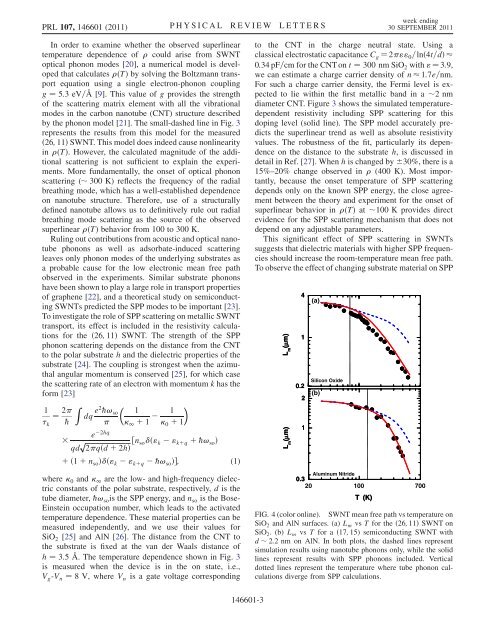
This significant effect of SPP scatter<strong>in</strong>g <strong>in</strong> SWNTs<br />
suggests that dielectric materials with higher SPP frequencies<br />
should <strong>in</strong>crease the room-temperature mean free path.<br />
To observe the effect of chang<strong>in</strong>g substrate material on SPP<br />
L m (µm)<br />
L m (µm)<br />
4<br />
1<br />
0.2<br />
2<br />
1<br />
(a)<br />
Silicon Oxide<br />
(b)<br />
Alum<strong>in</strong>um Nitride<br />
0.3<br />
20 100 700<br />
T (K)<br />
FIG. 4 (color onl<strong>in</strong>e). SWNT mean free path vs temperature on<br />
SiO 2 and AlN surfaces. (a) L m vs T for the ð26; 11Þ SWNT on<br />
SiO 2 . (b) L m vs T for a ð17; 15) semiconduct<strong>in</strong>g SWNT with<br />
d 2:2 nmon AlN. In both plots, the dashed l<strong>in</strong>es represent<br />
simulation results us<strong>in</strong>g nanotube phonons only, while the solid<br />
l<strong>in</strong>es represent results with SPP phonons <strong>in</strong>cluded. Vertical<br />
dotted l<strong>in</strong>es represent the temperature where tube phonon calculations<br />
diverge from SPP calculations.<br />
146601-3