PRL 107, 146601 (2011) PHYSICAL REVIEW LETTERS week end<strong>in</strong>g 30 SEPTEMBER 2011 scatter<strong>in</strong>g, a 2 nm diameter semiconduct<strong>in</strong>g SWNT (with undeterm<strong>in</strong>ed chirality) is transfer-pr<strong>in</strong>ted on an AlN layer deposited over degenerately doped silicon. Figure 4 compares the temperature dependence of L m for the previously described ð26; 11Þ SWNT on SiO 2 and the semiconduct<strong>in</strong>g SWNT on AlN. The fitted l<strong>in</strong>es represent the numerical model results with and without the <strong>in</strong>clusion of SPP scatter<strong>in</strong>g from respective substrates. The numerical model accurately predicts the experiments on the AlN surface (at n ¼ 1:1e=nm). The vertical dotted l<strong>in</strong>es po<strong>in</strong>t to the onset temperature of the SPP scatter<strong>in</strong>g modes. It is clear from Fig. 4 that AlN surface phonon modes start contribut<strong>in</strong>g to carrier scatter<strong>in</strong>g at a much higher temperature than on SiO 2 . This provides further confirmation of the SPP scatter<strong>in</strong>g model and also <strong>in</strong>dicates that substrate materials with higher SPP energies such as AlN should <strong>in</strong>crease the performance of nanotube-based devices near room temperature. We note that, although it would have been preferable to use known-chirality nanotubes for both tests, the model shows weak dependence of SPP scatter<strong>in</strong>g on chirality [27]. In summary, we have measured the temperaturedependent resistivity of a known-chirality metallic SWNT over a wide temperature range, <strong>in</strong> UHV. Our measurements elim<strong>in</strong>ate adsorbates, acoustic phonons, and optical phonons as the cause for the anomalously low L m measured for SWNTs and identify the SPP modes as the dom<strong>in</strong>ant scatterers. The experiments on SWNTs deposited over an AlN surface are consistent with this conclusion. The accompany<strong>in</strong>g theoretical analysis that <strong>in</strong>cludes the <strong>in</strong>tr<strong>in</strong>sic and SPP phonon modes reproduces the experiments very well. These results po<strong>in</strong>t towards the importance of substrate selection <strong>in</strong> maximiz<strong>in</strong>g the electronic mean free path <strong>in</strong> SWNTs. We acknowledge support from the National Science Foundation under collaborative Grants No. DMR- 1006230 (M. I.) and No. DMR-1006533 (J. H.), the U.S. Department of Energy under Grant No. DE-FG02- 07ER15842 (T. F. H.), Honda Motor Company, and Intel Company. B. C. was funded by an Intel PhD Fellowship. *To whom all correspondence should be addressed. bchandr@us.ibm.com [1] S. List et al., Microelectron. Eng. 83, 2200 (2006). [2] R. H. Baughman, A. A. Zakhidov, and W. A. de Heer, Science 297, 787 (2002). [3] A. Javey et al., Phys. Rev. Lett. 92, 106804 (2004). [4] M. S. Purewal et al., Phys. Rev. Lett. 98, 186808 (2007). [5] J. Y. Park et al., Nano Lett. 4, 517 (2004). [6] D. Mann et al., Nano Lett. 3, 1541 (2003). [7] P. Sundqvist et al., Nano Lett. 7, 2568 (2007). [8] C. L. Kane et al., Europhys. Lett. 41, 683 (1998). [9] V. Perebe<strong>in</strong>os, J. Tersoff, and P. Avouris, Phys. Rev. Lett. 94, 086802 (2005). [10] G. Penn<strong>in</strong>gton and N. Goldsman, Phys. Rev. B 68, 045426 (2003). [11] Z. Yao, C. L. Kane, and C. Dekker, Phys. Rev. Lett. 84, 2941 (2000). [12] L. M. Huang et al., J. Phys. Chem. B 108, 16 451 (2004). [13] B. Chandra et al., Phys. Status Solidi B 243, 3359 (2006). [14] M. Y. Sfeir et al., Science 312, 554 (2006). [15] M. Y. Sfeir et al., Science 306, 1540 (2004). [16] X. M. H. Huang et al., Nano Lett. 5, 1515 (2005). [17] M. Ouyang et al., Science 292, 702 (2001). [18] V. V. Deshpande et al., Science 323, 106 (2009). [19] S. He<strong>in</strong>ze et al., Phys. Rev. Lett. 89, 106801 (2002). [20] E. Pop et al., J. Appl. Phys. 101, 093710 (2007). [21] V. Perebe<strong>in</strong>os and J. Tersoff, Phys. Rev. B 79, 241409 (2009). [22] J. H. Chen et al., Nature Nanotech. 3, 206 (2008). [23] V. Perebe<strong>in</strong>os et al., Nano Lett. 9, 312 (2009). [24] S. Q. Wang and G. D. Mahan, Phys. Rev. B 6, 4517 (1972). [25] A. G. Petrov and S. V. Rotk<strong>in</strong>, JETP Lett. 84, 156 (2006). [26] M. V. Fischetti, D. A. Neumayer, and E. A. Cartier, J. Appl. Phys. 90, 4587 (2001). [27] See Supplemental Material at http://l<strong>in</strong>k.aps.org/ supplemental/10.1103/PhysRevLett.107.146601 for dependence of the CNT mean free path on the surface to CNT distance and CNT chirality. 146601-4
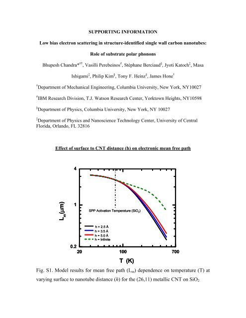
SUPPORTING INFORMATION <strong>Low</strong> bias electron scatter<strong>in</strong>g <strong>in</strong> structure-identified s<strong>in</strong>gle wall carbon nanotubes: Role of substrate polar phonons Bhupesh Chandra* #† , Vasilli Perebe<strong>in</strong>os # , Stéphane Berciaud § , Jyoti Katoch ‡ , Masa Ishigami ‡ , Philip Kim § , Tony F. He<strong>in</strong>z § , James Hone † † Department of Mechanical Eng<strong>in</strong>eer<strong>in</strong>g, Columbia University, New York, NY10027 # <strong>IBM</strong> Research Division, T.J. Watson Research Center, Yorktown Heights, NY10598 § Department of Physics, Columbia University, New York, NY 10027 ‡ Department of Physics and Nanoscience Technology Center, University of Central Florida, Orlando, FL 32816 Effect of surface to CNT distance (h) on electronic mean free path 4 L m (μm) 1 SPP Activation Temperature (SiO 2 ) h = 2.5 Å h = 3.5 Å h = 5.0 Å h = Inf<strong>in</strong>ite 0.2 20 100 700 T (K) Fig. S1. Model results for mean free path (L m ) dependence on temperature (T) at vary<strong>in</strong>g surface to nanotube distance (h) for the (26,11) metallic CNT on SiO 2