WM8758B, Rev 4.4 - Wolfson Microelectronics plc
WM8758B, Rev 4.4 - Wolfson Microelectronics plc
WM8758B, Rev 4.4 - Wolfson Microelectronics plc

Create successful ePaper yourself
Turn your PDF publications into a flip-book with our unique Google optimized e-Paper software.
w<br />
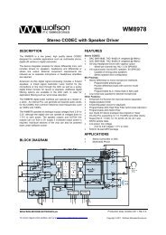
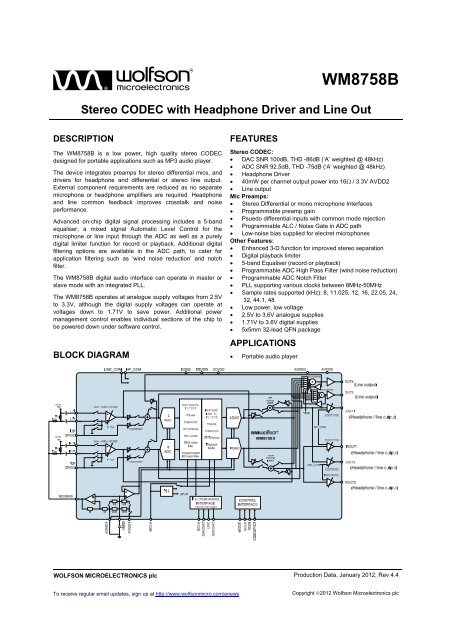
<strong>WM8758B</strong><br />
Stereo CODEC with Headphone Driver and Line Out<br />
DESCRIPTION<br />
The <strong>WM8758B</strong> is a low power, high quality stereo CODEC<br />
designed for portable applications such as MP3 audio player.<br />
The device integrates preamps for stereo differential mics, and<br />
drivers for headphone and differential or stereo line output.<br />
External component requirements are reduced as no separate<br />
microphone or headphone amplifiers are required. Headphone<br />
and line common feedback improves crosstalk and noise<br />
performance.<br />
Advanced on-chip digital signal processing includes a 5-band<br />
equaliser, a mixed signal Automatic Level Control for the<br />
microphone or line input through the ADC as well as a purely<br />
digital limiter function for record or playback. Additional digital<br />
filtering options are available in the ADC path, to cater for<br />
application filtering such as ‘wind noise reduction’ and notch<br />
filter.<br />
The <strong>WM8758B</strong> digital audio interface can operate in master or<br />
slave mode with an integrated PLL.<br />
The <strong>WM8758B</strong> operates at analogue supply voltages from 2.5V<br />
to 3.3V, although the digital supply voltages can operate at<br />
voltages down to 1.71V to save power. Additional power<br />
management control enables individual sections of the chip to<br />
be powered down under software control.<br />
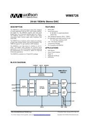
BLOCK DIAGRAM<br />
FEATURES<br />
Stereo CODEC:<br />
DAC SNR 100dB, THD -86dB (‘A’ weighted @ 48kHz)<br />
ADC SNR 92.5dB, THD -75dB (‘A’ weighted @ 48kHz)<br />
Headphone Driver<br />
40mW per channel output power into 16 / 3.3V AVDD2<br />
Line output<br />
Mic Preamps:<br />
Stereo Differential or mono microphone Interfaces<br />
Programmable preamp gain<br />
Psuedo differential inputs with common mode rejection<br />
Programmable ALC / Noise Gate in ADC path<br />
Low-noise bias supplied for electret microphones<br />
Other Features:<br />
Enhanced 3-D function for improved stereo separation<br />
Digital playback limiter<br />
5-band Equaliser (record or playback)<br />
Programmable ADC High Pass Filter (wind noise reduction)<br />
Programmable ADC Notch Filter<br />
PLL supporting various clocks between 8MHz-50MHz<br />
Sample rates supported (kHz): 8, 11.025, 12, 16, 22.05, 24,<br />
32, 44.1, 48<br />
Low power, low voltage<br />
2.5V to 3.6V analogue supplies<br />
1.71V to 3.6V digital supplies<br />
5x5mm 32-lead QFN package<br />
APPLICATIONS<br />
Portable audio player<br />
WOLFSON MICROELECTRONICS <strong>plc</strong><br />
Production Data, January 2012, <strong>Rev</strong> <strong>4.4</strong><br />
To receive regular email updates, sign up at http://www.wolfsonmicro.com/enews<br />
Copyright 2012 <strong>Wolfson</strong> <strong>Microelectronics</strong> <strong>plc</strong>
<strong>WM8758B</strong><br />
Production Data<br />
TABLE OF CONTENTS<br />
DESCRIPTION ....................................................................................................... 1<br />
BLOCK DIAGRAM ................................................................................................ 1<br />
FEATURES ............................................................................................................ 1<br />
APPLICATIONS ..................................................................................................... 1<br />
TABLE OF CONTENTS ......................................................................................... 2<br />
PIN CONFIGURATION .......................................................................................... 4<br />
ORDERING INFORMATION .................................................................................. 4<br />
PIN DESCRIPTION ................................................................................................ 5<br />
RECOMMENDED OPERATING CONDITIONS ..................................................... 6<br />
ELECTRICAL CHARACTERISTICS ..................................................................... 7<br />
TERMINOLOGY ............................................................................................................ 12<br />
HEADPHONE OUTPUT PERFORMANCE .......................................................... 13<br />
POWER CONSUMPTION .................................................................................... 14<br />
AUDIO PATHS OVERVIEW ................................................................................ 15<br />
SIGNAL TIMING REQUIREMENTS .................................................................... 16<br />
SYSTEM CLOCK TIMING ............................................................................................. 16<br />
AUDIO INTERFACE TIMING – MASTER MODE .......................................................... 16<br />
AUDIO INTERFACE TIMING – SLAVE MODE ............................................................. 17<br />
CONTROL INTERFACE TIMING – 3-WIRE MODE ...................................................... 18<br />
CONTROL INTERFACE TIMING – 2-WIRE MODE ...................................................... 19<br />
INTERNAL POWER ON RESET CIRCUIT .......................................................... 20<br />
RECOMMENDED POWER UP/DOWN SEQUENCE .................................................... 22<br />
DEVICE DESCRIPTION ...................................................................................... 25<br />
INTRODUCTION ........................................................................................................... 25<br />
INPUT SIGNAL PATH ................................................................................................... 26<br />
ANALOGUE TO DIGITAL CONVERTER (ADC) ........................................................... 33<br />
INPUT LIMITER / AUTOMATIC LEVEL CONTROL (ALC) ............................................ 37<br />
OUTPUT SIGNAL PATH ............................................................................................... 42<br />
3D STEREO ENHANCEMENT ...................................................................................... 49<br />
ANALOGUE OUTPUTS ................................................................................................. 49<br />
DIGITAL AUDIO INTERFACES ..................................................................................... 61<br />
AUDIO SAMPLE RATES ............................................................................................... 68<br />
MASTER CLOCK AND PHASE LOCKED LOOP (PLL) ................................................ 68<br />
GENERAL PURPOSE INPUT/OUTPUT ........................................................................ 70<br />
OUTPUT SWITCHING (JACK DETECT)....................................................................... 72<br />
CONTROL INTERFACE ................................................................................................ 73<br />
RESETTING THE CHIP ................................................................................................ 74<br />
POWER SUPPLIES ....................................................................................................... 75<br />
POWER MANAGEMENT .............................................................................................. 75<br />
POP MINIMISATION ..................................................................................................... 77<br />
REGISTER MAP .................................................................................................. 78<br />
DIGITAL FILTER CHARACTERISTICS .............................................................. 80<br />
TERMINOLOGY ............................................................................................................ 80<br />
DAC FILTER RESPONSES .......................................................................................... 81<br />
ADC FILTER RESPONSES .......................................................................................... 81<br />
HIGHPASS FILTER ....................................................................................................... 82<br />
5-BAND EQUALISER .................................................................................................... 83<br />
w<br />
PD, <strong>Rev</strong> <strong>4.4</strong>, January 2012<br />
2
Production Data<br />
<strong>WM8758B</strong><br />
APPLICATIONS INFORMATION ........................................................................ 87<br />
RECOMMENDED EXTERNAL COMPONENTS ........................................................... 87<br />
PACKAGE DIAGRAM ......................................................................................... 88<br />
IMPORTANT NOTICE ......................................................................................... 89<br />
ADDRESS: .................................................................................................................... 89<br />
w<br />
PD, <strong>Rev</strong> <strong>4.4</strong>, January 2012<br />
3
<strong>WM8758B</strong><br />
Production Data<br />
PIN CONFIGURATION<br />
32<br />
31<br />
30<br />
29<br />
28<br />
27<br />
26<br />
25<br />
LIP<br />
1<br />
24<br />
AGND2<br />
LIN<br />
2<br />
23<br />
ROUT2<br />
L2/GPIO2<br />
3<br />
22<br />
OUT3<br />
RIP<br />
RIN<br />
4<br />
5<br />
TOP VIEW<br />
21<br />
20<br />
OUT4<br />
LINE_COM<br />
R2/GPIO3<br />
6<br />
19<br />
HP_COM<br />
LRC<br />
7<br />
18<br />
MODE<br />
BCLK<br />
8<br />
17<br />
SDIN<br />
9<br />
10<br />
11<br />
12<br />
13<br />
14<br />
15<br />
16<br />
ORDERING INFORMATION<br />
ORDER CODE<br />
TEMPERATURE<br />
RANGE<br />
PACKAGE<br />
WM8758CBGEFL/V -40C to +85C 32-lead QFN (5 x 5 mm)<br />
(Pb-free)<br />
WM8758CBGEFL/RV -40C to +85C 32-lead QFN (5 x 5 mm)<br />
(Pb-free, tape and reel)<br />
Note:<br />
Reel quantity = 3,500<br />
MOISTURE<br />
SENSITIVITY LEVEL<br />
MSL3<br />
MSL3<br />
PEAK SOLDERING<br />
TEMPERATURE<br />
260 o C<br />
260 o C<br />
w<br />
PD, <strong>Rev</strong> <strong>4.4</strong>, January 2012<br />
4
Production Data<br />
PIN DESCRIPTION<br />
<strong>WM8758B</strong><br />
PIN NAME TYPE DESCRIPTION<br />
1 LIP Analogue Input Left MIC pre-amp positive input<br />
2 LIN Analogue Input Left MIC pre-amp negative input<br />
3 L2/GPIO2 Analogue Input Left channel line input/secondary mic pre-amp positive input/GPIO2 pin<br />
4 RIP Analogue Input Right MIC pre-amp positive input<br />
5 RIN Analogue Input Right MIC pre-amp negative input<br />
6 R2/GPIO3 Analogue Input Right channel line input/secondary mic pre-amp positive input/GPIO3 pin<br />
7 LRC Digital Input / Output DAC and ADC sample rate clock<br />
8 BCLK Digital Input / Output Digital audio bit clock<br />
9 ADCDAT Digital Output ADC digital audio data output<br />
10 DACDAT Digital Input DAC digital audio data input<br />
11 MCLK Digital Input Master clock input<br />
12 DGND Supply Digital ground<br />
13 DCVDD Supply Digital core logic supply<br />
14 DBVDD Supply Digital buffer (I/O) supply<br />
15 CSB/GPIO1 Digital Input / Output 3-Wire control interface chip select / GPIO1 pin<br />
16 SCLK Digital Input 3-Wire control interface clock input / 2-wire control interface clock input<br />
17 SDIN Digital Input / Output 3-Wire control interface data input / 2-Wire control interface data input<br />
18 MODE Digital Input Control interface selection<br />
19 HP_COM Analogue Input Headphone ground common feedback input<br />
20 LINE_COM Analogue Input Line out ground common feedback input<br />
21 OUT4 Analogue Output Right line output / mono mix output<br />
22 OUT3 Analogue Output Left line output / mono mix output<br />
23 ROUT2 Analogue Output Line output right 2<br />
24 AGND2 Supply Analogue ground (return path for ROUT2/LOUT2)<br />
25 LOUT2 Analogue Output Line output left 2<br />
26 AVDD2 Supply Analogue supply (supply for output amplifiers ROUT2/LOUT2)<br />
27 VMID Reference Decoupling for ADC and DAC reference voltage<br />
28 AGND1 Supply Analogue ground (return path for all input amplifiers, PLL, ADC and<br />
DAC, internal bias circuits, output amplifiers LOUT1, ROUT1 and<br />
OUT3/OUT4 on AVDD1 AGND1)<br />
29 ROUT1 Analogue Output Line or headphone output right 1<br />
30 LOUT1 Analogue Output Line or headphone output left 1<br />
31 AVDD1 Supply Analogue supply (feeds all input amplifiers, PLL, ADC and DAC, internal<br />
bias circuits, output amplifiers LOUT1, ROUT1))<br />
32 MICBIAS Analogue Output Microphone bias<br />
Note:<br />
It is recommended that the QFN ground paddle should be connected to analogue ground on the application PCB.<br />
w<br />
PD, <strong>Rev</strong> <strong>4.4</strong>, January 2012<br />
5
<strong>WM8758B</strong><br />
ABSOLUTE MAXIMUM RATINGS<br />
Absolute Maximum Ratings are stress ratings only. Permanent damage to the device may be caused by continuously<br />
operating at or beyond these limits. Device functional operating limits and guaranteed performance specifications are given<br />
under Electrical Characteristics at the test conditions specified.<br />
Production Data<br />
ESD Sensitive Device. This device is manufactured on a CMOS process. It is therefore generically susceptible<br />
to damage from excessive static voltages. Proper ESD precautions must be taken during handling and storage<br />
of this device.<br />
<strong>Wolfson</strong> tests its package types according to IPC/JEDEC J-STD-020B for Moisture Sensitivity to determine acceptable storage<br />
conditions prior to surface mount assembly. These levels are:<br />
MSL1 = unlimited floor life at
Production Data<br />
<strong>WM8758B</strong><br />
ELECTRICAL CHARACTERISTICS<br />
Test Conditions<br />
DCVDD=1.8V, AVDD1=AVDD2=3.0V, DBVDD=3.3V, T A = +25 o C, 1kHz signal, fs = 48kHz, 24-bit audio data unless otherwise<br />
stated.<br />
PARAMETER SYMBOL TEST CONDITIONS MIN TYP MAX UNIT<br />
Microphone Preamp Inputs (LIP, LIN, RIP, RIN, L2, R2)<br />
Full-scale Input Signal Level –<br />
Single-ended input via LIN/RIN<br />
V INFS PGABOOST = 0dB<br />
INPPGAVOL = 0dB<br />
AVDD1/3.3<br />
Vrms<br />
Full-scale Input Signal Level –<br />
Pseudo-differential input<br />
Mic PGA equivalent input noise<br />
V INFS<br />
At 35.25dB<br />
gain<br />
PGABOOST = 0dB<br />
INPPGAVOL = 0dB<br />
AVDD1*0.7/<br />
3.3<br />
Vrms<br />
0 to 20kHz 150 uV<br />
Input resistance (LIN, RIN) R MICIN Gain set to 35.25dB 1.6 k<br />
Input resistance (LIN, RIN) R MICIN Gain set to 0dB 46 k<br />
Input resistance (LIN, RIN) R MICIN Gain set to -12dB 71 k<br />
Input resistance (LIP, RIP) R MICIP 90 k<br />
Input resistance (L2, R2) R L2R2 L/RIP2INPPGA = 1,<br />
L/R2_2BOOSTVOL = 000<br />
Input resistance (L2, R2) R L2R2 L/RIP2INPPGA = 0, Gain set<br />
to 6dB<br />
Input resistance (L2, R2) R L2R2 L/RIP2INPPGA = 0,<br />
Gain set to 0dB<br />
Input resistance (L2, R2) R L2R2 L/RIP2INPPGA = 0,<br />
Gain set to -12dB<br />
90 k<br />
11 k<br />
22 k<br />
60 k<br />
Input Capacitance C MICIN 10 pF<br />
Maximum Programmable Gain +35.25 dB<br />
Minimum Programmable Gain -12 dB<br />
Programmable Gain Step Size Guaranteed monotonic 0.75 dB<br />
MIC Mute Attenuation INPPGAMUTEL/R=1 100 dB<br />
MIC Gain Boost PGABOOSTL/R=0 0 dB<br />
L2, R2 Line Input Programmable Gain<br />
Maximum Gain from L/R2 input<br />
to boost/mixer<br />
Minimum Gain from L/R2 input<br />
to boost/mixer<br />
PGABOOSTL/R=1 20 dB<br />
Gain adjusted by<br />
L2_2BOOSTVOL<br />
R2_2BOOSTVOL<br />
Gain adjusted by<br />
L2_2BOOSTVOL<br />
R2_2BOOSTVOL<br />
+6 dB<br />
-12 dB<br />
L2/R2 boost step size Guaranteed monotonic 3 dB<br />
L2/R2 Mute attenuation 100 dB<br />
OUT4 to Left or Right Input Boost Record Path<br />
Maximum Gain +6 dB<br />
Minimum Gain -12 dB<br />
Gain step size Guaranteed monotonic 3 dB<br />
Mute attenuation 100 dB<br />
Automatic Level Control (ALC)<br />
Target Record Level -22.5 -1.5 dB<br />
Programmable gain -12 35.25<br />
w<br />
PD, <strong>Rev</strong> <strong>4.4</strong>, January 2012<br />
7
<strong>WM8758B</strong><br />
Production Data<br />
Test Conditions<br />
DCVDD=1.8V, AVDD1=AVDD2=3.0V, DBVDD=3.3V, T A = +25 o C, 1kHz signal, fs = 48kHz, 24-bit audio data unless otherwise<br />
stated.<br />
PARAMETER SYMBOL TEST CONDITIONS MIN TYP MAX UNIT<br />
Analogue to Digital Converter (ADC) - Input from LIN/P and RIN/P, PGA and boost gains=0dB<br />
Signal to Noise Ratio (Note 5,6) SNR A-weighted<br />
AVDD1=AVDD2=3.0V<br />
92.5 dB<br />
Total Harmonic Distortion<br />
(Note 7)<br />
Total Harmonic Distortion + Noise<br />
(Note 7)<br />
THD<br />
THD+N<br />
A-weighted<br />
AVDD1=AVDD2=2.5V<br />
22Hz to 20kHz<br />
AVDD1=AVDD2=3.0V<br />
22Hz to 20kHz<br />
AVDD1=AVDD2=2.5V<br />
-12dBFS Input<br />
AVDD1=AVDD2=3.0V<br />
-12dBFS Input<br />
AVDD1=AVDD2=2.5V<br />
-12dBFS Input<br />
AVDD1=AVDD2=3.0V<br />
-12dBFS Input<br />
AVDD1=AVDD2=2.5V<br />
91.5 dB<br />
90 dB<br />
90 dB<br />
-75 dB<br />
-75 dB<br />
-72 dB<br />
-72 dB<br />
Channel Separation (Note 8) 1kHz full scale input signal 100 dB<br />
Analogue to Digital Converter (ADC) - Input from L2, R2<br />
Signal to Noise Ratio (Note 5,6) SNR A-weighted<br />
AVDD1=AVDD2=3.0V<br />
Total Harmonic Distortion<br />
(Note 7)<br />
Total Harmonic Distortion + Noise<br />
(Note 7)<br />
THD<br />
THD+N<br />
A-weighted<br />
AVDD1=AVDD2=2.5V<br />
22Hz to 20kHz<br />
AVDD1=AVDD2=3.0V<br />
22Hz to 20kHz<br />
AVDD1=AVDD2=2.5V<br />
-3dBFS Input<br />
AVDD1=AVDD2=3.0V<br />
-3dBFS Input<br />
AVDD1=AVDD2=2.5V<br />
-3dBFS Input<br />
AVDD1=AVDD2=3.0V<br />
-3dBFS Input<br />
AVDD1=AVDD2=2.5V<br />
85 92.5 dB<br />
92.5 dB<br />
90 dB<br />
90 dB<br />
-83 -75 dB<br />
-66 dB<br />
-81 -70 dB<br />
-65 dB<br />
Channel Separation (Note 8) 1kHz input signal 100 dB<br />
w<br />
PD, <strong>Rev</strong> <strong>4.4</strong>, January 2012<br />
8
Production Data<br />
<strong>WM8758B</strong><br />
Test Conditions<br />
DCVDD=1.8V, AVDD1=AVDD2=3.0V, DBVDD=3.3V, T A = +25 o C, 1kHz signal, fs = 48kHz, 24-bit audio data unless otherwise<br />
stated.<br />
PARAMETER SYMBOL TEST CONDITIONS MIN TYP MAX UNIT<br />
DAC to L/R Mix to Line-Out (LOUT1/ROUT1 with 10k / 50pF load, analogue volume controls set to 0dB)<br />
Full-scale output PGA gains set to 0dB AVDD1/3.3 Vrms<br />
Signal to Noise Ratio (Note 5,6) SNR A-weighted<br />
AVDD1=AVDD2=3.0V<br />
Total Harmonic Distortion<br />
(Note 7)<br />
Total Harmonic Distortion + Noise<br />
(Note 7)<br />
THD<br />
THD+N<br />
A-weighted<br />
AVDD1=AVDD2=2.5V<br />
22Hz to 20kHz<br />
AVDD1=AVDD2=3.0V<br />
22Hz to 20kHz<br />
AVDD1=AVDD2=2.5V<br />
full-scale signal<br />
AVDD1=AVDD2=3.0V<br />
full-scale signal<br />
AVDD1=AVDD2=2.5V<br />
full-scale signal<br />
AVDD1=AVDD2=3.0V<br />
full-scale signal<br />
AVDD1=AVDD2=2.5V<br />
100 dB<br />
96 dB<br />
95.5 dB<br />
93.5 dB<br />
-86 dB<br />
-86 dB<br />
-84 dB<br />
-84 dB<br />
Channel Separation (Note 8) 1kHz signal 100 dB<br />
Ground noise rejection<br />
10mV, 20kHz noise on<br />
HPCOM, HPCOM enabled<br />
40 dB<br />
DAC to L/R Mix to Line-Out (LOUT2/ROUT2 with 10k / 50pF load, analogue volume controls set to 0dB)<br />
Full-scale output PGA gains set to 0dB AVDD1/3.3 Vrms<br />
Signal to Noise Ratio (Note 5,6) SNR A-weighted<br />
AVDD1=AVDD2=3.0V<br />
Total Harmonic Distortion<br />
(Note 7)<br />
Total Harmonic Distortion + Noise<br />
(Note 7)<br />
THD<br />
THD+N<br />
A-weighted<br />
AVDD1=AVDD2=2.5V<br />
22Hz to 20kHz<br />
AVDD1=AVDD2=3.0V<br />
22Hz to 20kHz<br />
AVDD1=AVDD2=2.5V<br />
full-scale signal<br />
AVDD1=AVDD2=3.0V<br />
full-scale signal<br />
AVDD1=AVDD2=2.5V<br />
full-scale signal<br />
AVDD1=AVDD2=3.0V<br />
full-scale signal<br />
AVDD1=AVDD2=2.5V<br />
95 100 dB<br />
96 dB<br />
95.5 dB<br />
93.5 dB<br />
-87 -80 dB<br />
-82 dB<br />
-85 -75 dB<br />
-80 dB<br />
Channel Separation (Note 8) 1kHz signal 100 dB<br />
Ground noise rejection<br />
10mV, 20kHz noise on<br />
LCOM, LCOM enabled<br />
40 dB<br />
w<br />
PD, <strong>Rev</strong> <strong>4.4</strong>, January 2012<br />
9
<strong>WM8758B</strong><br />
Production Data<br />
Test Conditions<br />
DCVDD=1.8V, AVDD1=AVDD2=3.0V, DBVDD=3.3V, T A = +25 o C, 1kHz signal, fs = 48kHz, 24-bit audio data unless otherwise<br />
stated.<br />
PARAMETER SYMBOL TEST CONDITIONS MIN TYP MAX UNIT<br />
DAC to L/R Mix to Headphone (LOUT1/ROUT1, analogue volume controls set to 0dB)<br />
Full-scale output PGA gains set to 0dB AVDD1/3.3 Vrms<br />
Signal to Noise Ratio (Note 5,6) SNR A-weighted 100 dB<br />
Total Harmonic Distortion<br />
(Note 7)<br />
Total Harmonic Distortion + Noise<br />
(Note 7)<br />
THD<br />
THD+N<br />
22Hz to 20kHz 95.5 dB<br />
P o = 20mW<br />
RL=16Ω<br />
P o = 20mW<br />
RL=32Ω<br />
P o = 20mW<br />
RL=16Ω<br />
P o = 20mW<br />
RL=32Ω<br />
-75 dB<br />
-79 dB<br />
-75 dB<br />
-79 dB<br />
Channel Separation (Note 8) 1kHz signal 100 dB<br />
Ground noise rejection<br />
10mV, 20kHz noise on<br />
HPCOM, HPCOM enabled<br />
DAC to L/R Mix to Headphone (LOUT2/ROUT2, analogue volume controls set to 0dB)<br />
40 dB<br />
Full-scale output PGA gains set to 0dB AVDD1/3.3 Vrms<br />
Signal to Noise Ratio (Note 5,6) SNR A-weighted 90 97 dB<br />
Total Harmonic Distortion<br />
(Note 7)<br />
THD<br />
22Hz to 20kHz 95.5 dB<br />
P o = 20mW<br />
RL=16Ω<br />
P o = 20mW<br />
RL=32Ω<br />
-79 dB<br />
-82 dB<br />
Channel Separation (Note 8) 1kHz signal 100 dB<br />
Ground noise rejection<br />
Bypass Paths to Output Mixers<br />
10mV, 20kHz noise on<br />
LCOM, LCOM enabled<br />
40 dB<br />
Maximum PGA gain into mixer +6 dB<br />
Minimum PGA gain into mixer -15 dB<br />
PGA gain step into mixer Guaranteed monotonic 3 dB<br />
Mute attenuation 100 dB<br />
Analogue Outputs (LOUT1, ROUT1, LOUT2, ROUT2)<br />
Maximum Programmable Gain +6 dB<br />
Minimum Programmable Gain -57 dB<br />
Programmable Gain step size Guaranteed monotonic 1 dB<br />
Mute attenuation 1kHz, full scale signal 85 dB<br />
w<br />
PD, <strong>Rev</strong> <strong>4.4</strong>, January 2012<br />
10
Production Data<br />
<strong>WM8758B</strong><br />
Test Conditions<br />
DCVDD=1.8V, AVDD1=AVDD2=3.0V, DBVDD=3.3V, T A = +25 o C, 1kHz signal, fs = 48kHz, 24-bit audio data unless otherwise<br />
stated.<br />
PARAMETER SYMBOL TEST CONDITIONS MIN TYP MAX UNIT<br />
MIC PGA to Input Boost to OUT3/OUT4 outputs (with 10k / 50pF load)<br />
Full-scale output voltage, 0dB<br />
gain (Note 9)<br />
Signal to Noise Ratio (Note 5,6) SNR A-weighted<br />
AVDD1=AVDD2=3.0V<br />
Total Harmonic Distortion<br />
(Note 7)<br />
Total Harmonic Distortion + Noise<br />
(Note 7)<br />
THD<br />
THD+N<br />
A-weighted<br />
AVDD1=AVDD2=2.5V<br />
22Hz to 22kHz<br />
AVDD1=AVDD2=3.0V<br />
22Hz to 22kHz<br />
AVDD1=AVDD2=2.5V<br />
full-scale signal<br />
AVDD1=AVDD2=3.0V<br />
full-scale signal<br />
AVDD1=AVDD2=2.5V<br />
full-scale signal<br />
AVDD1=AVDD2=3.0V<br />
full-scale signal<br />
AVDD1=AVDD2=2.5V<br />
AVDD2/3.3<br />
Vrms<br />
90 98 dB<br />
96 dB<br />
95.5 dB<br />
93.5 dB<br />
-84 dB<br />
-82 dB<br />
-82 dB<br />
-80 dB<br />
Channel Separation 100 dB<br />
MIC PGA Bypass to LOUT1/ROUT1 (with 16 load)<br />
Full-scale output voltage, 0dB<br />
gain (Note 9)<br />
Signal to Noise Ratio (Note 5,6) SNR A-weighted<br />
AVDD1=AVDD2=3.0V<br />
Total Harmonic Distortion<br />
(Note 7)<br />
Total Harmonic Distortion + Noise<br />
(Note 7)<br />
THD<br />
THD+N<br />
A-weighted<br />
AVDD1=AVDD2=2.5V<br />
22Hz to 22kHz<br />
AVDD1=AVDD2=3.0V<br />
22Hz to 22kHz<br />
AVDD1=AVDD2=2.5V<br />
-5dBFS signal<br />
AVDD1=AVDD2=3.0V<br />
-5dBFS signal<br />
AVDD1=AVDD2=2.5V<br />
-5dBFS signal<br />
AVDD1=AVDD2=3.0V<br />
-5dBFS signal<br />
AVDD1=AVDD2=2.5V<br />
AVDD1/3.3<br />
Vrms<br />
90 100 dB<br />
96 dB<br />
95.5 dB<br />
93.5 dB<br />
-87 -75 dB<br />
-69 dB<br />
-85 -73 dB<br />
-68 dB<br />
Channel separation 1kHz full scale signal 100 dB<br />
w<br />
PD, <strong>Rev</strong> <strong>4.4</strong>, January 2012<br />
11
<strong>WM8758B</strong><br />
Production Data<br />
Test Conditions<br />
DCVDD=1.8V, AVDD1=AVDD2=3.0V, DBVDD=3.3V, T A = +25 o C, 1kHz signal, fs = 48kHz, 24-bit audio data unless otherwise<br />
stated.<br />
PARAMETER SYMBOL TEST CONDITIONS MIN TYP MAX UNIT<br />
Microphone Bias<br />
Bias Voltage V MICBIAS MBVSEL=0 0.9*AVDD1 V<br />
MBVSEL=1 0.65*AVDD1 V<br />
Bias Current Source I MICBIAS for V MICBIAS within +/-3% 3 mA<br />
Output Noise Voltage Vn 1kHz to 20kHz 15 nV/Hz<br />
Digital Input / Output<br />
Input HIGH Level V IH 0.7DBV<br />
DD<br />
Input LOW Level V IL 0.3<br />
DBVDD<br />
Output HIGH Level V OH I OL =1mA 0.9DBV<br />
DD<br />
Output LOW Level V OL I OH-1mA 0.1x<br />
DBVDD<br />
V<br />
V<br />
V<br />
V<br />
TERMINOLOGY<br />
1. Signal-to-noise ratio (dB) – SNR is a measure of the difference in level between the full scale output and the output<br />
with no signal applied. (No Auto-zero or Automute function is employed in achieving these results).<br />
2. THD+N (dB) – THD+N is a ratio, of the rms values, of (Noise + Distortion)/Signal.<br />
3. Channel Separation (dB) – Also known as Cross-Talk. This is a measure of the amount one channel is isolated from<br />
the other. Normally measured by sending a full scale signal down one channel and measuring the other.<br />
4. THD (dB) – THD is a ratio of the rms value of the first seven harmonics compared to the rms value of the fundamental.<br />
w<br />
PD, <strong>Rev</strong> <strong>4.4</strong>, January 2012<br />
12
Production Data<br />
<strong>WM8758B</strong><br />
HEADPHONE OUTPUT PERFORMANCE<br />
SNR Graphs TBA:<br />
SNR vs AVDD1=AVDD2 L/ROUT1 (DAC path) for 16, 32<br />
SNR vs AVDD1=AVDD2 L/ROUT2 (DAC path) for 16, 32<br />
THD+N Graphs TBA:<br />
THD+N vs output power (Analogue in to L/ROUT1) 16, 32<br />
Plots for AVDD1=AVDD2=2.7, 3.0, 3.3, 3.6V<br />
THD+N vs output power (Analogue in to L/ROUT2) 16, 32<br />
Plots for AVDD1=AVDD2=2.7, 3.0, 3.3, 3.6V<br />
PSRR Graphs TBA:<br />
AVDD1 PSRR vs Frequency (DAC to L/ROUT1), 16<br />
AVDD1 PSRR vs Frequency (DAC to L/ROUT2), 16<br />
AVDD2 PSRR vs Frequency (DAC to L/ROUT2), 16<br />
w<br />
PD, <strong>Rev</strong> <strong>4.4</strong>, January 2012<br />
13
<strong>WM8758B</strong><br />
Production Data<br />
POWER CONSUMPTION<br />
TYPICAL SCENARIOS<br />
Estimated current consumption for typical scenarios are shown below.<br />
All measurements are made with quiescent signal.<br />
Power delivered to the load is not included.<br />
Control<br />
Register<br />
Clocking<br />
Scheme<br />
(Unless<br />
otherwise<br />
specified)<br />
Load<br />
register<br />
settings (Hex<br />
values)<br />
DCVDD (V)<br />
DCVDD (mA)<br />
DBVDD (V)<br />
DBVDD (mA)<br />
AVDD1 (V)<br />
Operational<br />
Mode<br />
Slave Mode<br />
MCLK =<br />
12.288Mhz<br />
LRC = 48kHz<br />
BCLK =<br />
3.048MHz<br />
AVDD1 (mA)<br />
AVDD2 (V)<br />
AVDD2 (mA)<br />
Total Power<br />
(mW)<br />
OFF No clocks None<br />
Standby No clocks None<br />
L/ROUT1<br />
OUT3/OUT4 Stereo line out Clocks on None<br />
L/ROUT1 Master mode Master mode / MCLK=13MHz None<br />
Ω<br />
None<br />
L/ROUT2 Clocks on None<br />
ADC Stereo Record (psuedo MIC)<br />
Clocks on<br />
Clocks on<br />
ADC Stereo Record (line in) Clocks on N/A<br />
N/A<br />
All default<br />
R1= 009, R49 = 006<br />
R1=009, R2=180, R3=06F, R4=050, R6=000,<br />
R32=001, R33=001<br />
R1=009, R3=06F, R4=050, R11=024, R17=004,<br />
R6=000, R32=001, R33=001<br />
R1=1FF, R3=1EF, R4=050, R6=000, R38=001,<br />
R39=001<br />
R1=OCD, R2=1BF, R4=050, R6=000, R2C=033,<br />
R2D=110, R2F=000, R2E=110, R30=000<br />
R1=0CD, R2=1BF, R4=050, R6=000, R2F=050,<br />
R30=050<br />
R1=029, R2=180, R3=00F, R4=050, R6=149,<br />
R32=001, R33=001, R24=007,R25=023, R26=1EA,<br />
R27=126<br />
BYPASS to OUT3/OUT4 No clocks None R1=0CD, R2=03C, R3=180, R2F=050, R38=004,<br />
R30=050, R39=004<br />
3.3 0.001 3.3 0 3.3 0.01 3.3 0 0.036<br />
2.5 0 2.5 0 2.5 0.008 2.5 0 0.020<br />
1.8 0 1.8 0 2.5 0.008 2.5 0 0.020<br />
3.3 0.001 3.3 0 3.3 0.145 3.3 0 0.482<br />
2.5 0 2.5 0 2.5 0.115 2.5 0 0.288<br />
1.8 0 1.8 0 2.5 0.115 2.5 0 0.288<br />
3.3 6.8 3.3 0.008 3.3 5.8 3.3 0.7 43.916<br />
2.5 4.8 2.5 0.005 2.5 4.3 2.5 0.5 24.013<br />
1.8 3.2 1.8 0.003 2.5 4.3 2.5 0.5 17.765<br />
3.3 6.8 3.3 0.008 3.3 5.1 3.3 0.7 41.606<br />
2.5 4.8 2.5 0.005 2.5 3.8 2.5 0.5 22.763<br />
1.8 3.2 1.8 0.003 2.5 3.8 2.5 0.5 16.515<br />
3.3 6.88 3.3 0.008 3.3 5.1 3.3 0.7 41.870<br />
2.5 4.82 2.5 0.005 2.5 3.8 2.5 0.5 22.813<br />
1.8 3.2 1.8 0.003 2.5 3.8 2.5 0.5 16.515<br />
3.3 7.3 3.3 0.04 3.3 8.1 3.3 0 50.952<br />
2.5 5.1 2.5 0.03 2.5 6.5 2.5 0 29.075<br />
1.8 3.45 1.8 0.02 2.5 6.5 2.5 0 22.496<br />
3.3 7.5 3.3 0.04 3.3 7.6 3.3 0 49.962<br />
2.5 5.2 2.5 0.03 2.5 6.05 2.5 0 28.200<br />
1.8 3.55 1.8 0.02 2.5 6.05 2.5 0 21.551<br />
3.3 3.06 3.3 7.9 3.3 7.1 3.3 0 59.598<br />
2.5 2.18 2.5 3.5 2.5 5.24 2.5 0 27.300<br />
1.8 3.7 1.8 1.6 2.5 5.24 2.5 0 22.640<br />
3.3 0.001 3.3 0.001 3.3 2.15 3.3 0 7.102<br />
2.5 0 2.5 0 2.5 1.54 2.5 0 3.850<br />
1.8 0 1.8 0 2.5 1.54 2.5 0 3.850<br />
w<br />
PD, <strong>Rev</strong> <strong>4.4</strong>, January 2012<br />
14
Production Data<br />
<strong>WM8758B</strong><br />
AUDIO PATHS OVERVIEW<br />
Figure 1 Audio Paths Overview<br />
w<br />
PD, <strong>Rev</strong> <strong>4.4</strong>, January 2012<br />
15
<strong>WM8758B</strong><br />
Production Data<br />
SIGNAL TIMING REQUIREMENTS<br />
SYSTEM CLOCK TIMING<br />
t MCLKL<br />
MCLK<br />
t MCLKH<br />
t MCLKY<br />
Figure 2 System Clock Timing Requirements<br />
Test Conditions<br />
DCVDD=1.8V, DBVDD=3.3V, AVDD1=AVDD2=3.0V, DGND=AGND1=AGND2=0V, T A = +25 o C, Slave Mode<br />
PARAMETER SYMBOL CONDITIONS MIN TYP MAX UNIT<br />
System Clock Timing Information<br />
MCLK cycle time<br />
T MCLKY MCLK=SYSCLK (=256fs) 81.38 ns<br />
MCLK input to PLL Note 1 20 ns<br />
MCLK duty cycle T MCLKDS 60:40 40:60<br />
Note:<br />
1. PLL pre-scaling and PLL N and K values should be set appropriately so that SYSCLK is no greater than 12.288MHz.<br />
AUDIO INTERFACE TIMING – MASTER MODE<br />
Figure 3 Digital Audio Data Timing – Master Mode (see Control Interface)<br />
w<br />
PD, <strong>Rev</strong> <strong>4.4</strong>, January 2012<br />
16
Production Data<br />
<strong>WM8758B</strong><br />
Test Conditions<br />
DCVDD=1.8V, DBVDD=3.3V, AVDD1=AVDD2=3.0V, DGND=AGND1=AGND2=0V, T A=+25 o C, Master Mode, fs=48kHz,<br />
MCLK=256fs, 24-bit data, unless otherwise stated.<br />
PARAMETER SYMBOL MIN TYP MAX UNIT<br />
Audio Data Input Timing Information<br />
LRC propagation delay from BCLK falling edge t DL 10 ns<br />
ADCDAT propagation delay from BCLK falling edge t DDA 10 ns<br />
DACDAT setup time to BCLK rising edge t DST 10 ns<br />
DACDAT hold time from BCLK rising edge t DHT 10 ns<br />
AUDIO INTERFACE TIMING – SLAVE MODE<br />
Figure 4 Digital Audio Data Timing – Slave Mode<br />
Test Conditions<br />
DCVDD=1.8V, DBVDD=3.3V, AVDD1=AVDD2=3.0V, DGND=AGND1=AGND2=0V, T A =+25 o C, Slave Mode, fs=48kHz,<br />
MCLK= 256fs, 24-bit data, unless otherwise stated.<br />
PARAMETER SYMBOL MIN TYP MAX UNIT<br />
Audio Data Input Timing Information<br />
BCLK cycle time t BCY 50 ns<br />
BCLK pulse width high t BCH 20 ns<br />
BCLK pulse width low t BCL 20 ns<br />
LRC set-up time to BCLK rising edge t LRSU 10 ns<br />
LRC hold time from BCLK rising edge t LRH 10 ns<br />
DACDAT hold time from BCLK rising edge t DH 10 ns<br />
ADCDAT propagation delay from BCLK falling edge t DD 10 ns<br />
Note:<br />
BCLK period should always be greater than or equal to MCLK period.<br />
w<br />
PD, <strong>Rev</strong> <strong>4.4</strong>, January 2012<br />
17
<strong>WM8758B</strong><br />
Production Data<br />
CONTROL INTERFACE TIMING – 3-WIRE MODE<br />
3-wire mode is selected by connecting the MODE pin high.<br />
Figure 5 Control Interface Timing – 3-Wire Serial Control Mode<br />
Test Conditions<br />
DCVDD=1.8V, DBVDD=3.3V, AVDD1=AVDD2=3.0V, DGND = AGND1 = AGND2 = 0V, T A =+25 o C, Slave Mode, fs=48kHz,<br />
MCLK = 256fs, 24-bit data, unless otherwise stated.<br />
PARAMETER SYMBOL MIN TYP MAX UNIT<br />
Program Register Input Information<br />
SCLK rising edge to CSB rising edge t SCS 80 ns<br />
SCLK pulse cycle time t SCY 200 ns<br />
SCLK pulse width low t SCL 80 ns<br />
SCLK pulse width high t SCH 80 ns<br />
SDIN to SCLK set-up time t DSU 40 ns<br />
SCLK to SDIN hold time t DHO 40 ns<br />
CSB pulse width low t CSL 40 ns<br />
CSB pulse width high t CSH 40 ns<br />
CSB rising to SCLK rising t CSS 40 ns<br />
Pulse width of spikes that will be suppressed t ps 0 5 ns<br />
w<br />
PD, <strong>Rev</strong> <strong>4.4</strong>, January 2012<br />
18
Production Data<br />
<strong>WM8758B</strong><br />
CONTROL INTERFACE TIMING – 2-WIRE MODE<br />
2-wire mode is selected by connecting the MODE pin low.<br />
t 3<br />
t 1<br />
t 6 t 2<br />
t 7<br />
t 5<br />
t 4<br />
t 3<br />
t 8<br />
SDIN<br />
SCLK<br />
t 9<br />
Figure 6 Control Interface Timing – 2-Wire Serial Control Mode<br />
Test Conditions<br />
DCVDD=1.8V, DBVDD=3.3V, AVDD1=AVDD2=3.0V, DGND=AGND1=AGND2=0V, T A=+25 o C, Slave Mode, fs=48kHz,<br />
MCLK = 256fs, 24-bit data, unless otherwise stated.<br />
PARAMETER SYMBOL MIN TYP MAX UNIT<br />
Program Register Input Information<br />
SCLK Frequency 0 526 kHz<br />
SCLK Low Pulse-Width t 1 1.3 us<br />
SCLK High Pulse-Width t 2 600 ns<br />
Hold Time (Start Condition) t 3 600 ns<br />
Setup Time (Start Condition) t 4 600 ns<br />
Data Setup Time t 5 100 ns<br />
SDIN, SCLK Rise Time t 6 300 ns<br />
SDIN, SCLK Fall Time t 7 300 ns<br />
Setup Time (Stop Condition) t 8 600 ns<br />
Data Hold Time t 9 900 ns<br />
Pulse width of spikes that will be suppressed t ps 0 5 ns<br />
w<br />
PD, <strong>Rev</strong> <strong>4.4</strong>, January 2012<br />
19
<strong>WM8758B</strong><br />
Production Data<br />
INTERNAL POWER ON RESET CIRCUIT<br />
Figure 7 Internal Power on Reset Circuit Schematic<br />
The <strong>WM8758B</strong> includes an internal Power-On-Reset Circuit, as shown in Figure 7, which is used to<br />
reset the digital logic into a default state after power up. The POR circuit is powered from AVDD1 and<br />
monitors DCVDD. It asserts PORB low if AVDD1 or DCVDD is below a minimum threshold.<br />
Figure 8 Typical Power up Sequence where AVDD1 is Powered before DCVDD<br />
Figure 8 shows a typical power-up sequence where AVDD1 comes up first. When AVDD1 goes<br />
above the minimum threshold, V pora, there is enough voltage for the circuit to guarantee PORB is<br />
asserted low and the chip is held in reset. In this condition, all writes to the control interface are<br />
ignored. Now AVDD1 is at full supply level. Next DCVDD rises to V pord_on and PORB is released high<br />
and all registers are in their default state and writes to the control interface may take place.<br />
On power down, where AVDD1 falls first, PORB is asserted low whenever AVDD1 drops below the<br />
minimum threshold V pora_off .<br />
w<br />
PD, <strong>Rev</strong> <strong>4.4</strong>, January 2012<br />
20
Production Data<br />
<strong>WM8758B</strong><br />
Figure 9 Typical Power up Sequence where DCVDD is Powered before AVDD1<br />
Figure 9 shows a typical power-up sequence where DCVDD comes up first. First it is assumed that<br />
DCVDD is already up to specified operating voltage. When AVDD1 goes above the minimum<br />
threshold, V pora, there is enough voltage for the circuit to guarantee PORB is asserted low and the<br />
chip is held in reset. In this condition, all writes to the control interface are ignored. When AVDD1<br />
rises to V pora_on, PORB is released high and all registers are in their default state and writes to the<br />
control interface may take place.<br />
On power down, where DCVDD falls first, PORB is asserted low whenever DCVDD drops below the<br />
minimum threshold V pord_off .<br />
SYMBOL MIN TYP MAX UNIT<br />
V pora 0.4 0.6 0.8 V<br />
V pora_on 0.9 1.2 1.6 V<br />
V pora_off 0.4 0.6 0.8 V<br />
V pord_on 0.5 0.7 0.9 V<br />
V pord_off 0.4 0.6 0.8 V<br />
Table 1 Typical POR Operation (typical values, not tested)<br />
Notes:<br />
If AVDD1 and DCVDD suffer a brown-out (i.e. drop below the minimum recommended operating level<br />
but do not go below V pora_off or V pord_off) then the chip will not reset and will resume normal operation<br />
when the voltage is back to the recommended level again.<br />
The chip will enter reset at power down when AVDD1 or DCVDD falls below V pora_off or V pord_off . This<br />
may be important if the supply is turned on and off frequently by a power management system.<br />
The minimum t por period is maintained even if DCVDD and AVDD1 have zero rise time. This<br />
specification is guaranteed by design rather than test.<br />
w<br />
PD, <strong>Rev</strong> <strong>4.4</strong>, January 2012<br />
21
<strong>WM8758B</strong><br />
Production Data<br />
RECOMMENDED POWER UP/DOWN SEQUENCE<br />
In order to minimise output pop and click noise, it is recommended that the <strong>WM8758B</strong> device is<br />
powered up and down under control using the following sequences:<br />
Power Up:<br />
1. Turn on external power supplies. Wait for supply voltage to settle.<br />
2. Set low bias mode, BIASCUT = 1.<br />
3. Enable HPCOM = 1, LINECOM = 1.<br />
4. Mute all Outputs and set PGAs to minimum gain, R52 to R57 = 0x140h.<br />
5. Enable L/ROUT1<br />
6. Enable L/ROUT2<br />
7. Enable VMID independent current bias, POBCTRL = 1.<br />
8. Enable required DACs and mixers.<br />
9. Enable VMIDSEL=01, BIASEN = 1 and BUFIOEN = 1<br />
10. Setup digital interface, input amplifiers, PLL, ADCs and DACs for desired operation.<br />
11. Wait 100ms to allow VMID to rise sufficiently before unmuting outputs<br />
12. Unmute L/ROUT1 and set desired volume, e.g. for 0dB R52 and R53 = 0x139h.<br />
13. Unmute L/ROUT2 and set desired volume, e.g. for 0dB R54 and R55 = 0x139h.<br />
14. Disable VMID independent current bias, POBCTRL = 0.<br />
Power Down:<br />
1. Disable Thermal shutdown<br />
2. Enable VMIDTOG = 1<br />
3. Disable VMIDSEL=00 and BUFIOEN=0<br />
4. Wait for VMID to discharge<br />
5. Power off registers R1, R2, R3 = 0x000h<br />
6. Remove external power supplies<br />
Notes:<br />
1. Charging time constant is determined by impedance selected by VMIDSEL and the value of<br />
decoupling capacitor connected to VMID pin.<br />
2. It is possible to interrupt the power down sequence and power up to VMID before the allocated<br />
VMID discharge time.<br />
w<br />
PD, <strong>Rev</strong> <strong>4.4</strong>, January 2012<br />
22
Production Data<br />
<strong>WM8758B</strong><br />
Figure 10 ADC Power Up and Down Sequence (not to scale)<br />
SYMBOL MIN TYPICAL MAX UNIT<br />
t midrail_on 300 ms<br />
t midrail_off >6 s<br />
t adcint 2/fs n/fs<br />
ADC Group Delay 29/fs n/fs<br />
Table 2 Typical POR Operation (typical values, not tested)<br />
Notes:<br />
1. The analogue input pin charge time, t midrail_on, is determined by the VMID pin charge time. This<br />
time is dependent upon the value of VMID decoupling capacitor and VMID pin input resistance<br />
and AVDD power supply rise time.<br />
2. The analogue input pin discharge time, t midrail_off, is determined by the analogue input coupling<br />
capacitor discharge time. The time, t midrail_off, is measured using a 1μF capacitor on the analogue<br />
input but will vary dependent upon the value of input coupling capacitor.<br />
3. While the ADC is enabled there will be LSB data bit activity on the ADCDAT pin due to system<br />
noise but no significant digital output will be present.<br />
4. The VMIDSEL and BIASEN bits must be set to enable analogue input midrail voltage and for<br />
normal ADC operation.<br />
5. ADCDAT data output delay from power up - with power supplies starting from 0V - is determined<br />
primarily by the VMID charge time. ADC initialisation and power management bits may be set<br />
immediately after POR is released; VMID charge time will be significantly longer and will dictate<br />
when the device is stabilised for analogue input.<br />
6. ADCDAT data output delay at power up from device standby (power supplies already applied) is<br />
determined by ADC initialisation time, 2/fs.<br />
w<br />
PD, <strong>Rev</strong> <strong>4.4</strong>, January 2012<br />
23
<strong>WM8758B</strong><br />
Production Data<br />
V por_on<br />
Power Supply<br />
V pora<br />
DGND<br />
V por_off<br />
POR<br />
No Power<br />
Device Ready<br />
POR Undefined<br />
t por<br />
Internal POR active<br />
DNC<br />
I 2 S Clocks<br />
DNC<br />
t dacint<br />
t dacint<br />
DAC Internal State<br />
Power down Init Normal Operation PD Init<br />
Normal Operation<br />
Power down<br />
(Note 1)<br />
t line_midrail_on<br />
t line_midrail_off<br />
(Note 3)<br />
Line Out Outputs<br />
AVDD/2<br />
(Note 4)<br />
t hp_midrail_on<br />
(Note 2)<br />
t hp_midrail_off<br />
(Note 5)<br />
HP Outputs<br />
AVDD/2<br />
GD<br />
GD<br />
GD<br />
DACDAT pin<br />
DACEN bit<br />
DAC disabled<br />
DAC enabled<br />
DAC off<br />
DAC enabled<br />
DAC disabled<br />
Analogue outputs<br />
enable bits<br />
Analogue outputs enabled<br />
VMIDSEL/<br />
BIASEN bits<br />
(Note 6)<br />
VMID enabled<br />
Figure 11 DAC Power Up and Down Sequence (not to scale)<br />
SYMBOL MIN TYPICAL MAX UNIT<br />
t line_midrail_on 300 ms<br />
t line_midrail_off >6 s<br />
t hp_midrail_on 300 ms<br />
t hp__midrail_off >6 s<br />
t dacint 2/fs n/fs<br />
DAC Group Delay 29/fs n/fs<br />
Table 3 Typical POR Operation (typical values, not tested)<br />
Notes:<br />
1. The lineout charge time, t line_midrail_on, is determined by the VMID pin charge time. This time is<br />
dependent upon the value of VMID decoupling capacitor and VMID pin input resistance and<br />
AVDD power supply rise time. The values above were measured using a 4.7μF capacitor.<br />
2. It is not advisable to allow DACDAT data input during initialisation of the DAC. If the DAC data<br />
value is not zero at point of initialisation, then this is likely to cause a pop noise on the analogue<br />
outputs. The same is also true if the DACDAT is removed at a non-zero value, and no mute<br />
function has been applied to the signal beforehand.<br />
3. The lineout discharge time, t line_midrail_off, is determined by the VMID pin discharge time. This time<br />
is dependent upon the value of VMID decoupling capacitor and VMID pin input resistance. The<br />
values above were measured using a 4.7μF capacitor.<br />
4. The headphone charge time, t hp_midrail_on, is dependent upon the value of VMID decoupling<br />
capacitor and VMID pin input resistance and AVDD power supply rise time. The values above<br />
were measured using a 4.7μF VMID decoupling capacitor.<br />
5. The headphone discharge time, t hp_midrail_off, is dependent upon the value of VMID decoupling<br />
capacitor and VMID pin input resistance. The values above were measured using a 4.7μF VMID<br />
decoupling capacitor.<br />
w<br />
6. The VMIDSEL and BIASEN bits must be set to enable analogue output midrail voltage and for<br />
normal DAC operation.<br />
PD, <strong>Rev</strong> <strong>4.4</strong>, January 2012<br />
24
Production Data<br />
DEVICE DESCRIPTION<br />
<strong>WM8758B</strong><br />
INTRODUCTION<br />
The <strong>WM8758B</strong> is a low power audio codec combining a high quality stereo audio DAC and ADC, with<br />
flexible line and microphone input and output processing.<br />
FEATURES<br />
The chip offers great flexibility in use, and so can support many different modes of operation as<br />
follows:<br />
MICROPHONE INPUTS<br />
Two pairs of stereo microphone inputs are provided, allowing a pair of stereo microphones to be<br />
pseudo-differentially connected, with user defined gain. The provision of the common mode input pin<br />
for each stereo input allows for rejection of common mode noise on the microphone inputs (level<br />
depends on gain setting chosen). A microphone bias is output from the chip which can be used to<br />
bias both microphones. The signal routing can be configured to allow manual adjustment of mic<br />
levels, or to allow the ALC loop to control the level of mic signal that is transmitted.<br />
Total gain through the microphone paths of up to +55.25dB can be selected.<br />
PGA AND ALC OPERATION<br />
A programmable gain amplifier is provided in the input path to the ADC. This may be used manually<br />
or in conjunction with a mixed analogue/digital automatic level control (ALC) which keeps the<br />
recording volume constant.<br />
ADC<br />
The stereo ADC uses a 24-bit high-order oversampling architecture to deliver optimum performance<br />
with low power consumption.<br />
HI-FI DAC<br />
The hi-fi DAC provides high quality audio playback suitable for all portable audio hi-fi type<br />
applications, including MP3 players and portable disc players of all types.<br />
OUTPUT MIXERS<br />
Flexible mixing is provided on the outputs of the device. A stereo mixer is provided for the stereo<br />
headphone or line outputs, LOUT1/ROUT1, and additional summers on the OUT3/OUT4 outputs<br />
allow for an optional differential or stereo line output on these pins. Gain adjustment PGAs are<br />
provided for the LOUT1/ROUT1 and LOUT2/ROUT2 outputs, and signal switching is provided to allow<br />
for all possible signal combinations.<br />
OUT3 and OUT4 can be configured to provide an additional stereo or mono differential lineout from<br />
the output of the DACs, the mixers or the input microphone boost stages. They can also provide a<br />
midrail reference for pseudo differential inputs to external amplifiers. OUT3 and OUT4 should not be<br />
used as a buffered midrail reference in capless mode.<br />
AUDIO INTERFACES<br />
The <strong>WM8758B</strong> has a standard audio interface, to support the transmission of stereo data to and from<br />
the chip. This interface is a 3 wire standard audio interface which supports a number of audio data<br />
formats including:<br />
<br />
<br />
<br />
<br />
I 2 S<br />
DSP/PCM Mode (a burst mode in which LRC sync plus 2 data packed words are<br />
transmitted)<br />
MSB-First, left justified<br />
MSB-First, right justified<br />
The interface can operate in master or slave modes.<br />
CONTROL INTERFACES<br />
To allow full software control over all features, the <strong>WM8758B</strong> offers a choice of 2 or 3 wire control<br />
interface. It is fully compatible and an ideal partner for a wide range of industry standard<br />
microprocessors, controllers and DSPs.<br />
Selection of the mode is via the MODE pin. In 2 wire mode, the address of the device is fixed as<br />
0011010b.<br />
w<br />
PD, <strong>Rev</strong> <strong>4.4</strong>, January 2012<br />
25
<strong>WM8758B</strong><br />
Production Data<br />
INPUT SIGNAL PATH<br />
CLOCKING SCHEMES<br />
<strong>WM8758B</strong> offers the normal audio DAC clocking scheme operation, where 256fs MCLK is provided to<br />
the DAC and ADC. A PLL is included which may be used to generate these clocks in the event that<br />
they are not available from the system controller. This PLL can accept a range of common input clock<br />
frequencies between 8MHz and 50MHz to generate high quality audio clocks. If this PLL is not<br />
required for generation of these clocks, it can be reconfigured to generate alternative clocks which<br />
may then be output on the GPIO pins and used elsewhere in the system.<br />
POWER CONTROL<br />
The design of the <strong>WM8758B</strong> has given much attention to power consumption without compromising<br />
performance. It operates at very low voltages, includes the ability to power off any unused parts of the<br />
circuitry under software control, and includes standby and power off modes.<br />
The <strong>WM8758B</strong> has a number of flexible analogue inputs. There are two input channels, Left and<br />
Right, each of which consists of an input PGA stage followed by a boost/mix stage which drives into<br />
the hi-fi ADC. Each input path has three input pins which can be configured in a variety of ways to<br />
accommodate single-ended, differential or dual differential microphones. A bypass path exists from<br />
the output of the boost/mix stage into the output left/right mixers.<br />
MICROPHONE INPUTS<br />
The <strong>WM8758B</strong> can accommodate a variety of microphone configurations including single ended and<br />
differential inputs. The inputs to the left differential input PGA are LIN, LIP and L2. The inputs to the<br />
right differential input PGA are RIN, RIP and R2.<br />
In single-ended microphone input configuration the microphone signal should be input to LIN or RIN<br />
and the internal NOR gate configured to clamp the non-inverting input of the input PGA to VMID.<br />
In differential mode the larger signal should be input to LIP or RIP and the smaller (e.g. noisy ground<br />
connection) should be input to LIN or RIN.<br />
Figure 12 Microphone Input PGA Circuit<br />
The input PGAs are enabled by the IPPGAENL/R register bits.<br />
REGISTER<br />
ADDRESS<br />
BIT LABEL DEFAULT DESCRIPTION<br />
R2<br />
Power<br />
Management<br />
2 INPPGAENL 0 Left channel input PGA enable<br />
0 = disabled<br />
1 = enabled<br />
2<br />
3 INPPGAENR 0 Right channel input PGA enable<br />
0 = disabled<br />
1 = enabled<br />
Table 4 Input PGA Enable Register Settings<br />
w<br />
PD, <strong>Rev</strong> <strong>4.4</strong>, January 2012<br />
26
Production Data<br />
<strong>WM8758B</strong><br />
REGISTER<br />
ADDRESS<br />
R44<br />
Input<br />
Control<br />
Table 5 Input PGA Control<br />
BIT LABEL DEFAULT DESCRIPTION<br />
0 LIP2INPPGA 1 Connect LIP pin to left channel input PGA<br />
amplifier positive terminal.<br />
0 = LIP not connected to input PGA<br />
1 = input PGA amplifier positive terminal<br />
connected to LIP (constant input<br />
impedance)<br />
1 LIN2INPPGA 1 Connect LIN pin to left channel input PGA<br />
negative terminal.<br />
0 = LIN not connected to input PGA<br />
1 = LIN connected to input PGA amplifier<br />
negative terminal.<br />
2 L2_2INPPGA 0 Connect L2 pin to left channel input PGA<br />
positive terminal.<br />
0 = L2 not connected to input PGA<br />
1 = L2 connected to input PGA amplifier<br />
positive terminal (constant input<br />
impedance).<br />
4 RIP2INPPGA 1 Connect RIP pin to right channel input<br />
PGA amplifier positive terminal.<br />
0 = RIP not connected to input PGA<br />
1 = right channel input PGA amplifier<br />
positive terminal connected to RIP<br />
(constant input impedance)<br />
5 RIN2INPPGA 1 Connect RIN pin to right channel input<br />
PGA negative terminal.<br />
0 = RIN not connected to input PGA<br />
1 = RIN connected to right channel input<br />
PGA amplifier negative terminal.<br />
6 R2_2INPPGA 0 Connect R2 pin to right channel input PGA<br />
positive terminal.<br />
0 = R2 not connected to input PGA<br />
1 = R2 connected to input PGA amplifier<br />
positive terminal (constant input<br />
impedance).<br />
INPUT PGA VOLUME CONTROLS<br />
The input microphone PGAs have a gain range from -12dB to +35.25dB in 0.75dB steps. The gain<br />
from the LIN/RIN input to the PGA output and from the L2/R2 amplifier to the PGA output are always<br />
common and controlled by the register bits INPPGAVOLL/R[5:0]. These register bits also affect the<br />
LIP pin when LIP2INPPGA=1, the L2 pin when L2_2INPPGA=1, the RIP pin when RIP2INPPGA=1<br />
and the L2 pin when L2_2INPPGA=1.<br />
When the Automatic Level Control (ALC) is enabled the input PGA gains are controlled automatically<br />
and the INPPGAVOLL/R bits should not be used.<br />
w<br />
PD, <strong>Rev</strong> <strong>4.4</strong>, January 2012<br />
27
<strong>WM8758B</strong><br />
Production Data<br />
REGISTER<br />
ADDRESS<br />
R45<br />
Left channel<br />
input PGA<br />
volume<br />
control<br />
R46<br />
Right<br />
channel<br />
input PGA<br />
volume<br />
control<br />
BIT LABEL DEFAULT DESCRIPTION<br />
5:0 INPPGAVOLL 010000 Left channel input PGA volume<br />
000000 = -12dB<br />
000001 = -11.25db<br />
.<br />
010000 = 0dB<br />
.<br />
111111 = +35.25dB<br />
6 INPPGAMUTEL 0 Mute control for left channel input PGA:<br />
0 = Input PGA not muted, normal<br />
operation<br />
1 = Input PGA muted (and disconnected<br />
from the following input BOOST stage).<br />
7 INPPGAZCL 0 Left channel input PGA zero cross<br />
enable:<br />
0 = Update gain when gain register<br />
changes<br />
1 = Update gain on 1 st zero cross after<br />
gain register write.<br />
8 INPPGAVU Not<br />
latched<br />
INPPGA left and INPPGA right volume<br />
do not update until a 1 is written to<br />
INPPGAVU (in reg 45 or 46)<br />
(See “Volume Updates” below)<br />
5:0 INPPGAVOLR 010000 Right channel input PGA volume<br />
000000 = -12dB<br />
000001 = -11.25db<br />
.<br />
010000 = 0dB<br />
.<br />
111111 = +35.25dB<br />
6 INPPGAMUTER 0 Mute control for right channel input PGA:<br />
0 = Input PGA not muted, normal<br />
operation<br />
1 = Input PGA muted (and disconnected<br />
from the following input BOOST stage).<br />
7 INPPGAZCR 0 Right channel input PGA zero cross<br />
enable:<br />
0 = Update gain when gain register<br />
changes<br />
1 = Update gain on 1 st zero cross after<br />
gain register write.<br />
8 INPPGAVU Not<br />
latched<br />
INPPGA left and INPPGA right volume<br />
do not update until a 1 is written to<br />
INPPGAVU (in reg 45 or 46)<br />
(See “Volume Updates” below)<br />
R32<br />
ALC control<br />
1<br />
8:7 ALCSEL 00 ALC function select:<br />
00 = ALC off<br />
01 = ALC right only<br />
10 = ALC left only<br />
11 = ALC both on<br />
Table 6 Input PGA Volume Control<br />
w<br />
PD, <strong>Rev</strong> <strong>4.4</strong>, January 2012<br />
28
Production Data<br />
VOLUME UPDATES<br />
<strong>WM8758B</strong><br />
Volume settings will not be applied to the PGAs until a ‘1’ is written to one of the INPPGAVU bits.<br />
This is to allow left and right channels to be updated at the same time, as shown in Figure 13.<br />
Figure 13 Simultaneous Left and Right Volume Updates<br />
If the volume is adjusted while the signal is a non-zero value, an audible click can occur as shown in<br />
Figure 14.<br />
Figure 14 Click Noise during Volume Update<br />
In order to prevent this click noise, a zero cross function is provided. When enabled, this will cause<br />
the PGA volume to update only when a zero crossing occurs, equalizer click noise as shown in<br />
Figure 15.<br />
w<br />
PD, <strong>Rev</strong> <strong>4.4</strong>, January 2012<br />
29
<strong>WM8758B</strong><br />
Production Data<br />
Figure 15 Volume Update using Zero Cross Detection<br />
If there is a long period where no zero-crossing occurs, a timeout circuit in the <strong>WM8758B</strong> will<br />
automatically update the volume. The volume updates will occur between one and two timeout<br />
periods, depending on when the INPPGAVU bit is set as shown in Figure 16.<br />
Figure 16 Volume Update after Timeout<br />
w<br />
PD, <strong>Rev</strong> <strong>4.4</strong>, January 2012<br />
30
Production Data<br />
<strong>WM8758B</strong><br />
INPUT BOOST<br />
Each of the stereo input PGA stages is followed by an input BOOST circuit. The input BOOST circuit<br />
has 3 selectable inputs: the input microphone PGA output, the L2/R2 input pin (can be used as a line<br />
input, bypassing the input PGA), and OUT4 mixer output. These three inputs can be mixed together<br />
and have individual gain boost/adjust as shown in Figure 17.<br />
Figure 17 Input Boost Stage<br />
The input PGA paths can have a +20dB boost (PGABOOSTL/R=1), a 0dB pass through<br />
(PGABOOSTL/R=0) or be completely isolated from the input boost circuit (INPPGAMUTEL/R=1).<br />
REGISTER<br />
ADDRESS<br />
R47<br />
Left Input<br />
BOOST<br />
control<br />
R48<br />
Right Input<br />
BOOST<br />
control<br />
BIT LABEL DEFAULT DESCRIPTION<br />
8 PGABOOSTL 1 Boost enable for left channel input<br />
PGA:<br />
0 = PGA output has +0dB gain through<br />
input BOOST stage.<br />
1 = PGA output has +20dB gain<br />
through input BOOST stage.<br />
8 PGABOOSTR 1 Boost enable for right channel input<br />
PGA:<br />
0 = PGA output has +0dB gain through<br />
input BOOST stage.<br />
1 = PGA output has +20dB gain<br />
through input BOOST stage.<br />
Table 7 Input BOOST Stage Control<br />
w<br />
PD, <strong>Rev</strong> <strong>4.4</strong>, January 2012<br />
31
<strong>WM8758B</strong><br />
Production Data<br />
REGISTER<br />
ADDRESS<br />
R42<br />
OUT4 to ADC<br />
R47<br />
Left channel<br />
Input BOOST<br />
control<br />
R48<br />
Right channel<br />
Input BOOST<br />
control<br />
BIT LABEL DEFAULT DESCRIPTION<br />
8:6 OUT4_2ADCVOL 000 Controls the OUT4 to ADC input<br />
boost stage:<br />
000 = Path disabled<br />
(disconnected)<br />
001 = -12dB gain through boost<br />
stage<br />
010 = -9dB gain through boost<br />
stage<br />
…<br />
111 = +6dB gain through boost<br />
stage<br />
5 OUT4_2LNR 0 OUT4 to L or R ADC input<br />
0 = Right ADC input<br />
1 = Left ADC input<br />
6:4 L2_2BOOSTVOL 000 Controls the L2 pin to the left<br />
channel input boost stage:<br />
000 = Path disabled<br />
(disconnected)<br />
001 = -12dB gain through boost<br />
stage<br />
010 = -9dB gain through boost<br />
stage<br />
…<br />
111 = +6dB gain through boost<br />
stage<br />
6:4 R2_2BOOSTVOL 000 Controls the R2 pin to the right<br />
channel input boost stage:<br />
000 = Path disabled<br />
(disconnected)<br />
001 = -12dB gain through boost<br />
stage<br />
010 = -9dB gain through boost<br />
stage<br />
…<br />
111 = +6dB gain through boost<br />
stage<br />
Table 8 Input BOOST Stage Control<br />
The BOOST stage is enabled under control of the BOOSTEN register bit.<br />
REGISTER<br />
ADDRESS<br />
BIT LABEL DEFAULT DESCRIPTION<br />
R2<br />
Power<br />
management<br />
4 BOOSTENL 0 Left channel Input BOOST enable<br />
0 = Boost stage OFF<br />
1 = Boost stage ON<br />
2<br />
5 BOOSTENR 0 Right channel Input BOOST enable<br />
0 = Boost stage OFF<br />
1 = Boost stage ON<br />
Table 9 Input BOOST Enable Control<br />
w<br />
PD, <strong>Rev</strong> <strong>4.4</strong>, January 2012<br />
32
Production Data<br />
MICROPHONE BIASING CIRCUIT<br />
<strong>WM8758B</strong><br />
The MICBIAS output provides a low noise reference voltage suitable for biasing electret type<br />
microphones and the associated external resistor biasing network. Refer to the Applications<br />
Information section for recommended external components. The MICBIAS voltage can be altered via<br />
the MBVSEL register bit. When MBVSEL=0, MICBIAS=0.9*AVDD1 and when MBVSEL=1,<br />
MICBIAS=0.65*AVDD1. The output can be enabled or disabled using the MICBEN control bit.<br />
REGISTER<br />
ADDRESS<br />
BIT LABEL DEFAULT DESCRIPTION<br />
R1<br />
Power<br />
management 1<br />
4 MICBEN 0 Microphone Bias Enable<br />
0 = OFF (high impedance output)<br />
1 = ON<br />
Table 10 Microphone Bias Enable Control<br />
REGISTER<br />
ADDRESS<br />
BIT LABEL DEFAULT DESCRIPTION<br />
R44<br />
Input control<br />
8 MBVSEL 0 Microphone Bias Voltage Control<br />
0 = 0.9 * AVDD1<br />
1 = 0.65 * AVDD1<br />
Table 11 Microphone Bias Voltage Control<br />
The internal MICBIAS circuitry is shown in Figure 18. Note that the maximum source current<br />
capability for MICBIAS is 3mA. The external biasing resistors therefore must be large enough to limit<br />
the MICBIAS current to 3mA.<br />
VMI<br />
internal<br />
resistor<br />
internal<br />
resistor<br />
MICBE<br />
MICBIAS<br />
MBVSEL=0<br />
MICBIAS<br />
= 1.8 x VMID<br />
= 0.9 X AVDD<br />
MBVSEL=1<br />
MICBIAS<br />
= 1.3 x VMID<br />
= 0.65 X AVDD<br />
AGND1<br />
Figure 18 Microphone Bias Schematic<br />
ANALOGUE TO DIGITAL CONVERTER (ADC)<br />
The <strong>WM8758B</strong> uses stereo multi-bit, oversampled sigma-delta ADCs. The use of multi-bit feedback<br />
and high oversampling rates reduces the effects of jitter and high frequency noise. The ADC Full<br />
Scale input level is proportional to AVDD1. With a 3.3V supply voltage, the full scale level is 1.0V rms.<br />
Any voltage greater than full scale may overload the ADC and cause distortion.<br />
ADC DIGITAL FILTERS<br />
The ADC filters perform true 24 bit signal processing to convert the raw multi-bit oversampled data<br />
from the ADC to the correct sampling frequency to be output on the digital audio interface. The digital<br />
filter path for each ADC channel is illustrated in Figure 19.<br />
w<br />
PD, <strong>Rev</strong> <strong>4.4</strong>, January 2012<br />
33
<strong>WM8758B</strong><br />
Production Data<br />
Figure 19 ADC Digital Filter Path<br />
The ADCs are enabled by the ADCENL/R register bit.<br />
REGISTER<br />
ADDRESS<br />
BIT LABEL DEFAULT DESCRIPTION<br />
R2<br />
Power<br />
management 2<br />
0 ADCENL 0 Enable ADC left channel:<br />
0 = ADC disabled<br />
1 = ADC enabled<br />
1 ADCENR 0 Enable ADC right channel:<br />
0 = ADC disabled<br />
1 = ADC enabled<br />
Table 12 ADC Enable Control<br />
The polarity of the output signal can also be changed under software control using the<br />
ADCLPOL/ADCRPOL register bit. The oversampling rate of the ADC can be adjusted using the<br />
ADCOSR register bit. With ADCOSR=0 the oversample rate is 64x which gives lowest power<br />
operation and when ADCOSR=1 the oversample rate is 128x which gives best performance.<br />
REGISTER<br />
ADDRESS<br />
BIT LABEL DEFAULT DESCRIPTION<br />
R14<br />
ADC Control<br />
0 ADCLPOL 0 ADC left channel polarity adjust:<br />
0 = normal<br />
1 = inverted<br />
1 ADCRPOL 0 ADC right channel polarity adjust:<br />
0 = normal<br />
1 = inverted<br />
3 ADCOSR 0 ADC oversample rate select:<br />
0 = 64x (lower power)<br />
1 = 128x (best performance)<br />
Table 13 ADC Control<br />
SELECTABLE HIGH PASS FILTER<br />
A selectable high pass filter is provided. To disable this filter set HPFEN=0. The filter has two<br />
modes controlled by HPFAPP. In Audio Mode (HPFAPP=0) the filter is first order, with a cut-off<br />
frequency of 3.7Hz. In Application Mode (HPFAPP=1) the filter is second order, with a cut-off<br />
frequency selectable via the HPFCUT register. The cut-off frequencies when HPFAPP=1 are shown<br />
in Table 15.<br />
w<br />
PD, <strong>Rev</strong> <strong>4.4</strong>, January 2012<br />
34
Production Data<br />
<strong>WM8758B</strong><br />
REGISTER<br />
ADDRESS<br />
R14<br />
ADC Control<br />
BIT LABEL DEFAULT DESCRIPTION<br />
8 HPFEN 1 High Pass Filter Enable<br />
0 = disabled<br />
1 = enabled<br />
7 HPFAPP 0 Select audio mode or application mode<br />
0 = Audio mode (1 st order, fc = ~3.7Hz)<br />
1 = Application mode (2 nd order, fc =<br />
HPFCUT)<br />
6:4 HPFCUT 000 Application mode cut-off frequency<br />
See Table 15 for details.<br />
Table 14 ADC Enable Control<br />
HPFCUT<br />
[2:0]<br />
SR=101/100 SR=011/010 SR=001/000<br />
fs (kHz)<br />
8 11.025 12 16 22.05 24 32 44.1 48<br />
000 82 113 122 82 113 122 82 113 122<br />
001 102 141 153 102 141 153 102 141 153<br />
010 131 180 156 131 180 156 131 180 156<br />
011 163 225 245 163 225 245 163 225 245<br />
100 204 281 306 204 281 306 204 281 306<br />
101 261 360 392 261 360 392 261 360 392<br />
110 327 450 490 327 450 490 327 450 490<br />
111 408 563 612 408 563 612 408 563 612<br />
Table 15 High Pass Filter Cut-off Frequencies (HPFAPP=1)<br />
Note that the High Pass filter values (when HPFAPP=1) are calculated on the assumption that the<br />
SR register bits are set correctly for the actual sample rate as shown in Table 15.<br />
w<br />
PD, <strong>Rev</strong> <strong>4.4</strong>, January 2012<br />
35
<strong>WM8758B</strong><br />
Production Data<br />
PROGRAMMABLE NOTCH FILTER<br />
A programmable notch filter is provided. This filter has a variable centre frequency and bandwidth,<br />
programmable via two coefficients, a0 and a1. a0 and a1 are represented by the register bits<br />
NFA0[13:0] and NFA1[13:0]. Because these coefficient values require four register writes to setup<br />
there is an NFU (Notch Filter Update) flag which should be set only when all four registers are setup.<br />
REGISTER<br />
ADDRESS<br />
BIT LABEL DEFAULT DESCRIPTION<br />
R27<br />
6:0 NFA0[13:7] 0 Notch Filter a0 coefficient, bits [13:7]<br />
Notch Filter 1 7 NFEN 0 Notch filter enable:<br />
0 = Disabled<br />
1 = Enabled<br />
8 NFU 0 Notch filter update. The notch filter<br />
values used internally only update<br />
when one of the NFU bits is set high.<br />
R28<br />
6:0 NFA0[6:0] 0 Notch Filter a0 coefficient, bits [6:0]<br />
Notch Filter 2 8 NFU 0 Notch filter update. The notch filter<br />
values used internally only update<br />
when one of the NFU bits is set high.<br />
R29<br />
6:0 NFA1[13:7] 0 Notch Filter a1 coefficient, bits [13:7]<br />
Notch Filter 3 8 NFU 0 Notch filter update. The notch filter<br />
values used internally only update<br />
when one of the NFU bits is set high.<br />
R30<br />
0-6 NFA1[6:0] 0 Notch Filter a1 coefficient, bits [6:0]<br />
Notch Filter 4 8 NFU 0 Notch filter update. The notch filter<br />
values used internally only update<br />
when one of the NFU bits is set high.<br />
Table 16 Notch Filter Function<br />
The coefficients are calculated as follows:<br />
a<br />
0<br />
1<br />
tan( w<br />
<br />
1<br />
tan( w<br />
b<br />
b<br />
/ 2)<br />
/ 2)<br />
a1 ( 1 a0)cos(<br />
w0<br />
)<br />
Where:<br />
w<br />
0<br />
2f c<br />
/ f s<br />
w 2f<br />
/<br />
b<br />
b<br />
f<br />
s<br />
f c = centre frequency in Hz, f b = -3dB bandwidth in Hz, f s = sample frequency in Hz<br />
The actual register values can be determined from the coefficients as follows:<br />
NFA0 = -a0 x 2 13<br />
NFA1 = -a1 x 2 12<br />
DIGITAL ADC VOLUME CONTROL<br />
The output of the ADCs can be digitally attenuated over a range from –127dB to 0dB in 0.5dB steps.<br />
The gain for a given eight-bit code X is given by:<br />
0.5 (G-255) dB for 1 G 255; MUTE for G = 0<br />
w<br />
PD, <strong>Rev</strong> <strong>4.4</strong>, January 2012<br />
36
Production Data<br />
<strong>WM8758B</strong><br />
REGISTER<br />
ADDRESS<br />
R15<br />
Left channel<br />
ADC Digital<br />
Volume<br />
R16<br />
Right channel<br />
ADC Digital<br />
Volume<br />
BIT LABEL DEFAULT DESCRIPTION<br />
7:0 ADCLVOL<br />
[7:0]<br />
11111111<br />
( 0dB )<br />
8 ADCVU Not<br />
latched<br />
7:0 ADCRVOL<br />
[7:0]<br />
11111111<br />
( 0dB )<br />
8 ADCVU Not<br />
latched<br />
Table 17 ADC Digital Volume Control<br />
INPUT LIMITER / AUTOMATIC LEVEL CONTROL (ALC)<br />
Left ADC Digital Volume Control<br />
0000 0000 = Digital Mute<br />
0000 0001 = -127dB<br />
0000 0010 = -126.5dB<br />
... 0.5dB steps up to<br />
1111 1111 = 0dB<br />
ADC left and ADC right volume do not<br />
update until a 1 is written to ADCVU (in<br />
reg 15 or 16)<br />
Right ADC Digital Volume Control<br />
0000 0000 = Digital Mute<br />
0000 0001 = -127dB<br />
0000 0010 = -126.5dB<br />
... 0.5dB steps up to<br />
1111 1111 = 0dB<br />
ADC left and ADC right volume do not<br />
update until a 1 is written to ADCVU (in<br />
reg 15 or 16)<br />
The <strong>WM8758B</strong> has an automatic PGA gain control circuit, which can function as an input peak limiter<br />
or as an automatic level control (ALC).<br />
In input peak limiter mode (ALCMODE bit = 1), a digital peak detector detects when the input signal<br />
goes above a predefined level and will ramp the PGA gain down to prevent the signal becoming too<br />
large for the input range of the ADC. When the signal returns to a level below the threshold, the PGA<br />
gain is slowly returned to its starting level. The peak limiter cannot increase the PGA gain above its<br />
static level.<br />
Figure 20 Input Peak Limiter Operation<br />
w<br />
PD, <strong>Rev</strong> <strong>4.4</strong>, January 2012<br />
37
<strong>WM8758B</strong><br />
Production Data<br />
In ALC mode (ALCMODE bit = 0) the circuit aims to keep a constant recording volume irrespective of<br />
the input signal level. This is achieved by continuously adjusting the PGA gain so that the signal level<br />
at the ADC input remains constant. A digital peak detector monitors the ADC output and changes the<br />
PGA gain if necessary.<br />
Figure 21 ALC Operation<br />
The ALC/Limiter function is enabled by setting the register bit ALCSEL. When enabled, the recording<br />
volume can be programmed between –1dB and –22.5dB (relative to ADC full scale) using the<br />
ALCLVL register bits. An upper limit for the PGA gain can be imposed by setting the ALCMAX<br />
control bits and a lower limit for the PGA gain can be imposed by setting the ALCMIN control bits.<br />
ALCHLD, ALCDCY and ALCATK control the hold, decay and attack times, respectively:<br />
Hold time is the time delay between the peak level detected being below target and the PGA gain<br />
beginning to ramp up. It can be programmed in power-of-two (2 n ) steps, e.g. 2.67ms, 5.33ms,<br />
10.67ms etc. up to 43.7s. Alternatively, the hold time can also be set to zero. The hold time is not<br />
active in limiter mode (ALCMODE = 1). The hold time only applies to gain ramp-up, there is no delay<br />
before ramping the gain down when the signal level is above target.<br />
Decay (Gain Ramp-Up) Time is the time that it takes for the PGA gain to ramp up and is given as a<br />
time per gain step, time per 6dB change and time to ramp up over 90% of it’s range. The decay time<br />
can be programmed in power-of-two (2 n ) steps, from 3.3ms/6dB, 6.6ms/6dB, 13.1ms/6dB, etc. to<br />
3.36s/6dB.<br />
Attack (Gain Ramp-Down) Time is the time that it takes for the PGA gain to ramp down and is given<br />
as a time per gain step, time per 6dB change and time to ramp down over 90% of it’s range. The<br />
attack time can be programmed in power-of-two (2 n ) steps, from 832us/6dB, 1.66ms/6dB,<br />
3.328us/6dB, etc. to 852ms/6dB.<br />
NB, In peak limiter mode the gain control circuit runs approximately 4x faster to allow reduction of fast<br />
peaks. Attack and Decay times for peak limiter mode are given below.<br />
The hold, decay and attack times given in Table 18 are constant across sample rates so long as the<br />
SR bits are set correctly. E.g. when sampling at 48kHz the sample rates stated in Table 18 will only<br />
be correct if the SR bits are set to 000 (48kHz). If the actual sample rate was only 44.1kHz then the<br />
hold, decay and attack times would be scaled down by 44.1/48.<br />
w<br />
PD, <strong>Rev</strong> <strong>4.4</strong>, January 2012<br />
38
Production Data<br />
<strong>WM8758B</strong><br />
REGISTER<br />
ADDRESS<br />
R32<br />
ALC Control<br />
1<br />
R33<br />
ALC Control<br />
2<br />
BIT LABEL DEFAULT DESCRIPTION<br />
8:7 ALCSEL 00 ALC function select<br />
00 = ALC disabled<br />
01 = Right channel ALC enabled<br />
10 = Left channel ALC enabled<br />
11 = Both channels ALC enabled<br />
5:3 ALCMAXGAIN<br />
[2:0]<br />
111<br />
(+35.25dB)<br />
Set Maximum Gain of PGA<br />
111 = +35.25dB<br />
110 = +29.25dB<br />
101 = +23.25dB<br />
100 = +17.25dB<br />
011 = +11.25dB<br />
010 = +5.25dB<br />
001 = -0.75dB<br />
000 = -6.75dB<br />
2:0 ALCMINGAIN<br />
[2:0]<br />
000 (-12dB) Set minimum gain of PGA<br />
000 = -12dB<br />
001 = -6dB<br />
010 = 0dB<br />
011 = +6dB<br />
100 = +12dB<br />
101 = +18dB<br />
110 = +24dB<br />
111 = +30dB<br />
7:4 ALCHLD<br />
[3:0]<br />
3:0 ALCLVL<br />
[3:0]<br />
0000<br />
(0ms)<br />
1011<br />
(-6dB)<br />
ALC hold time before gain is<br />
increased.<br />
0000 = 0ms<br />
0001 = 2.67ms<br />
0010 = 5.33ms<br />
… (time doubles with every step)<br />
1111 = 43.7s<br />
ALC target – sets signal level at ADC<br />
input<br />
1111 = -1.5dBFS<br />
1110 = -1.5dBFS<br />
1101 = -3dBFS<br />
1100 = -4.5dBFS<br />
...... (-1.5dB steps)<br />
0001 = -21dBFS<br />
0000 = -22.5dBFS<br />
w<br />
PD, <strong>Rev</strong> <strong>4.4</strong>, January 2012<br />
39
<strong>WM8758B</strong><br />
Production Data<br />
REGISTER<br />
ADDRESS<br />
R34<br />
ALC Control<br />
3<br />
BIT LABEL DEFAULT DESCRIPTION<br />
8 ALCMODE 0 Determines the ALC mode of<br />
operation:<br />
0 = ALC mode<br />
1 = Limiter mode.<br />
7:4 ALCDCY<br />
[3:0]<br />
0011<br />
(13.1ms/6dB)<br />
Decay (gain ramp-up) time<br />
(ALCMODE ==0)<br />
3:0 ALCATK<br />
[3:0]<br />
Table 18 ALC Control Registers<br />
0011<br />
(2.9ms/6dB)<br />
0010<br />
(832us/6dB)<br />
0010<br />
(182us/6dB)<br />
Per<br />
step<br />
Per<br />
6dB<br />
90% of<br />
range<br />
0000 410us 3.3ms 24ms<br />
0001 820us 6.6ms 48ms<br />
0010 1.64ms 13.1ms 192ms<br />
… (time doubles with every step)<br />
1010<br />
or<br />
higher<br />
420ms 3.36s 24.576s<br />
Decay (gain ramp-up) time<br />
(ALCMODE ==1)<br />
Per<br />
step<br />
Per<br />
6dB<br />
90% of<br />
range<br />
0000 90.8us 726.4us 5.26ms<br />
0001 181.6us 1.453ms 10.53ms<br />
0010 363.2us 2.905ms 21.06ms<br />
… (time doubles with every step)<br />
1010 93ms 744ms 5.39s<br />
ALC attack (gain ramp-down) time<br />
(ALCMODE == 0)<br />
Per<br />
step<br />
Per<br />
6dB<br />
90% of<br />
range<br />
0000 104us 832us 6ms<br />
0001 208us 1.664ms 12ms<br />
0010 416us 3.328ms 24.1ms<br />
… (time doubles with every step)<br />
1010<br />
or<br />
higher<br />
106ms 852ms 6.18s<br />
ALC attack (gain ramp-down) time<br />
(ALCMODE == 1)<br />
Per<br />
step<br />
Per<br />
6dB<br />
90% of<br />
range<br />
0000 22.7us 182.4us 1.31ms<br />
0001 45.4us 363.2us 2.62ms<br />
0010 90.8us 726.4us 5.26ms<br />
… (time doubles with every step)<br />
1010 23.2ms 186ms 1.348s<br />
When the ALC is disabled, the input PGA remains at the last controlled value of the ALC. An input<br />
gain update must be made by writing to the INPPGAVOLL/R register bits.<br />
w<br />
PD, <strong>Rev</strong> <strong>4.4</strong>, January 2012<br />
40
Production Data<br />
<strong>WM8758B</strong><br />
MINIMUM AND MAXIMUM GAIN<br />
The ALCMINGAIN and ALCMAXGAIN register sets the minimum/maximum gain value that the PGA<br />
can be set to whilst under the control of the ALC. This has no effect on the PGA when ALC is not<br />
enabled.<br />
PEAK LIMITER<br />
To prevent clipping when a large signal occurs just after a period of quiet, the ALC circuit includes a<br />
limiter function. If the ADC input signal exceeds 87.5% of full scale (–1.16dB), the PGA gain is<br />
ramped down at the maximum attack rate (as when ALCATK = 0000), until the signal level falls below<br />
87.5% of full scale. This function is automatically enabled whenever the ALC is enabled.<br />
(Note: If ALCATK = 0000, then the limiter makes no difference to the operation of the ALC. It is<br />
designed to prevent clipping when long attack times are used).<br />
NOISE GATE<br />
When the signal is very quiet and consists mainly of noise, the ALC function may cause “noise<br />
pumping”, i.e. loud hissing noise during silence periods. The <strong>WM8758B</strong> has a noise gate function<br />
that prevents noise pumping by comparing the signal level at the input pins against a noise gate<br />
threshold, NGTH. The noise gate cuts in when:<br />
Signal level at ADC [dBFS] < NGTH [dBFS] + PGA gain [dB] + Mic Boost gain [dB]<br />
This is equivalent to:<br />
Signal level at input pin [dBFS] < NGTH [dBFS]<br />
The PGA gain is then held constant (preventing it from ramping up as it normally would when the<br />
signal is quiet).<br />
The table below summarises the noise gate control register. The NGTH control bits set the noise<br />
gate threshold with respect to the ADC full-scale range. The threshold is adjusted in 6dB steps.<br />
Levels at the extremes of the range may cause inappropriate operation, so care should be taken with<br />
set–up of the function. The noise gate only operates in conjunction with the ALC and cannot be used<br />
in limiter mode.<br />
REGISTER<br />
ADDRESS<br />
BIT LABEL DEFAULT DESCRIPTION<br />
R35<br />
ALC Noise Gate<br />
Control<br />
2:0 NGTH 000 Noise gate threshold:<br />
000 = -39dB<br />
001 = -45dB<br />
010 = -51db<br />
… (6dB steps)<br />
111 = -81dB<br />
3 NGATEN 0 Noise gate function enable<br />
1 = enable<br />
0 = disable<br />
Table 19 ALC Noise Gate Control<br />
w<br />
PD, <strong>Rev</strong> <strong>4.4</strong>, January 2012<br />
41
<strong>WM8758B</strong><br />
Production Data<br />
OUTPUT SIGNAL PATH<br />
The <strong>WM8758B</strong> output signal paths consist of digital application filters, up-sampling filters, stereo<br />
Hi-Fi DACs, analogue mixers, stereo headphone and stereo line/mono/midrail output drivers. The<br />
digital filters and DAC are enabled by register bits DACENL and DACENR. The mixers and output<br />
drivers can be separately enabled by individual control bits (see Analogue Outputs). Thus it is<br />
possible to equalizer the analogue mixing and amplification provided by the <strong>WM8758B</strong>, irrespective<br />
of whether the DACs are running or not.<br />
The <strong>WM8758B</strong> DACs receive digital input data on the DACDAT pin. The digital filter block processes<br />
the data to provide the following functions:<br />
• Digital volume control<br />
• Graphic equaliser<br />
• A digital peak limiter.<br />
• Sigma-Delta Modulation<br />
High performance sigma-delta audio DAC converts the digital data into an analogue signal.<br />
Figure 22 DAC Digital Filter Path<br />
The analogue outputs from the DACs can then be mixed with the ADC analogue inputs. The mix is<br />
fed to the output drivers for headphone (LOUT1/ROUT1, LOUT2/ROUT2) or line (OUT3/OUT4).<br />
OUT3 and OUT4 have additional mixers which allow them to output different signals to the<br />
headphone and line outputs.<br />
DIGITAL PLAYBACK (DAC) PATH<br />
Digital data is passed to the <strong>WM8758B</strong> via the flexible audio interface and is then passed through a<br />
variety of advanced digital filters as shown in Figure 22 to the hi-fi DACs. The DACs are enabled by<br />
the DACENL/R register bits.<br />
REGISTER<br />
ADDRESS<br />
BIT LABEL DEFAULT DESCRIPTION<br />
R3<br />
Power<br />
Management 3<br />
0 DACENL 0 Left channel DAC enable<br />
0 = DAC disabled<br />
1 = DAC enabled<br />
1 DACENR 0 Right channel DAC enable<br />
0 = DAC disabled<br />
1 = DAC enabled<br />
Table 20 DAC Enable Control<br />
The <strong>WM8758B</strong> also has a Soft Mute function, which when enabled, gradually attenuates the volume<br />
of the digital signal to zero. When disabled, the gain will ramp back up to the digital gain setting. This<br />
function is enabled by default. To play back an audio signal, it must first be disabled by setting the<br />
SOFTMUTE bit to zero.<br />
w<br />
PD, <strong>Rev</strong> <strong>4.4</strong>, January 2012<br />
42
Production Data<br />
<strong>WM8758B</strong><br />
REGISTER<br />
ADDRESS<br />
BIT LABEL DEFAULT DESCRIPTION<br />
R10<br />
DAC Control<br />
0 DACPOL 0 Left DAC output polarity:<br />
0 = non-inverted<br />
1 = inverted (180 degrees phase shift)<br />
1 DACRPOL 0 Right DAC output polarity:<br />
0 = non-inverted<br />
1 = inverted (180 degrees phase shift)<br />
2 AMUTE 0 Automute enable<br />
0 = Amute disabled<br />
1 = Amute enabled<br />
3 DACOSR 0 DAC oversampling rate:<br />
0 = 64x (lowest power & best<br />
performance)<br />
1 = 128x<br />
6 SOFTMUTE 0 Softmute enable:<br />
0 = Enabled<br />
1 = Disabled<br />
Table 21 DAC Control Register<br />
The digital audio data is converted to oversampled bit streams in the on-chip, true 24-bit digital<br />
interpolation filters. The bitstream data enters the multi-bit, sigma-delta DACs, which convert it to a<br />
high quality analogue audio signal. The multi-bit DAC architecture reduces high frequency noise and<br />
sensitivity to clock jitter. It also uses a Dynamic Element Matching technique for high linearity and low<br />
distortion.<br />
The DAC output phase defaults to non-inverted. Setting DACLPOL will invert the DAC output phase<br />
on the left channel and DACRPOL inverts the phase on the right channel.<br />
AUTO-MUTE<br />
The DAC has an auto-mute function which applies an analogue mute when 1024 consecutive zeros<br />
are detected. The mute is released as soon as a non-zero sample is detected. Auto-mute can be<br />
disabled using the AMUTE control bit.<br />
DIGITAL HI-FI DAC VOLUME (GAIN) CONTROL<br />
The signal volume from each Hi-Fi DAC can be controlled digitally. The gain range is –127dB to 0dB<br />
in 0.5dB steps. The level of attenuation for an eight-bit code X is given by:<br />
0.5 (X-255) dB for 1 X 255; MUTE for X = 0<br />
w<br />
PD, <strong>Rev</strong> <strong>4.4</strong>, January 2012<br />
43
<strong>WM8758B</strong><br />
Production Data<br />
REGISTER<br />
ADDRESS<br />
R11<br />
Left DAC<br />
Digital Volume<br />
R12<br />
Right DAC<br />
Digital Volume<br />
BIT LABEL DEFAULT DESCRIPTION<br />
7:0 DACLVOL<br />
[7:0]<br />
11111111<br />
( 0dB )<br />
8 DACVU Not<br />
latched<br />
7:0 DACRVOL<br />
[7:0]<br />
11111111<br />
( 0dB )<br />
8 DACVU Not<br />
latched<br />
Table 22 DAC Digital Volume Control<br />
Left DAC Digital Volume Control<br />
0000 0000 = Digital Mute<br />
0000 0001 = -127dB<br />
0000 0010 = -126.5dB<br />
... 0.5dB steps up to<br />
1111 1111 = 0dB<br />
DAC left and DAC right volume do<br />
not update until a 1 is written to<br />
DACVU (in reg 11 or 12)<br />
Right DAC Digital Volume Control<br />
0000 0000 = Digital Mute<br />
0000 0001 = -127dB<br />
0000 0010 = -126.5dB<br />
... 0.5dB steps up to<br />
1111 1111 = 0dB<br />
DAC left and DAC right volume do<br />
not update until a 1 is written to<br />
DACVU (in reg 11 or 12)<br />
Note: An additional gain of up to 12dB can be added using the gain block embedded in the<br />
digital peak limiter circuit (see DAC OUTPUT LIMITER section).<br />
5-BAND EQUALISER<br />
A 5-band graphic equalizer function which can be used to change the output frequency levels to suit<br />
the environment. This can be applied to the ADC or DAC path and is described in the 5-BAND<br />
EQUALISER section for further details on this feature.<br />
3-D ENHANCEMENT<br />
The <strong>WM8758B</strong> has an advanced digital 3-D enhancement feature which can be used to vary the<br />
perceived stereo separation of the left and right channels. Like the 5-band equalizer this feature can<br />
be applied to either the ADC record path or the DAC equalizer path but not both simultaneously.<br />
Refer to the 3-D STEREO ENHANCEMENT section for further details on this feature.<br />
DAC DIGITAL OUTPUT LIMITER<br />
The <strong>WM8758B</strong> has a digital output limiter function. The operation of this is shown in Figure 23. In<br />
this diagram the upper graph shows the envelope of the input/output signals and the lower graph<br />
shows the gain characteristic.<br />
w<br />
PD, <strong>Rev</strong> <strong>4.4</strong>, January 2012<br />
44
Production Data<br />
<strong>WM8758B</strong><br />
Figure 23 DAC Digital Limiter Operation<br />
The limiter has a programmable upper threshold which is close to 0dB. Referring to Figure 23, in<br />
normal operation (LIMBOOST=000 => limit only) signals below this threshold are unaffected by the<br />
limiter. Signals above the upper threshold are attenuated at a specific attack rate (set by the LIMATK<br />
register bits) until the signal falls below the threshold. The limiter also has a lower threshold 1dB<br />
below the upper threshold. When the signal falls below the lower threshold the signal is amplified at<br />
a specific decay rate (controlled by LIMDCY register bits) until a gain of 0dB is reached. Both<br />
threshold levels are controlled by the LIMLVL register bits. The upper threshold is 0.5dB above the<br />
value programmed by LIMLVL and the lower threshold is 0.5dB below the LIMLVL value.<br />
w<br />
PD, <strong>Rev</strong> <strong>4.4</strong>, January 2012<br />
45
<strong>WM8758B</strong><br />
Production Data<br />
VOLUME BOOST<br />
The limiter has programmable upper gain which boosts signals below the threshold to compress the<br />
dynamic range of the signal and increase its perceived loudness. This operates as an ALC function<br />
with limited boost capability. The volume boost is from 0dB to +12dB in 1dB steps, controlled by the<br />
LIMBOOST register bits.<br />
The output limiter volume boost can also be used as a stand alone digital gain boost when the limiter<br />
is disabled.<br />
REGISTER<br />
ADDRESS<br />
R24<br />
DAC digital<br />
limiter control<br />
1<br />
BIT LABEL DEFAULT DESCRIPTION<br />
3:0 LIMATK 0010 Limiter Attack time (per 6dB gain<br />
change) for 44.1kHz sampling. Note<br />
that these are proportionally related to<br />
sample rate.<br />
0000 = 94us<br />
0001 = 188s<br />
0010 = 375us<br />
0011 = 750us<br />
0100 = 1.5ms<br />
0101 = 3ms<br />
0110 = 6ms<br />
0111 = 12ms<br />
1000 = 24ms<br />
1001 = 48ms<br />
1010 = 96ms<br />
1011 to 1111 = 192ms<br />
7:4 LIMDCY 0011 Limiter Decay time (per 6dB gain<br />
R25<br />
DAC digital<br />
limiter control<br />
2<br />
change) for 44.1kHz sampling. Note<br />
that these are proportionally related to<br />
sample rate:<br />
0000 = 750us<br />
0001 = 1.5ms<br />
0010 = 3ms<br />
0011 = 6ms<br />
0100 = 12ms<br />
0101 = 24ms<br />
0110 = 48ms<br />
0111 = 96ms<br />
1000 = 192ms<br />
1001 = 384ms<br />
1010 = 768ms<br />
1011 to 1111 = 1.536s<br />
8 LIMEN 0 Enable the DAC digital limiter:<br />
0=disabled<br />
1=enabled<br />
3:0 LIMBOOST 0000 Limiter volume boost (can be used as a<br />
stand alone volume boost when<br />
LIMEN=0):<br />
0000 = 0dB<br />
0001 = +1dB<br />
0010 = +2dB<br />
… (1dB steps)<br />
1011 = +11dB<br />
1100 = +12dB<br />
1101 to 1111 = reserved<br />
w<br />
PD, <strong>Rev</strong> <strong>4.4</strong>, January 2012<br />
46
Production Data<br />
<strong>WM8758B</strong><br />
REGISTER<br />
ADDRESS<br />
BIT LABEL DEFAULT DESCRIPTION<br />
6:4 LIMLVL 000 Programmable signal threshold level<br />
(determines level at which the limiter<br />
starts to operate)<br />
000 = -1dB<br />
001 = -2dB<br />
010 = -3dB<br />
011 = -4dB<br />
100 = -5dB<br />
101 to 111 = -6dB<br />
Table 23 DAC Digital Limiter Control<br />
5-BAND GRAPHIC EQUALISER<br />
A 5-band graphic equalizer is provided, which can be applied to the ADC or DAC path, together with<br />
3D enhancement, under control of the EQ3DMODE register bit. The ADCs and DACs should be<br />
disabled before changing the EQ3DMODE bit.<br />
By default, the <strong>WM8758B</strong> operates in low power mode, and the DSP core runs at half of the normal<br />
rate. In DAC low power mode, only 2-Band equalizer functionality is permitted, where only Band 1<br />
(low shelf) and Band 5 (high shelf) can be used. For ADC low power, the equalizer and 3D cannot be<br />
used. To enable full 5-band operation, set M128ENB = 1.<br />
REGISTER<br />
ADDRESS<br />
R18<br />
EQ Control 1<br />
BIT LABEL DEFAULT DESCRIPTION<br />
8 EQ3DMODE 1 0 = Equaliser and 3D Enhancement<br />
applied to ADC path<br />
1 = Equaliser and 3D Enhancement<br />
applied to DAC path<br />
Table 24 EQ and 3D Enhancement DAC or ADC Path Select<br />
The equalizer consists of low and high frequency shelving filters (Band 1 and 5) and three peak filters<br />
for the centre bands. Each has adjustable cut-off or centre frequency, and selectable boost (+/- 12dB<br />
in 1dB steps). The peak filters have selectable bandwidth.<br />
REGISTER BIT LABEL DEFAULT DESCRIPTION<br />
ADDRESS<br />
R18<br />
EQ Band 1<br />
4:0 EQ1G 01100<br />
(0dB)<br />
Band 1 Gain Control. See Table 30 for<br />
details.<br />
Control 6:5 EQ1C 01 Band 1 Cut-off Frequency:<br />
00 = 80Hz<br />
01 = 105Hz<br />
10 = 135Hz<br />
11 = 175Hz<br />
Table 25 EQ Band 1 Control<br />
REGISTER BIT LABEL DEFAULT DESCRIPTION<br />
ADDRESS<br />
R19<br />
EQ Band 2<br />
4:0 EQ2G 01100<br />
(0dB)<br />
Band 2 Gain Control. See Table 30 for<br />
details.<br />
Control 6:5 EQ2C 01 Band 2 Centre Frequency:<br />
00 = 230Hz<br />
01 = 300Hz<br />
10 = 385Hz<br />
11 = 500Hz<br />
8 EQ2BW 0 Band 2 Bandwidth Control<br />
0 = narrow bandwidth<br />
1 = wide bandwidth<br />
Table 26 EQ Band 2 Control<br />
w<br />
PD, <strong>Rev</strong> <strong>4.4</strong>, January 2012<br />
47
<strong>WM8758B</strong><br />
Production Data<br />
REGISTER BIT LABEL DEFAULT DESCRIPTION<br />
ADDRESS<br />
R20<br />
EQ Band 3<br />
4:0 EQ3G 01100<br />
(0dB)<br />
Band 3 Gain Control. See Table 30 for<br />
details.<br />
Control 6:5 EQ3C 01 Band 3 Centre Frequency:<br />
00 = 650Hz<br />
01 = 850Hz<br />
10 = 1.1kHz<br />
11 = 1.4kHz<br />
8 EQ3BW 0 Band 3 Bandwidth Control<br />
0 = narrow bandwidth<br />
1 = wide bandwidth<br />
Table 27 EQ Band 3 Control<br />
REGISTER BIT LABEL DEFAULT DESCRIPTION<br />
ADDRESS<br />
R21<br />
EQ Band 4<br />
4:0 EQ4G 01100<br />
(0dB)<br />
Band 4 Gain Control. See Table 30 for<br />
details<br />
Control 6:5 EQ4C 01 Band 4 Centre Frequency:<br />
00 = 1.8kHz<br />
01 = 2.4kHz<br />
10 = 3.2kHz<br />
11 = 4.1kHz<br />
8 EQ4BW 0 Band 4 Bandwidth Control<br />
0 = narrow bandwidth<br />
1 = wide bandwidth<br />
Table 28 EQ Band 4 Control<br />
REGISTER BIT LABEL DEFAULT DESCRIPTION<br />
ADDRESS<br />
R22<br />
EQ Band 5<br />
4:0 EQ5G 01100<br />
(0dB)<br />
Band 5 Gain Control. See Table 30 for<br />
details.<br />
Gain Control 6:5 EQ5C 01 Band 5 Cut-off Frequency:<br />
00 = 5.3kHz<br />
01 = 6.9kHz<br />
10 = 9kHz<br />
11 = 11.7kHz<br />
Table 29 EQ Band 5 Control<br />
GAIN REGISTER<br />
GAIN<br />
00000 +12dB<br />
00001 +11dB<br />
00010 +10dB<br />
…. (1dB steps)<br />
01100 0dB<br />
01101 -1dB<br />
11000 to 11111 -12dB<br />
Table 30 Gain Register Table<br />
See also Figure 49 to Figure 66 for equaliser and high pass filter responses.<br />
w<br />
PD, <strong>Rev</strong> <strong>4.4</strong>, January 2012<br />
48
Production Data<br />
<strong>WM8758B</strong><br />
3D STEREO ENHANCEMENT<br />
The <strong>WM8758B</strong> has a digital 3D enhancement option to increase the perceived separation between<br />
the left and right channels. Selection of 3D for record or playback is controlled by register bit<br />
EQ3DMODE. Switching this bit from record to playback or from playback to record may only be done<br />
when ADC and DAC are disabled. The <strong>WM8758B</strong> control interface will only allow EQ3DMODE to be<br />
changed when ADC and DAC are disabled (ie ADCENL = 0, ADCENR = 0, DACENL = 0 and<br />
DACENR = 0).<br />
The DEPTH3D setting controls the degree of stereo expansion.<br />
When 3D enhancement is used, it may be necessary to attenuate the signal by 6dB to avoid limiting.<br />
In ADC low power mode (See Power Management section), the equaliser and 3D cannot be used. To<br />
enable 3D enhancement and 5-band EQ operation, set M128ENB = 1.<br />
REGISTER<br />
ADDRESS<br />
R41 (29h)<br />
3D Control<br />
BIT LABEL DEFAULT DESCRIPTION<br />
3:0 DEPTH3D[3:0] 0000 Stereo depth<br />
0000 = 0% (minimum 3D effect)<br />
0001 = 6.67%<br />
....<br />
1110 = 93.3%<br />
1111 = 100% (maximum 3D effect)<br />
Table 31 3D Stereo Enhancement Function<br />
ANALOGUE OUTPUTS<br />
The <strong>WM8758B</strong> has three sets of stereo analogue outputs. These are:<br />
<br />
<br />
<br />
LOUT1 and ROUT1 which can be used as headphone or line drivers.<br />
LOUT2 and ROUT2 – which can be used as headphone or line drivers.<br />
OUT3 and OUT4 – can be configured as a stereo line out (OUT3 is left output and<br />
OUT4 is right output). OUT4 can also be used to provide a mono mix of left and<br />
right channels.<br />
The outputs LOUT2 and ROUT2 are powered from AVDD2 and are capable of driving a 1V rms<br />
signal (AVDD1/3.3).<br />
LOUT1, ROUT1, OUT3 and OUT4 are powered from AVDD1.<br />
LOUT1, ROUT1, LOUT2 and ROUT2 have individual analogue volume PGAs with -57dB to +6dB<br />
gain ranges.<br />
There are four output mixers in the output signal path, the left and right channel mixers which control<br />
the signals to headphone (and optionally the line outputs) and also dedicated OUT3 and OUT4<br />
mixers.<br />
LEFT AND RIGHT OUTPUT CHANNEL MIXERS<br />
The left and right output channel mixers are shown in Figure 24. These mixers allow the ADC bypass<br />
and the DAC left and right channels to be combined as desired. This allows a mono mix of the DAC<br />
channels to be performed as well as mixing in speech from the input bypass path.<br />
The bypass inputs have individual volume control from -15dB to +6dB and the DAC volume can be<br />
adjusted in the digital domain if required. The output of these mixers is connected to both the stereo<br />
headphone drivers (LOUT1, ROUT1, LOUT2 and ROUT2) and can optionally be connected to the<br />
OUT3 and OUT4 mixers.<br />
w<br />
PD, <strong>Rev</strong> <strong>4.4</strong>, January 2012<br />
49
<strong>WM8758B</strong><br />
Production Data<br />
Figure 24 Left/Right Output Channel Mixers<br />
w<br />
PD, <strong>Rev</strong> <strong>4.4</strong>, January 2012<br />
50
Production Data<br />
<strong>WM8758B</strong><br />
REGISTER<br />
ADDRESS<br />
R43<br />
Output mixer<br />
control<br />
R43<br />
Output mixer<br />
control<br />
R49<br />
Output mixer<br />
control<br />
R50<br />
Left channel<br />
output mixer<br />
control<br />
R51<br />
Right channel<br />
output mixer<br />
control<br />
BIT LABEL DEFAULT DESCRIPTION<br />
8 BYPL2RMIX 0 Left bypass path (from the Left<br />
channel input PGA stage) to right<br />
output mixer<br />
0 = not selected<br />
1 = selected<br />
7 BYPR2LMIX 0 Right bypass path (from the right<br />
channel input PGA stage) to Left<br />
output mixer<br />
0 = not selected<br />
1 = selected<br />
5 DACR2LMIX 0 Right DAC output to left output mixer<br />
0 = not selected<br />
1 = selected<br />
6 DACL2RMIX 0 Left DAC output to right output mixer<br />
0 = not selected<br />
1 = selected<br />
0 DACL2LMIX 0 Left DAC output to left output mixer<br />
0 = not selected<br />
1 = selected<br />
1 BYPL2LMIX 0 Left bypass path (from the left<br />
channel input PGA stage) to left<br />
output mixer<br />
0 = not selected<br />
1 = selected<br />
4:2 BYPLMIXVOL 000 Left bypass volume contol to output<br />
channel mixer:<br />
000 = -15dB<br />
001 = -12dB<br />
…<br />
101 = 0dB<br />
110 = +3dB<br />
111 = +6dB<br />
0 DACR2RMIX 0 Right DAC output to right output<br />
mixer<br />
0 = not selected<br />
1 = selected<br />
1 BYPR2RMIX 0 Right bypass path (from the right<br />
channel input PGA stage) to right<br />
output mixer<br />
0 = not selected<br />
1 = selected<br />
4:2 BYPRMIXVOL 000 Right bypass volume control to<br />
output channel mixer:<br />
000 = -15dB<br />
001 = -12dB<br />
…<br />
101 = 0dB<br />
110 = +3dB<br />
111 = +6dB<br />
w<br />
PD, <strong>Rev</strong> <strong>4.4</strong>, January 2012<br />
51
<strong>WM8758B</strong><br />
Production Data<br />
REGISTER BIT LABEL DEFAULT DESCRIPTION<br />
ADDRESS<br />
R3<br />
Power<br />
management<br />
2 LMIXEN 0 Left output channel mixer enable:<br />
0 = disabled<br />
1= enabled<br />
3<br />
3 RMIXEN 0 Right output channel mixer enable:<br />
0 = disabled<br />
1 = enabled<br />
Table 32 Left and Right Output Mixer Control<br />
HEADPHONE OUTPUTS (LOUT1 AND ROUT1)<br />
The headphone outputs LOUT1 and ROUT1 can drive a 16 or 32 headphone load, either through<br />
DC blocking capacitors, or DC-coupled to a buffered midrail reference (LOUT2 or ROUT2), saving a<br />
capacitor (capless mode). When using capless mode, AVDD1 and AVDD2 should use the same<br />
supply to equalize supply rejection. OUT3 and OUT4 should not be used as a buffered midrail<br />
reference in capless mode.<br />
Each headphone output has an analogue volume control PGA with a gain range of -57dB to +6dB as<br />
shown in Figure 25.<br />
In order to provide common mode rejection of ground noise on the left and right outputs, a<br />
headphone common ground feedback option is provided. HP_COM input may be used as HPCOM<br />
common ground feedback signal. This signal is compared to the chip internal midrail voltage and the<br />
difference used as the reference input to the headphone output buffer amplifier, as shown in Figure<br />
25, and in more detail in the analog internal circuit diagram.<br />
Figure 25 Headphone Outputs LOUT1 and ROUT1<br />
Headphone Output using DC Blocking Capacitors: with HPCOM<br />
common mode feedback applied<br />
DC Coupled Headphone Output: no HPCOM feedback<br />
Figure 26 Recommended Headphone Output Configurations<br />
w<br />
PD, <strong>Rev</strong> <strong>4.4</strong>, January 2012<br />
52
Production Data<br />
<strong>WM8758B</strong><br />
When DC blocking capacitors are used, their capacitance and the load resistance together determine<br />
the lower cut-off frequency of the output signal, f c . Increasing the capacitance lowers f c , improving the<br />
bass response. Smaller capacitance values will diminish the bass response. Assuming a 16 load<br />
and C1, C2 = 220F:<br />
f c = 1 / 2 R LC 1 = 1 / (2 x 16 x 220F) = 45 Hz<br />
The AC coupling capacitor into the HP_COM feedback input requires to be a much smaller value,<br />
typically 4.7uF as the internal resistance it is driving into is typically 22kohm.<br />
In the DC coupled configuration, the headphone pseudo-ground is connected to the buffered midrail<br />
reference pin (LOUT2 or ROUT2). The L/ROUT2 pins can be configured as a DC output driver by<br />
setting the LOUT2MUTE and ROUT2MUTE register bits. The DC voltage on VMID in this<br />
configuration is equal to the DC offset on the LOUT1 and ROUT1 pins therefore no DC blocking<br />
capacitors are required. This saves space and material cost in portable applications.<br />
It is not recommended to use DC-coupling to line inputs of another device. Although the built-in short<br />
circuit protection on the headphone outputs would be tolerant of shorts to ground, such a connection<br />
may be noisy, and may not function properly if the other device is grounded. DC-coupled<br />
configurations should only be used with headphones.<br />
COMMON MODE DEFAULT<br />
The common mode feedback mode is enabled by writing a 1 to HP_COM or LINE_COM (reg 49 bits<br />
7 and 8). Under normal operation these registers defaults 0 (common mode disabled). However the<br />
polarity of these registers can be inverted by using 2-wire control interface mode and holding the<br />
CSB_GPIO1 pin high. In this mode of operation HP_COM=0 enables HP common mode, and<br />
HP_COM=1 disables HP common mode. Similarly LINE_COM=0 enables LINE common mode and<br />
LINE_COM=1 disables LINE common mode. Note that if the CSB_GPIO1 is configured as a GPIO<br />
the operation of HP_COM and LINE_COM revert back to non-inverted operation.<br />
w<br />
PD, <strong>Rev</strong> <strong>4.4</strong>, January 2012<br />
53
<strong>WM8758B</strong><br />
Production Data<br />
REGISTER<br />
ADDRESS<br />
BIT LABEL DEFAULT DESCRIPTION<br />
R49 8 HP_COMEN 0 Headphone common ground enable:<br />
1 = Use external common ground<br />
0 = use internal VMID<br />
0 Function inverts if MODE = 2-wire<br />
And CSB/GPIO1 = ‘hi’<br />
0 = Use external common ground<br />
1 = Use internal VMID<br />
R52<br />
LOUT1<br />
Volume<br />
control<br />
7 LOUT1ZC 0 Headphone volume zero cross<br />
enable:<br />
1 = Change gain on zero cross only<br />
0 = Change gain immediately<br />
6 LOUT1MUTE 0 Left headphone output mute:<br />
0 = Normal operation<br />
1 = Mute<br />
5:0 LOUT1VOL 111001 Left headphone output volume:<br />
000000 = -57dB<br />
...<br />
111001 = 0dB<br />
...<br />
111111 = +6dB<br />
8 HPVU Not latched LOUT1 and ROUT1 volumes do not<br />
update until a 1 is written to HPVU<br />
(in reg 52 or 53)<br />
R53<br />
ROUT1<br />
Volume<br />
control<br />
7 ROUT1ZC 0 Headphone volume zero cross<br />
enable:<br />
1 = Change gain on zero cross only<br />
0 = Change gain immediately<br />
6 ROUT1MUTE 0 Right headphone output mute:<br />
0 = Normal operation<br />
1 = Mute<br />
5:0 ROUT1VOL 111001 Right headphone output volume:<br />
000000 = -57dB<br />
...<br />
111001 = 0dB<br />
...<br />
111111 = +6dB<br />
8 HPVU Not latched LOUT1 and ROUT1 volumes do not<br />
update until a 1 is written to HPVU<br />
(in reg 52 or 53)<br />
Table 33 OUT1 Volume Control<br />
HEADPHONE OUTPUTS (LOUT2 AND ROUT2)<br />
The outputs LOUT2 and ROUT2 are designed to drive two headphone loads of 16 or 32 or line<br />
outputs (See Headphone Output and Line Output sections, respectively). Each output has an<br />
individual volume control PGA, a mute and an enable control bit as shown in Figure 27. LOUT2 and<br />
ROUT2 output the left and right channel mixer outputs respectively.<br />
The LOUT2/ROUT2 outputs also have the option of incorporating common ground feedback from the<br />
output signal ground, via a connection to the LINE_COM input. This common ground feedback signal<br />
should be AC-coupled via a 4.7uF capacitor as for the headphone common mode feedback path. AC<br />
coupling of these outputs if they are used as LINE level outputs requires similar 1 to 4.7uF AC<br />
coupling capacitors depending upon LINE load resistance.<br />
w<br />
PD, <strong>Rev</strong> <strong>4.4</strong>, January 2012<br />
54
Production Data<br />
<strong>WM8758B</strong><br />
Figure 27 LOUT2 and ROUT2 Headphone Configuration with Feedback<br />
Figure 28 LOUT2 and ROUT2 Line Output Configuration with Feedback<br />
The signal output on LOUT2/ROUT2 comes from the Left/Right Mixer circuits and can be any<br />
combination of the DAC output and the bypass path (output of the input boost stage). The<br />
LOUT2/ROUT2 volume is controlled by the LOUT2VOL/ ROUT2VOL register bits. Gains over 0dB<br />
may cause clipping if the input signal is too high. The LOUT2MUTE/ ROUT2MUTE register bits<br />
cause these outputs to be muted (the output DC level is driven out). The output pins remain at the<br />
same DC level, so that no click noise is produced when muting or un-muting.<br />
REGISTER BIT LABEL DEFAULT DESCRIPTION<br />
ADDRESS<br />
R49 7 LINE_COMEN 0 Line common ground enable:<br />
1 = Use external common ground<br />
0 = use internal VMID<br />
0 Function inverts if MODE = 2-wire<br />
And CSB/GPIO1 = ‘hi’<br />
0 = Use external common ground<br />
1 = Use internal VMID<br />
Table 34 Line Common Control<br />
w<br />
PD, <strong>Rev</strong> <strong>4.4</strong>, January 2012<br />
55
<strong>WM8758B</strong><br />
Production Data<br />
REGISTER<br />
ADDRESS<br />
R54<br />
LOUT2<br />
Volume<br />
control<br />
R55<br />
ROUT2<br />
Volume<br />
control<br />
BIT LABEL DEFAULT DESCRIPTION<br />
7 LOUT2ZC 0 LOUT2 volume zero cross enable:<br />
1 = Change gain on zero cross only<br />
0 = Change gain immediately<br />
6 LOUT2MUTE 0 Left output mute:<br />
0 = Normal operation<br />
1 = Mute<br />
5:0 LOUT2VOL 111001 Left output volume:<br />
000000 = -57dB<br />
...<br />
111001 = 0dB<br />
...<br />
111111 = +6dB<br />
8 SPKVU Not latched LOUT2 and ROUT2 volumes do not<br />
update until a 1 is written to SPKVU<br />
(in reg 54 or 55)<br />
7 ROUT2ZC 0 ROUT2 volume zero cross enable:<br />
1 = Change gain on zero cross only<br />
0 = Change gain immediately<br />
6 ROUT2MUTE 0 Right output mute:<br />
0 = Normal operation<br />
1 = Mute<br />
5:0 ROUT2VOL 111001 Right output volume:<br />
000000 = -57dB<br />
...<br />
111001 = 0dB<br />
...<br />
111111 = +6dB<br />
8 SPKVU Not latched LOUT2 and ROUT2 volumes do not<br />
update until a 1 is written to SPKVU<br />
(in reg 54 or 55)<br />
Table 35 OUT2 Volume Control<br />
ZERO CROSS TIMEOUT<br />
A zero-cross timeout function is provided so that if zero cross is enabled on the input or output PGAs<br />
the gain will automatically update after a timeout period if a zero cross has not occurred. This is<br />
enabled by setting SLOWCLKEN. The timeout period is dependent on the clock input to the digital<br />
and is equal to 2 21 * SYSCLK period.<br />
REGISTER<br />
ADDRESS<br />
R7<br />
Additional<br />
Control<br />
BIT LABEL DEFAULT DESCRIPTION<br />
0 SLOWCLKEN 0 Slow clock enable. Used for both the<br />
jack insert detect debounce circuit and<br />
the zero cross timeout.<br />
0 = slow clock disabled<br />
1 = slow clock enabled<br />
Table 36 Timeout Clock Enable Control<br />
w<br />
PD, <strong>Rev</strong> <strong>4.4</strong>, January 2012<br />
56
Production Data<br />
OUT3/OUT4 MIXERS AND OUTPUT STAGES<br />
<strong>WM8758B</strong><br />
The OUT3/OUT4 pins provide an additional stereo line output, a mono output, or a differential line<br />
output. There is a dedicated analogue mixer for OUT3 and one for OUT4 as shown in Figure 29.<br />
The OUT3 and OUT4 output stages are powered from AVDD1 and AGND1.<br />
Figure 29 OUT3 and OUT4 Mixers<br />
OUT3 can provide a midrail reference, a left line output, or a mono mix line output.<br />
OUT4 can provide a midrail reference, a right line output, or a mono mix line output.<br />
Note: OUT3 and OUT4 should not be used as a buffered midrail pseudo GND in capless mode.<br />
A 6dB attenuation function is provided for OUT4, to prevent clipping during mixing of left and right<br />
signals. This function is enabled by the OUT4ATTN register bit.<br />
w<br />
PD, <strong>Rev</strong> <strong>4.4</strong>, January 2012<br />
57
<strong>WM8758B</strong><br />
Production Data<br />
REGISTER BIT LABEL DEFAULT DESCRIPTION<br />
ADDRESS<br />
R56<br />
OUT3 mixer<br />
control<br />
6 OUT3MUTE 0 0 = Output stage outputs OUT3 mixer<br />
1 = Output stage muted – drives out<br />
VMID. Can be used as VMID reference<br />
in this mode. (Not to be used for Capless<br />
HP pseudo GND)<br />
3 OUT4_2OUT3 0 OUT4 mixer output to OUT3<br />
0 = disabled<br />
1 = enabled<br />
2 BYPL2OUT3 0 Left ADC input to OUT3<br />
0 = disabled<br />
1 = enabled<br />
1 LMIX2OUT3 0 Left DAC mixer to OUT3<br />
0 = disabled<br />
1 = enabled<br />
0 LDAC2OUT3 1 Left DAC output to OUT3<br />
0 = disabled<br />
1 = enabled<br />
R57<br />
OUT4 mixer<br />
control<br />
7 OUT3_2OUT4 0 OUT3 mixer output to OUT4<br />
0 = disabled<br />
1 = enabled<br />
6 OUT4MUTE 0 0 = Output stage outputs OUT4 mixer<br />
1 = Output stage muted – drives out<br />
VMID. Can be used as VMID reference<br />
in this mode. (Not to be used for Capless<br />
HP pseudo GND)<br />
5 OUT4ATTN 0 0 = OUT4 normal output<br />
1 = OUT4 attenuated by 6dB<br />
4 LMIX2OUT4 0 Left DAC mixer to OUT4<br />
0 = disabled<br />
1 = enabled<br />
3 LDAC2OUT4 0 Left DAC to OUT4<br />
0 = disabled<br />
1 = enabled<br />
2 BYPR2OUT4 0 Right ADC input to OUT4<br />
0 = disabled<br />
1 = enabled<br />
1 RMIX2OUT4 0 Right DAC mixer to OUT4<br />
0 = disabled<br />
1 = enabled<br />
0 RDAC2OUT4 1 Right DAC output to OUT4<br />
0 = disabled<br />
1 = enabled<br />
Table 37 OUT3/OUT4 Mixer Registers<br />
w<br />
PD, <strong>Rev</strong> <strong>4.4</strong>, January 2012<br />
58
Production Data<br />
<strong>WM8758B</strong><br />
ENABLING THE OUTPUTS<br />
Each analogue output of the <strong>WM8758B</strong> can be independently enabled or disabled. The analogue<br />
mixer associated with each output has a separate enable bit. All outputs are disabled by default. To<br />
save power, unused parts of the <strong>WM8758B</strong> should remain disabled.<br />
Outputs can be enabled at any time, but it is not recommended to do so when BUFIO is disabled<br />
(BUFIOEN=0), as this may cause pop noise (see “Power Management” and “Applications<br />
Information” sections).<br />
REGISTER<br />
ADDRESS<br />
R1<br />
Power<br />
Management<br />
1<br />
R2<br />
Power<br />
Management<br />
2<br />
BIT LABEL DEFAULT DESCRIPTION<br />
2 BUFIOEN 0 Unused input/output bias buffer enable<br />
6 OUT3MIXEN 0 OUT3 mixer enable<br />
7 OUT4MIXEN 0 OUT4 mixer enable<br />
8 ROUT1EN 0 ROUT1 output enable<br />
7 LOUT1EN 0 LOUT1 output enable<br />
6 SLEEP 0 0 = Normal device operation<br />
1 = Supply current reduced in device<br />
standby mode (see note)<br />
R3<br />
2 LMIXEN 0 Left mixer enable<br />
Power 3 RMIXEN 0 Right mixer enable<br />
Management 5 ROUT2EN 0 ROUT2 output enable<br />
3<br />
6 LOUT2EN 0 LOUT2 output enable<br />
7 OUT3EN 0 OUT3 enable<br />
8 OUT4EN 0 OUT4 enable<br />
Note: All “Enable” bits are 1 = ON, 0 = OFF<br />
Table 38 Output Stages Power Management Control<br />
Note: The SLEEP bit R2[6] should only be used when the device is already in standby mode. The<br />
SLEEP bit prevents the MCLK from propagating round the device when the external MCLK signal<br />
cannot be removed.<br />
THERMAL SHUTDOWN<br />
To protect the <strong>WM8758B</strong> from becoming too hot, a thermal sensor has been built in. If the chip<br />
temperature reaches approximately 150C and the TSDEN and TSOPCTRL bit are set, then all<br />
outputs will be disabled to avoid further increase of the chip temperature.<br />
Additionally, when the device is too hot and TSDEN is set, then the <strong>WM8758B</strong> de-asserts GPIO bit<br />
11, a virtual GPIO that can be set up to generate an interrupt to the CPU (see “GPIO and Interrupt<br />
Control” section).<br />
REGISTER BIT LABEL DEFAULT DESCRIPTION<br />
ADDRESS<br />
R49<br />
Output Control<br />
1 TSDEN 0 Thermal Sensor Enable<br />
0 = disabled<br />
1 = enabled<br />
2 TSOPCTRL 0 Thermal Shutdown Output enable<br />
0 = Disabled<br />
1 = Enabled, i.e. all outputs will be<br />
disabled if TI set, i.e. temperature above<br />
150ºC<br />
Table 39 Thermal Shutdown<br />
UNUSED ANALOGUE INPUTS/OUTPUTS<br />
Whenever an analogue input/output is disabled, it remains connected to a voltage source (AVDD1/2)<br />
through a resistor. This helps to prevent pop noise when the output is re-enabled. The resistance<br />
between the voltage buffer and the output pins can be controlled using the VROI control bit. The<br />
default impedance is low, so that any capacitors on the outputs can charge up quickly at start-up. If a<br />
high impedance is desired for disabled outputs, VROI can then be set to 1, increasing the resistance<br />
to about 30k.<br />
w<br />
PD, <strong>Rev</strong> <strong>4.4</strong>, January 2012<br />
59
<strong>WM8758B</strong><br />
Production Data<br />
REGISTER<br />
ADDRESS<br />
BIT LABEL DEFAULT DESCRIPTION<br />
R49 0 VROI 0 VREF (AVDD1/2) to analogue output<br />
resistance<br />
0 = approx 1k<br />
1 = approx 30 k<br />
Table 40 Disabled Outputs to VREF Resistance<br />
A dedicated buffer is available for biasing unused analogue I/O pins as shown in Figure 30. This<br />
buffer can be enabled using the BUFIOEN register bit.<br />
Figure 30 summarises the bias options for the output pins.<br />
Figure 30 Unused Input/Output Pin Tie-off Buffers<br />
L/ROUT2EN/ VROI<br />
OUTPUT CONFIGURATION<br />
OUT3/4EN<br />
0 0 1kΩ to AVDD1/2<br />
0 1 30kΩ to AVDD1/2<br />
1 X Output enabled (DC level=AVDD1/2)<br />
Table 41 Unused Output Pin Bias Options<br />
w<br />
PD, <strong>Rev</strong> <strong>4.4</strong>, January 2012<br />
60
Production Data<br />
DIGITAL AUDIO INTERFACES<br />
The audio interface has four pins:<br />
<strong>WM8758B</strong><br />
<br />
<br />
<br />
<br />
ADCDAT: ADC data output<br />
DACDAT: DAC data input<br />
LRC: Data Left/Right alignment clock<br />
BCLK: Bit clock, for synchronisation<br />
The clock signals BCLK, and LRC can be outputs when the <strong>WM8758B</strong> operates as a master, or<br />
inputs when it is a slave (see Master and Slave Mode Operation, below).<br />
Five different audio data formats are supported:<br />
<br />
<br />
<br />
<br />
<br />
Left justified<br />
Right justified<br />
I 2 S<br />
DSP mode A<br />
DSP mode B<br />
All of these modes are MSB first. They are described in Audio Data Formats, below. Refer to the<br />
Electrical Characteristic section for timing information.<br />
MASTER AND SLAVE MODE OPERATION<br />
The <strong>WM8758B</strong> audio interface may be configured as either master or slave. As a master interface<br />
device the <strong>WM8758B</strong> generates BCLK and LRC and thus controls sequencing of the data transfer on<br />
ADCDAT and DACDAT. To set the device to master mode register bit MS should be set high. In<br />
slave mode (MS=0), the <strong>WM8758B</strong> responds with data to clocks it receives over the digital audio<br />
interfaces.<br />
In master mode, the BCLK and LRC clocks are not stopped when the ADC’s are disabled using<br />
register R2[1:0] and the DAC’s are disabled using register R3{[:0]. The ADCDAT pin continuously<br />
outputs the last word of data which was transmitted when the ADC was disabled. To prevent this in<br />
master mode, it is necessary to disable the ADC’s R2[1:0] and DAC’s R3{[:0] and remove the MCLK<br />
input clock OR by switching the digital audio interface to slave mode.<br />
AUDIO DATA FORMATS<br />
In Left Justified mode, the MSB is available on the first rising edge of BCLK following an LRC<br />
transition. The other bits up to the LSB are then transmitted in order. Depending on word length,<br />
BCLK frequency and sample rate, there may be unused BCLK cycles before each LRC transition.<br />
Figure 31 Left Justified Audio Interface (assuming n-bit word length)<br />
In Right Justified mode, the LSB is available on the last rising edge of BCLK before a LRC transition.<br />
All other bits are transmitted before (MSB first). Depending on word length, BCLK frequency and<br />
sample rate, there may be unused BCLK cycles after each LRC transition.<br />
w<br />
PD, <strong>Rev</strong> <strong>4.4</strong>, January 2012<br />
61
<strong>WM8758B</strong><br />
Production Data<br />
Figure 32 Right Justified Audio Interface (assuming n-bit word length)<br />
In I 2 S mode, the MSB is available on the second rising edge of BCLK following a LRC transition. The<br />
other bits up to the LSB are then transmitted in order. Depending on word length, BCLK frequency<br />
and sample rate, there may be unused BCLK cycles between the LSB of one sample and the MSB of<br />
the next.<br />
Figure 33 I 2 S Audio Interface (assuming n-bit word length)<br />
In DSP/PCM mode, the left channel MSB is available on either the 1 st (mode B) or 2 nd (mode A) rising<br />
edge of BCLK (selectable by LRP) following a rising edge of LRC. Right channel data immediately<br />
follows left channel data. Depending on word length, BCLK frequency and sample rate, there may be<br />
unused BCLK cycles between the LSB of the right channel data and the next sample.<br />
In device master mode, the LRC output will resemble the LRC pulse shown in Figure 34 and Figure<br />
35. In device slave mode, Figure 36 and Figure 37, it is possible to use any length of LRC pulse less<br />
than 1/fs, providing the falling edge of the LRC pulse occurs greater than one BCLK period before the<br />
rising edge of the next LRC pulse.<br />
Figure 34 DSP/PCM Mode Audio Interface (mode A, LRP=0, Master)<br />
w<br />
PD, <strong>Rev</strong> <strong>4.4</strong>, January 2012<br />
62
Production Data<br />
<strong>WM8758B</strong><br />
Figure 35 DSP/PCM Mode Audio Interface (mode B, LRP=1, Master)<br />
Figure 36 DSP/PCM Mode Audio Interface (mode A, LRP=0, Slave)<br />
Figure 37 DSP/PCM Mode Audio Interface (mode B, LRP=0, Slave)<br />
w<br />
PD, <strong>Rev</strong> <strong>4.4</strong>, January 2012<br />
63
<strong>WM8758B</strong><br />
Production Data<br />
REGISTER<br />
ADDRESS<br />
R4<br />
Audio<br />
Interface<br />
Control<br />
BIT LABEL DEFAULT DESCRIPTION<br />
0 MONO 0 Selects between stereo and mono<br />
device operation:<br />
0 = Stereo device operation<br />
1 = Mono device operation. Data<br />
appears in ‘left’ phase of LRC.<br />
1 ADCLRSWAP 0 Controls whether ADC data appears in<br />
‘right’ or ‘left’ phases of LRC clock:<br />
0 = ADC left data appear in ‘left’ phase<br />
of LRC and right data in ‘right’ phase<br />
1 = ADC left data appear in ‘right’ phase<br />
of LRC and right data in ‘left’ phase<br />
2 DACLRSWAP 0 Controls whether DAC data appears in<br />
‘right’ or ‘left’ phases of LRC clock:<br />
0 = DAC left data appear in ‘left’ phase<br />
of LRC and right data in ‘right’ phase<br />
1 = DAC left data appear in ‘right’ phase<br />
of LRC and right data in ‘left’ phase<br />
4:3 FMT 10 Audio interface Data Format Select:<br />
00 = Right Justified<br />
01 = Left Justified<br />
10 = I 2 S format<br />
11 = DSP/PCM mode<br />
6:5 WL 10 Word length<br />
00 = 16 bits<br />
01 = 20 bits<br />
10 = 24 bits<br />
11 = 32 bits (see note)<br />
7 LRP 0 RJ, LJ & I 2 S modes – LRC polarity<br />
0 = normal LRC polarity<br />
1 = invert LRC polarity<br />
DSP Mode – mode A/B select<br />
0 = MSB is available on 2 nd BCLK rising<br />
edge after LRC rising edge (mode A)<br />
1 = MSB is available on 1 st BCLK rising<br />
edge after LRC rising edge (mode B)<br />
8 BCP 0 BCLK polarity<br />
0 = normal<br />
1 = inverted<br />
R5 0 LOOPBACK 0 Digital loopback function<br />
0 = No loopback<br />
1 = Loopback enabled, ADC data output<br />
is fed directly into DAC data input.<br />
Table 42 Audio Interface Control<br />
Note: Right Justified Mode will only operate with a maximum of 24 bits. If 32-bit mode is selected the<br />
device will operate in 24-bit mode.<br />
AUDIO INTERFACE CONTROL<br />
The register bits controlling audio format, word length and master / slave mode are summarised<br />
below.<br />
Register bit MS selects audio interface operation in master or slave mode. In Master mode BCLK and<br />
LRC are outputs. The frequency of BCLK and LRC in master mode is controlled with BCLKDIV.<br />
These are divided down versions of master clock. This may result in short BCLK pulses at the end of<br />
a LRC if there is a non-integer ratio of BCLKs to LRC clocks.<br />
w<br />
PD, <strong>Rev</strong> <strong>4.4</strong>, January 2012<br />
64
Production Data<br />
<strong>WM8758B</strong><br />
REGISTER<br />
ADDRESS<br />
R6<br />
Clock<br />
Generation<br />
Control<br />
Table 43 Clock Control<br />
BIT LABEL DEFAULT DESCRIPTION<br />
0 MS 0 Sets the chip to be master over LRC and<br />
BCLK<br />
0 = BCLK and LRC clock are inputs<br />
1 = BCLK and LRC clock are outputs<br />
generated by the <strong>WM8758B</strong> (MASTER)<br />
4:2 BCLKDIV 000 Configures the BCLK and LRC output<br />
frequency, for use when the chip is<br />
master over BCLK.<br />
000 = divide by 1 (BCLK=SYSCLK)<br />
001 = divide by 2 (BCLK=SYSCLK/2)<br />
010 = divide by 4<br />
011 = divide by 8<br />
100 = divide by 16<br />
101 = divide by 32<br />
110 = reserved<br />
111 = reserved<br />
7:5 MCLKDIV 010 Sets the scaling for either the MCLK or<br />
PLL clock output (under control of<br />
CLKSEL)<br />
000 = divide by 1<br />
001 = divide by 1.5<br />
010 = divide by 2<br />
011 = divide by 3<br />
100 = divide by 4<br />
101 = divide by 6<br />
110 = divide by 8<br />
111 = divide by 12<br />
8 CLKSEL 1 Controls the source of the clock for all<br />
internal operation:<br />
0 = MCLK<br />
1 = PLL output<br />
The CLKSEL bit selects the internal source of the Master clock from the PLL (MCLK=1) or from<br />
MCLK (MCLKSEL=0). When the internal clock is switched from one source to another using the<br />
CLKSEL bit, the clock originally selected must generate at least one falling edge after CLKSEL has<br />
changed for the switching of clocks to be successful.<br />
EXAMPLE:<br />
If the PLL is the current source of the internal clock (CLKSEL=1) and it is required to switch to the<br />
MCLK, change CLKSEL to select MCLK (CLKSEL=0) and then disable PLL (PLLEN=0).<br />
LOOPBACK<br />
Setting the LOOPBACK register bit enables digital loopback. When this bit is set the output data<br />
from the ADC audio interface is fed directly into the DAC data input.<br />
COMPANDING<br />
The <strong>WM8758B</strong> supports A-law and -law companding on both transmit (ADC) and receive (DAC)<br />
sides. Companding can be enabled on the DAC or ADC audio interfaces by writing the appropriate<br />
value to the DAC_COMP or ADC_COMP register bits respectively.<br />
w<br />
PD, <strong>Rev</strong> <strong>4.4</strong>, January 2012<br />
65
<strong>WM8758B</strong><br />
Production Data<br />
REGISTER BIT LABEL DEFAULT DESCRIPTION<br />
ADDRESS<br />
R5<br />
Companding<br />
Control<br />
2:1 ADC_COMP 0 ADC companding<br />
00 = off<br />
01 = reserved<br />
10 = µ-law<br />
11 = A-law<br />
4:3 DAC_COMP 0 DAC companding<br />
00 = off<br />
01 = reserved<br />
10 = µ-law<br />
11 = A-law<br />
5 WL8 0 0 = off<br />
1 = device operates in 8-bit mode.<br />
Table 44 Companding Control<br />
Companding involves using a piecewise linear approximation of the following equations (as set out<br />
by ITU-T G.711 standard) for data compression:<br />
-law (where =255 for the U.S. and Japan):<br />
F(x) = ln( 1 + |x|) / ln( 1 + ) -1 ≤ x ≤ 1<br />
law (where A=87.6 for Europe):<br />
F(x) = A|x| / ( 1 + lnA) for x ≤ 1/A<br />
F(x) = ( 1 + lnA|x|) / (1 + lnA) for 1/A ≤ x ≤ 1<br />
The companded data is also inverted as recommended by the G.711 standard (all 8 bits are inverted<br />
for -law, all even data bits are inverted for A-law). The data will be transmitted as the first 8 MSB’s<br />
of data.<br />
Companding converts 13 bits (-law) or 12 bits (A-law) to 8 bits using non-linear quantization. The<br />
input data range is separated into 8 levels, allowing low amplitude signals better precision than that<br />
of high amplitude signals. This is to exploit the operation of the human auditory system, where louder<br />
sounds do not require as much resolution as quieter sounds. The companded signal is an 8-bit word<br />
containing sign (1-bit), exponent (3-bits) and mantissa (4-bits).<br />
Setting the WL8 register bit allows the device to operate with 8-bit data. In this mode it is possible to<br />
use 8 BCLK’s per LRC frame. When using DSP mode B, this allows 8-bit data words to be output<br />
consecutively every 8 BCLK’s and can be used with 8-bit data words using the A-law and u-law<br />
companding functions.<br />
BIT7 BIT[6:4] BIT[3:0]<br />
SIGN EXPONENT MANTISSA<br />
Table 45 8-bit Companded Word Composition<br />
w<br />
PD, <strong>Rev</strong> <strong>4.4</strong>, January 2012<br />
66
Production Data<br />
<strong>WM8758B</strong><br />
Companded Output<br />
u-law Companding<br />
1<br />
120<br />
100<br />
0.9<br />
0.8<br />
0.7<br />
80<br />
0.6<br />
60<br />
0.5<br />
0.4<br />
40<br />
0.3<br />
0.2<br />
20<br />
0.1<br />
0<br />
0<br />
0 0.1 0.2 0.3 0.4 0.5 0.6 0.7 0.8 0.9 1<br />
Normalised Input<br />
Normalised Output<br />
Figure 38 µ-Law Companding<br />
A-law Companding<br />
Companded Output<br />
1<br />
120<br />
100<br />
0.9<br />
0.8<br />
0.7<br />
80<br />
0.6<br />
60<br />
0.5<br />
0.4<br />
40<br />
0.3<br />
0.2<br />
20<br />
0.1<br />
0<br />
0<br />
0 0.2 0.4 0.6 0.8 1<br />
Normalised Input<br />
Normalised Output<br />
Figure 39 A-Law Companding<br />
w<br />
PD, <strong>Rev</strong> <strong>4.4</strong>, January 2012<br />
67
<strong>WM8758B</strong><br />
Production Data<br />
AUDIO SAMPLE RATES<br />
The <strong>WM8758B</strong> filter characteristics for the ADCs and the DACs are set using the SR register bits.<br />
The cutoffs for the digital filters and the ALC attack/decay times stated are determined using these<br />
values and assume a 256fs master clock rate.<br />
If a sample rate that is not explicitly supported by the SR register settings is required then the closest<br />
SR value to that sample rate should be chosen, the filter characteristics and the ALC attack, decay<br />
and hold times will scale appropriately.<br />
REGISTER<br />
ADDRESS<br />
R7<br />
Additional<br />
Control<br />
Table 46 Sample Rate Control<br />
MASTER CLOCK AND PHASE LOCKED LOOP (PLL)<br />
BIT LABEL DEFAULT DESCRIPTION<br />
3:1 SR 000 Approximate sample rate (configures the<br />
coefficients for the internal digital filters):<br />
000 = 48kHz<br />
001 = 32kHz<br />
010 = 24kHz<br />
011 = 16kHz<br />
100 = 12kHz<br />
101 = 8kHz<br />
110-111 = reserved<br />
The <strong>WM8758B</strong> has an on-chip phase-locked loop (PLL) circuit that can be used to:<br />
Generate master clocks for the <strong>WM8758B</strong> audio functions from another external clock, e.g. in<br />
telecoms applications.<br />
Generate and output (on pin CSB/GPIO1) a clock for another part of the system that is derived from<br />
an existing audio master clock.<br />
Figure 40 shows the PLL and internal clocking on the <strong>WM8758B</strong>.<br />
The PLL can be enabled or disabled by the PLLEN register bit.<br />
REGISTER BIT LABEL DEFAULT DESCRIPTION<br />
ADDRESS<br />
R1<br />
Power<br />
management 1<br />
5 PLLEN 0 PLL enable<br />
0 = PLL off<br />
1 = PLL on<br />
Table 47 PLLEN Control Bit<br />
w<br />
PD, <strong>Rev</strong> <strong>4.4</strong>, January 2012<br />
68
Production Data<br />
<strong>WM8758B</strong><br />
Figure 40 PLL and Clock Select Circuit<br />
The PLL frequency ratio R = f 2 /f 1 (see Figure 40) can be set using the register bits PLLK and PLLN:<br />
EXAMPLE:<br />
PLLN = int R<br />
PLLK = int (2 24 (R-PLLN))<br />
MCLK=12MHz, required clock = 12.288MHz.<br />
R should be chosen to ensure 5 < PLLN < 13. There is a fixed divide by 4 in the PLL and a selectable<br />
divide by N after the PLL which should be set to divide by 2 to meet this requirement.<br />
Enabling the divide by 2 sets the required f 2 = 4 x 2 x 12.288MHz = 98.304MHz.<br />
R = 98.304 / 12 = 8.192<br />
PLLN = int R = 8<br />
k = int ( 2 24 x (8.192 – 8)) = 3221225 = 3126E9h<br />
REGISTER BIT LABEL DEFAULT DESCRIPTION<br />
ADDRESS<br />
R36<br />
PLL N value<br />
4 PLLPRESCALE 0 0 = MCLK input not divided (default)<br />
1= Divide MCLK by 2 before input to<br />
PLL<br />
3:0 PLLN 1000 Integer (N) part of PLL input/output<br />
frequency ratio. Use values greater<br />
than 5 and less than 13.<br />
R37<br />
PLL K value<br />
1<br />
5:0 PLLK [23:18] 0Ch Fractional (K) part of PLL1<br />
input/output frequency ratio (treat as<br />
one 24-digit binary number).<br />
R38<br />
8:0 PLLK [17:9] 093h<br />
PLL K Value<br />
2<br />
R39<br />
8:0 PLLK [8:0] 0E9h<br />
PLL K Value<br />
3<br />
Table 48 PLL Frequency Ratio Control<br />
w<br />
PD, <strong>Rev</strong> <strong>4.4</strong>, January 2012<br />
69
<strong>WM8758B</strong><br />
Production Data<br />
The PLL performs best when f 2 is around 90MHz. Its stability peaks at N=8. Some example settings<br />
are shown below.<br />
MCLK<br />
(MHz)<br />
(f1)<br />
DESIRED<br />
OUTPUT<br />
(SYSCLK)<br />
(MHz)<br />
f2<br />
(MHz)<br />
PRESCALE DIVIDE<br />
POSTSCALE DIVIDE<br />
R N K N<br />
REGISTER<br />
R36[3:0]<br />
K REGISTERS<br />
R37 R38 R39<br />
12 11.2889025 90.31122 1 2 7.525935 7h 86A3ACh 0111 (XX7h) 000100001 (021h) 101010001 (151h) 110101100 (1ACh)<br />
12 12.288 98.304 1 2 8.192 8h 3126E8h 1000 (XX8h) 000001100 (00Ch) 010010011 (093h) 011101000 (0E8h)<br />
13 11.29 90.3168 1 2 6.947446 6h F28BD4h 0110 (XX6h) 000111100 (03Ch) 101000101 (145h) 111010100 (1D4h)<br />
13 12.288 98.304 1 2 7.561846 7h 8FD525h 0111 (XX7h) 000100011 (023h) 111101010 (1Eah) 100100101 (125h)<br />
1<strong>4.4</strong> 11.29 90.3168 1 2 6.272 6h 45A1Cah 0110 (XX6h) 000010001 (011h) 011010000 (0D0h) 111001010 (1Cah)<br />
1<strong>4.4</strong> 12.288 98.304 1 2 6.826667 6h D3A06Eh 0110 (XX6h) 000110100 (034h) 111010000 (1D0h) 001101110 (06Eh)<br />
19.2 11.29 90.3168 2 2 9.408 9h 6872Afh 1001 (XX9h) 000011010 (01Ah) 000111001 (039h) 010101111 (0Afh)<br />
19.2 12.288 98.304 2 2 10.24 Ah 3D70A3h 1010 (XXAh) 000001111 (00Fh) 010111000 (0B8h) 010100011 (0A3h)<br />
19.68 11.29 90.3168 2 2 9.178537 9h 2DB492h 1001 (XX9h) 000001011 (00Bh) 011011010 (0Dah) 010010010 (092h)<br />
19.68 12.288 98.304 2 2 9.990243 9h FD809Fh 1001 (XX9h) 000111111 (03Fh) 011000000 (0C0h) 010011111 (09Fh)<br />
19.8 11.29 90.3168 2 2 9.122909 9h 1F76F7h 1001 (XX9h) 000000111 (007h) 110111011 (1BBh) 011110111 (0F7h)<br />
19.8 12.288 98.304 2 2 9.929697 9h EE009Eh 1001 (XX9h) 000111011 (03Bh) 100000000 (100h) 010011110 (09Eh)<br />
24 11.2889025 90.31122 2 2 7.525935 7h 86A3ACh 0111 (XX7h) 000100001 (021h) 101010001 (151h) 110101100 (1ACh)<br />
24 12.288 98.304 2 2 8.192 8h 3126E8h 1000 (XX8h) 000001100 (00Ch) 010010011 (093h) 011101000 (0E8h)<br />
26 11.29 90.3168 2 2 6.947446 6h F28BD4h 0110 (XX6h) 000111100 (03Ch) 101000101 (145h) 111010100 (1D4h)<br />
26 12.288 98.304 2 2 7.561846 7h 8FD525h 0111 (XX7h) 000100011 (023h) 111101010 (1Eah) 100100101 (125h)<br />
27 11.29 90.3168 2 2 6.690133 6h B0AC93h 0110 (XX6h) 000101100 (02Ch) 001010110 (056h) 010010011 (093h)<br />
27 12.288 98.304 2 2 7.281778 7h 482296h 0111 (XX7h) 000010010 (012h) 000010001 (011h) 010010110 (096h)<br />
Table 49 PLL Frequency Examples<br />
GENERAL PURPOSE INPUT/OUTPUT<br />
The <strong>WM8758B</strong> has three dual purpose input/output pins.<br />
<br />
<br />
<br />
CSB/GPIO1: CSB / GPIO1 pin<br />
L2/GPIO2: Left channel line input / headphone detection input<br />
R2/GPIO3: Right channel line input / headphone detection input<br />
The GPIO2 and GPIO3 functions are provided for use as jack detection inputs.<br />
The GPIO1 and GPIO2 functions are provided for use as jack detection inputs or general purpose<br />
outputs.<br />
The default configuration for the CSB/GPIO1 is to be an input.<br />
When setup as an input, the CSB/GPIO1 pin can either be used as CSB or for jack detection,<br />
depending on how the MODE pin is set.<br />
Table 50 illustrates the functionality of the GPIO1 pin when used as a general purpose output.<br />
w<br />
PD, <strong>Rev</strong> <strong>4.4</strong>, January 2012<br />
70
Production Data<br />
<strong>WM8758B</strong><br />
REGISTER<br />
ADDRESS<br />
R8<br />
GPIO<br />
Control<br />
BIT LABEL DEFAULT DESCRIPTION<br />
2:0 GPIO1SEL 000 CSB/GPIO1 pin function select:<br />
000 = input (CSB / Jack detection:<br />
depending on MODE setting)<br />
001 = reserved<br />
010 = Temp ok<br />
011 = Amute active<br />
100 = PLL clk output<br />
101 = PLL lock<br />
110 = logic 0<br />
111 = logic 1<br />
3 GPIO1POL 0 GPIO1 Polarity invert<br />
0 = Non inverted<br />
1 = Inverted<br />
5:4 OPCLKDIV 00 PLL Output clock division ratio<br />
00 = divide by 1<br />
01 = divide by 2<br />
10 = divide by 3<br />
11 = divide by 4<br />
6 GPIO1GPD 0 GPIO1 Internal pull-down enable:<br />
0 = Internal pull-down disabled<br />
1 = Internal pull-down enabled<br />
Table 50 CSB/GPIO Control<br />
7 GPIO1GPU 0 GPIO1 Internal pull-up enable:<br />
0 = Internal pull-up disabled<br />
1 = Internal pull-up enabled<br />
8 GPIO1GP 0 GPIO1 Open drain enable<br />
0 = Open drain disabled<br />
1 = Open drain enabled<br />
Note: If MODE is set to 3 wire mode, CSB/GPIO1 is used as CSB input irrespective of the<br />
GPIO1SEL[2:0] bits.<br />
For further details of the jack detect operation see the OUTPUT SWITCHING section.<br />
w<br />
PD, <strong>Rev</strong> <strong>4.4</strong>, January 2012<br />
71
<strong>WM8758B</strong><br />
Production Data<br />
OUTPUT SWITCHING (JACK DETECT)<br />
When the device is operated using a 2-wire interface the CSB/GPIO1 pin can be used as a switch<br />
control input to automatically disable one set of outputs and enable another. The L2/GPIO2 and<br />
R2/GPIO3 pins can also be used for this purpose.<br />
The GPIO pins have an internal de-bounce circuit when in this mode in order to prevent the output<br />
enables from toggling multiple times due to input glitches. This de-bounce circuit is clocked from a<br />
slow clock with period 2 21 x MCLK.<br />
Note that the GPIOPOL bit is not relevant for jack detection, it is the signal detected at the pin which<br />
is used.<br />
The switching on/off of the outputs is fully configurable by the user. Each output, OUT1, OUT2, OUT3<br />
and OUT4 has 2 associated enables. OUT1_EN_0, OUT2_EN_0, OUT3_EN_0 and OUT4_EN_0 are<br />
the output enable signals which are used if the selected jack detection pin is at logic 0 (after debounce).<br />
OUT1_EN_1, OUT2_EN_1, OUT3_EN_1 and OUT4_EN_1 are the output enable signals<br />
which are used if the selected jack detection pin is at logic 1 (after de-bounce).<br />
Similar to the output enables, VMID can be output to OUT3. This VMID output can be configured to<br />
be on/off depending on the jack detection input polarity of VMID_EN_0 and VMID_EN_1.<br />
The jack detection enables operate as follows:<br />
All OUT_EN signals have an AND function performed with their normal enable signals (in Table 38).<br />
When an output is normally enabled at per Table 38, the selected jack detection enable (controlled<br />
by selected jack detection pin polarity) is set 0, it will turn the output off. If the normal enable signal is<br />
already OFF (0), the jack detection signal will have no effect due to the AND function.<br />
During jack detection if the user desires an output to be un-changed whether the jack is in or not,<br />
both the JD_EN settings i.e. JD_EN0 and JD_EN1, should be set to 0000.<br />
The VMID_EN signal has an OR function performed with the normal VMID driver enable. If the<br />
VMID_EN signal is to have no effect to normal functionality when jack detection is enabled, it should<br />
set to 0 for all JD_EN0 or JD_EN1 settings.<br />
If jack detection is not enabled (JD_EN=0), the output enables default to all 1’s, allowing the outputs<br />
to be controlled as normal via the normal output enables found in Table 38. Similarly the VMID_EN<br />
signal defaults to 0 allowing the VMID driver to be controlled via the normal enable bit.<br />
w<br />
PD, <strong>Rev</strong> <strong>4.4</strong>, January 2012<br />
72
Production Data<br />
<strong>WM8758B</strong><br />
REGISTER<br />
ADDRESS<br />
R9<br />
GPIO control<br />
BIT LABEL DEFAULT DESCRIPTION<br />
5:4 JD_SEL 00 Pin selected as jack detection input<br />
00 = GPIO1<br />
01 = GPIO2<br />
10 = GPIO3<br />
11 = Reserved<br />
6 JD_EN 0 Jack Detection Enable<br />
0 = disabled<br />
1 = enabled<br />
8:7 JD_VMID 00 [7] VMID_EN_0<br />
[8] VMID_EN_1<br />
R13 3:0 JD_EN0 0000 Output enables when selected jack<br />
detection input is logic 0.<br />
0000 = OUT1_EN_0<br />
0001 = OUT2_EN_0<br />
0010 = OUT3_EN_0<br />
0011 = OUT4_EN_0<br />
0100-1111 = Reserved<br />
7:4 JD_EN1 0000 Output enables when selected jack<br />
detection input is logic 1<br />
0000-0011 = Reserved<br />
0100 = OUT1_EN_1<br />
0101 = OUT2_EN_1<br />
0110 = OUT3_EN_1<br />
0111 = OUT4_EN_1<br />
1000-1111 = Reserved<br />
Table 51 Jack Detect Register Control Bits<br />
CONTROL INTERFACE<br />
SELECTION OF CONTROL MODE AND 2-WIRE MODE ADDRESS<br />
The control interface can operate as either a 3-wire or 2-wire control interface. The MODE pin<br />
determines the 2 or 3 wire mode as shown in Table 52.<br />
The <strong>WM8758B</strong> is controlled by writing to registers through a serial control interface. A control word<br />
consists of 16 bits. The first 7 bits (B15 to B9) are register address bits that select which control<br />
register is accessed. The remaining 9 bits (B8 to B0) are data bits, corresponding to the 9 data bits in<br />
each control register.<br />
MODE<br />
INTERFACE FORMAT<br />
Low<br />
2 wire<br />
High<br />
3 wire<br />
Table 52 Control Interface Mode Selection<br />
3-WIRE SERIAL CONTROL MODE<br />
In 3-wire mode, every rising edge of SCLK clocks in one data bit from the SDIN pin. A rising edge on<br />
CSB/GPIO latches in a complete control word consisting of the last 16 bits.<br />
w<br />
PD, <strong>Rev</strong> <strong>4.4</strong>, January 2012<br />
73
<strong>WM8758B</strong><br />
Production Data<br />
Figure 41 3-Wire Serial Control Interface<br />
2-WIRE SERIAL CONTROL MODE<br />
The <strong>WM8758B</strong> supports software control via a 2-wire serial bus. Many devices can be controlled by<br />
the same bus, and each device has a unique 7-bit device address (this is not the same as the 7-bit<br />
address of each register in the <strong>WM8758B</strong>).<br />
The <strong>WM8758B</strong> operates as a slave device only. The controller indicates the start of data transfer with<br />
a high to low transition on SDIN while SCLK remains high. This indicates that a device address and<br />
data will follow. All devices on the 2-wire bus respond to the start condition and shift in the next eight<br />
bits on SDIN (7-bit address + Read/Write bit, MSB first). If the device address received matches the<br />
address of the <strong>WM8758B</strong>, the <strong>WM8758B</strong> responds by pulling SDIN low on the next clock pulse<br />
(ACK). If the address is not equalized or the R/W bit is ‘1’ when operating in write only mode, the<br />
<strong>WM8758B</strong> returns to the idle condition and waits for a new start condition and valid address.<br />
During a write, once the <strong>WM8758B</strong> has acknowledged a correct address, the controller sends the<br />
first byte of control data (B15 to B8, i.e. the <strong>WM8758B</strong> register address plus the first bit of register<br />
data). The <strong>WM8758B</strong> then acknowledges the first data byte by driving SDIN low for one clock cycle.<br />
The controller then sends the second byte of control data (B7 to B0, i.e. the remaining 8 bits of<br />
register data), and the <strong>WM8758B</strong> acknowledges again by pulling SDIN low.<br />
Transfer is complete when there is a low to high transition on SDIN while SCLK is high. After a<br />
complete sequence the <strong>WM8758B</strong> returns to the idle state and waits for another start condition. If a<br />
start or stop condition is detected out of sequence at any point during data transfer (i.e. SDIN<br />
changes while SCLK is high), the control interface returns to the idle condition.<br />
SDIN<br />
DEVICE ADDRESS<br />
(7 BITS)<br />
RD / WR<br />
BIT<br />
ACK<br />
(LOW)<br />
CONTROL BYTE 1<br />
(BITS 15 TO 8)<br />
ACK<br />
(LOW)<br />
CONTROL BYTE 1<br />
(BITS 7 TO 0)<br />
ACK<br />
(LOW)<br />
SCLK<br />
START<br />
register address and<br />
1st register data bit<br />
remaining 8 bits of<br />
register data<br />
STOP<br />
Figure 42 2-Wire Serial Control Interface<br />
RESETTING THE CHIP<br />
In 2-wire mode the <strong>WM8758B</strong> has a fixed device address, 0011010.<br />
In 2-wire mode the CSB/GPIO1 pin controls the inversion of the HP_COM and LINE_COM register<br />
bits. When CSB/GPIO1 is set, these register bits are inverted (providing CSB/GPIO1 is not<br />
configured as a GPIO). See the section titled COMMON MODE DEFAULT for more details.<br />
The <strong>WM8758B</strong> can be reset by performing a write of any value to the software reset register (address<br />
0h). This will cause all register values to be reset to their default values. In addition to this there is a<br />
Power-On Reset (POR) circuit which ensures that the registers are initially set to default when the<br />
device is powered up.<br />
w<br />
PD, <strong>Rev</strong> <strong>4.4</strong>, January 2012<br />
74
Production Data<br />
<strong>WM8758B</strong><br />
POWER SUPPLIES<br />
The <strong>WM8758B</strong> requires four separate power supplies:<br />
<br />
<br />
<br />
<br />
AVDD1 and AGND1: Analogue supply, powers all internal analogue functions and<br />
output drivers LOUT1, ROUT1, OUT3 and OUT4. AVDD1 must be between 2.5V and<br />
3.6V and has the most significant impact on overall power consumption (except for<br />
power consumed in the headphones). Higher AVDD will improve audio quality.<br />
AVDD2 and AGND2: Output driver supplies, power LOUT2 and ROUT2. AVDD2 must<br />
be between 2.5V and 3.6V. AVDD2 can be tied to AVDD1, but it requires separate<br />
layout and decoupling capacitors to curb harmonic distortion.<br />
DCVDD: Digital core supply, powers all digital functions except the audio and control<br />
interfaces. DCVDD must be between 1.71V and 3.6V, and has no effect on audio<br />
quality. The return path for DCVDD is DGND, which is shared with DBVDD.<br />
DBVDD must be between 1.71V and 3.6V. DBVDD return path is through DGND.<br />
It is possible to use the same supply voltage for all four supplies. However, digital and analogue<br />
supplies should be routed and decoupled separately on the PCB to keep digital switching noise out of<br />
the analogue signal paths.<br />
POWER MANAGEMENT<br />
SAVING POWER BY REDUCING OVERSAMPLING RATE<br />
The default mode of operation of the ADC and DAC digital filters is in 64x oversampling mode. Under<br />
the control of ADCOSR128 the oversampling rate may be doubled. 64x oversampling results in a<br />
slight decrease in noise performance compared to 128x but lowers the power consumption of the<br />
device.<br />
REGISTER BIT LABEL DEFAULT DESCRIPTION<br />
ADDRESS<br />
R14<br />
ADC control<br />
3 ADCOSR128 0 ADC oversample rate select<br />
0 = 64x (lowest power)<br />
1 = 128x (best SNR)<br />
Table 53 ADC Oversampling Rate Selection<br />
LOW POWER MODE<br />
If only DAC or ADC functionality is required, the <strong>WM8758B</strong> can be put into a low power mode. In this<br />
mode, the DSP core runs at half of the normal rate, reducing digital power consumption of the core<br />
by half. For DAC low power only, 3D enhancement with 2-Band equalizer functionality is permitted,<br />
where only Band 1 (low shelf) and Band 5 (high shelf) can be used. For ADC low power, the<br />
equalizer and 3D cannot be used.<br />
REGISTER BIT LABEL DEFAULT DESCRIPTION<br />
ADDRESS<br />
R7<br />
Additional Ctrl<br />
8 M128ENB 0 0 = low power mode enabled<br />
1 = low power mode disabled<br />
Table 54 DSP Core Low Power Mode Control<br />
w<br />
PD, <strong>Rev</strong> <strong>4.4</strong>, January 2012<br />
75
<strong>WM8758B</strong><br />
Production Data<br />
There are 3 modes of low power operation, as detailed below. The device will not enter low power<br />
unless in one of these register configurations, regardless of M128ENB.<br />
FUNCTION REGISTER BITS SETTING DESCRIPTION<br />
ADC low power M128ENB<br />
ADCENL<br />
ADCENR<br />
0<br />
1<br />
1<br />
Either or both of ADCENL and<br />
ADCENR must be set (mono or<br />
stereo mode)<br />
DACENL<br />
DACENR<br />
EQ3DMODE<br />
0<br />
0<br />
1 (DAC path)<br />
DAC low power M128ENB<br />
ADCENL<br />
ADCENR<br />
DACENL<br />
DACENR<br />
0<br />
0<br />
0<br />
1<br />
1<br />
Either or both of DACENL and<br />
DACENR must be set (mono or<br />
stereo mode)<br />
EQ3DMODE = 0: EQ in ADC path<br />
EQ3DMODE = 1: EQ in DAC path<br />
Table 55 DSP Core Low Power Modes for ADC Only and DAC Only Modes<br />
VMID<br />
The analogue equalizer will not operate unless VMID is enabled. The impedance of the VMID resistor<br />
string, together with the decoupling capacitor on the VMID pin will determine the startup time of the<br />
VMID circuit.<br />
REGISTER<br />
ADDRESS<br />
R1<br />
Power<br />
management 1<br />
Table 56 VMID Impedance Control<br />
BIASEN<br />
BIT LABEL DEFAULT DESCRIPTION<br />
1:0 VMIDSEL 00 Reference string impedance to VMID pin<br />
(Determines startup time):<br />
00 = off (250kΩ VMID to AGND1)<br />
01 = 100kΩ<br />
10 = 500kΩ<br />
11 = 10kΩ (for fast startup)<br />
The analogue amplifiers will not operate unless BIASEN is enabled.<br />
REGISTER<br />
ADDRESS<br />
R1<br />
Power<br />
management 1<br />
BIT LABEL DEFAULT DESCRIPTION<br />
3 BIASEN 0 Analogue amplifier bias control<br />
0 = disabled<br />
1 = enabled<br />
Table 57 Analogue Bias Control<br />
HALFOPBIAS<br />
HALFOPBIAS halves the bias current to the output drivers (OUT1, OUT2, OUT3). Setting<br />
HALFOPBIAS will reduce the quiescent current from AVDD by 0.5mA but will degrade the THD+N<br />
significantly.<br />
REGISTER<br />
ADDRESS<br />
R61<br />
Bias Control<br />
BIT LABEL DEFAULT DESCRIPTION<br />
0 HALFO<br />
PBIAS<br />
Table 58 HALFOPBIAS Control<br />
<strong>Wolfson</strong>’s recommendation is: Do not use HALFOPBIAS<br />
0 HALFOPBIAS (Do not use)<br />
0 = disabled<br />
1 = enabled (Reduces AVDD current by<br />
0.5mA)<br />
w<br />
PD, <strong>Rev</strong> <strong>4.4</strong>, January 2012<br />
76
Production Data<br />
POP MINIMISATION<br />
POBCTRL<br />
<strong>WM8758B</strong><br />
<strong>WM8758B</strong> has two bias generators. A noisy bias derived from AVDD and a low noise bias derived<br />
from VMID. POBCTRL is use to switch between the two bias generators. During power up, the<br />
AVDD derived bias is available as soon as AVDD is applied; the VMID derived bias is available once<br />
the VMID node has charged up.<br />
VMIDTOG<br />
Fast VMID discharge is enabled using VMIDTOG bit. Setting to 1 opens a low impedance discharge<br />
path from VMID to GND. This function can be used during power down to reduce the discharge time<br />
of the VMID decoupling capacitor. Must be set to 0 for normal operation.<br />
REGISTER<br />
ADDRESS<br />
R42<br />
OUT4 to ADC<br />
BIT LABEL DEFAULT DESCRIPTION<br />
2 POB<br />
CTRL<br />
4 VMID<br />
TOG<br />
Table 59 POBCTRL and VMIDTOG Control<br />
0 POBCTRL (Use during power Up. Reset<br />
when VMID bias is stable)<br />
0 = Bias derived from VMID<br />
1 = Bias derived from AVDD<br />
0 Fast VMID discharge<br />
0 = normal operation<br />
1 = enabled (used during power-down<br />
sequence<br />
POBCTRL should be asserted during power up to minimize pops and then de-asserted at the end of<br />
the power up sequence to give best performance. Refer to Recommended Power Up/Down<br />
Sequence<br />
w<br />
PD, <strong>Rev</strong> <strong>4.4</strong>, January 2012<br />
77
<strong>WM8758B</strong><br />
Production Data<br />
REGISTER MAP<br />
ADDR<br />
B[15:9]<br />
DEC HEX<br />
REGISTER<br />
NAME<br />
B8 B7 B6 B5 B4 B3 B2 B1 B0 DEF’T<br />
0 00 Software Reset Software reset<br />
1 01 Power manage’t 1 0 OUT4MIX<br />
EN<br />
OUT3MIX<br />
2 02 Power manage’t 2 ROUT1EN LOUT1EN SLEEP BOOST<br />
EN<br />
VAL<br />
(HEX)<br />
PLLEN MICBEN BIASEN BUFIOEN VMIDSEL 000<br />
ENR<br />
BOOST<br />
ENL<br />
INPGA<br />
ENR<br />
INPPGA<br />
ENL<br />
ADCENR ADCENL 000<br />
3 03 Power manage’t 3 OUT4EN OUT3EN LOUT2EN ROUT2EN 0 RMIXEN LMIXEN DACENR DACENL 000<br />
4 04 Audio Interface BCP LRP WL FMT DLRSWAP ALRSWAP MONO 050<br />
5 05 Companding ctrl 0 0 0 WL8 DAC_COMP ADC_COMP LOOP<br />
6 06 Clock Gen ctrl CLKSEL MCLKDIV BCLKDIV 0 MS 140<br />
7 07 Additional ctrl M128ENB 0 0 0 0 SR SLOWCLK<br />
8 08 GPIO Stuff GPIO1GP GPIO1GPU GPIO1GPD OPCLKDIV GPIO1POL GPIO1SEL[2:0] 000<br />
9 09 Jack detect control JD_VMID1 JD_VMID0 JD_EN JD_SEL 0 0 0 0 000<br />
10 0A DAC Control 0 0 SOFT<br />
MUTE<br />
0 0 DACOSR<br />
128<br />
BACK<br />
EN<br />
000<br />
000<br />
AMUTE DACRPOL DACLPOL 000<br />
11 0B Left DAC digital Vol DACVU DACLVOL 0FF<br />
12 0C Right DAC dig’l Vol DACVU DACRVOL 0FF<br />
13 0D Jack Detect Control 0 JD_EN1 JD_EN0 000<br />
14 0E ADC Control HPFEN HPFAPP HPFCUT ADCOSR<br />
128<br />
0 ADCRPOL ADCLPOL 100<br />
15 0F Left ADC Digital Vol ADCVU ADCLVOL 0FF<br />
16 10 Right ADC Digital ADCVU ADCRVOL 0FF<br />
Vol<br />
18 12 EQ1 – low shelf EQ3DMODE 0 EQ1C EQ1G 12C<br />
19 13 EQ2 – peak 1 EQ2BW 0 EQ2C EQ2G 02C<br />
20 14 EQ3 – peak 2 EQ3BW 0 EQ3C EQ3G 02C<br />
21 15 EQ4 – peak 3 EQ4BW 0 EQ4C EQ4G 02C<br />
22 16 EQ5 – high shelf 0 0 EQ5C EQ5G 02C<br />
24 18 DAC Limiter 1 LIMEN LIMDCY LIMATK 032<br />
25 19 DAC Limiter 2 0 0 LIMLVL LIMBOOST 000<br />
27 1B Notch Filter 1 NFU NFEN NFA0[13:7] 000<br />
28 1C Notch Filter 2 NFU 0 NFA0[6:0] 000<br />
29 1D Notch Filter 3 NFU 0 NFA1[13:7] 000<br />
30 1E Notch Filter 4 NFU 0 NFA1[6:0] 000<br />
32 20 ALC control 1 ALCSEL 0 ALCMAX ALCMIN 038<br />
33 21 ALC control 2 0 ALCHLD ALCLVL 00B<br />
34 22 ALC control 3 ALCMODE ALCDCY ALCATK 032<br />
35 23 Noise Gate 0 0 0 0 0 NGEN NGTH 000<br />
36 24 PLL N 0 0 0 0 PLLPRE<br />
PLLN[3:0] 008<br />
SCALE<br />
37 25 PLL K 1 0 0 0 PLLK[23:18] 00C<br />
38 26 PLL K 2 PLLK[17:9] 093<br />
39 27 PLL K 3 PLLK[8:0] 0E9<br />
41 29 3D control DEPTH3D 000<br />
42 2A OUT4 to ADC OUT4_2ADCVOL OUT4_2 VMIDTOG OUT2DEL POBCTRL DELEN OUT1DEL 000<br />
LNR<br />
43 2B Beep control BYPL2<br />
RMIX<br />
BYPR2<br />
LMIX<br />
0 0 0 0 DELEN2 0 0 000<br />
w<br />
PD, <strong>Rev</strong> <strong>4.4</strong>, January 2012<br />
78
Production Data<br />
<strong>WM8758B</strong><br />
ADDR<br />
B[15:9]<br />
REGISTER<br />
NAME<br />
B8 B7 B6 B5 B4 B3 B2 B1 B0 DEF’T<br />
VAL<br />
DEC HEX<br />
(HEX)<br />
44 2C Input ctrl MICBVSEL 0 R2_2 RIN2 RIP2 0 L2_2 LIN2 LIP2 003<br />
INPPGA INPPGA INPPGA<br />
INPPGA INPPGA INPPGA<br />
45 2D Left INP PGA gain INPGAVU INPPGA INPPGA<br />
INPPGAVOLL 010<br />
ctrl<br />
ZCL MUTEL<br />
46 2E Right INP PGA gain INPGAVU INPPGA INPPGA<br />
INPPGAVOLR 010<br />
ctrl<br />
ZCR MUTER<br />
47 2F Left ADC Boost ctrl PGA 0 L2_2BOOSTVOL 0 000 100<br />
BOOSTL<br />
48 30 Right ADC Boost PGA 0 R2_2BOOSTVOL 0 000 100<br />
ctrl<br />
BOOSTR<br />
49 31 Output ctrl HP_COM LINE_COM DACL2 DACR2 OUT4 OUT3 TSOP TSDEN VROI 002<br />
RMIX LMIX ENDEL ENDEL CTRL<br />
50 32 Left mixer ctrl 0 0 BYPLMIXVOL BYPL2 DACL2 001<br />
LMIX LMIX<br />
51 33 Right mixer ctrl 0 0 BYPRMIXVOL BYPR2 DACR2 001<br />
RMIX RMIX<br />
52 34 LOUT1 (HP) OUT1VU LOUT1ZC LOUT1<br />
LOUT1VOL 039<br />
volume ctrl<br />
MUTE<br />
53 35 ROUT1 (HP) OUT1VU ROUT1ZC ROUT1<br />
ROUT1VOL 039<br />
volume ctrl<br />
MUTE<br />
54 36 LOUT2 (SPK) OUT2VU LOUT2ZC LOUT2<br />
LOUT2VOL 039<br />
volume ctrl<br />
MUTE<br />
55 37 ROUT2 (SPK) OUT2VU ROUT2ZC ROUT2<br />
ROUT2VOL 039<br />
volume ctrl<br />
MUTE<br />
56 38 OUT3 mixer ctrl 0 0 OUT3 0 0 OUT4_ BYPL2 LMIX2 LDAC2 001<br />
MUTE<br />
2OUT3 OUT3 OUT3 OUT3<br />
57 39 OUT4 (MONO) 0 OUT OUT4 OUT4 LMIX2 LDAC2 BYPR2 RMIX2 RDAC2 001<br />
mixer ctrl<br />
3_2OUT4 MUTE ATTN OUT4 OUT4 OUT4 OUT4 OUT4<br />
61 3D Bias Control BIASCUT 0 HALF<br />
I_IPGA<br />
0 BUFBIAS[1:0] ADCBIAS[1:0] HALFOP<br />
BIAS<br />
000<br />
Table 59 <strong>WM8758B</strong> Register Map<br />
w<br />
PD, <strong>Rev</strong> <strong>4.4</strong>, January 2012<br />
79
<strong>WM8758B</strong><br />
Production Data<br />
DIGITAL FILTER CHARACTERISTICS<br />
ADC Filter<br />
PARAMETER TEST CONDITIONS MIN TYP MAX UNIT<br />
Passband +/- 0.025dB 0 0.454fs<br />
-6dB<br />
Passband Ripple +/- 0.025 dB<br />
Stopband<br />
0.546fs<br />
Stopband Attenuation f > 0.546fs -60 dB<br />
Group Delay<br />
ADC High Pass Filter<br />
High Pass Filter Corner<br />
Frequency<br />
0.5fs<br />
21/fs<br />
-3dB 3.7 Hz<br />
-0.5dB 10.4<br />
-0.1dB 21.6<br />
DAC Filter<br />
Passband +/- 0.035dB 0 0.454fs<br />
-6dB<br />
0.5fs<br />
Passband Ripple +/-0.035 dB<br />
Stopband<br />
0.546fs<br />
Stopband Attenuation f > 0.546fs -55 dB<br />
Group Delay<br />
29/fs<br />
Table 60 Digital Filter Characteristics<br />
TERMINOLOGY<br />
1. Stop Band Attenuation (dB) – the degree to which the frequency spectrum is attenuated (outside audio band)<br />
2. Pass-band Ripple – any variation of the frequency response in the pass-band region<br />
w<br />
PD, <strong>Rev</strong> <strong>4.4</strong>, January 2012<br />
80
Production Data<br />
<strong>WM8758B</strong><br />
DAC FILTER RESPONSES<br />
Response (dB)<br />
20<br />
0<br />
-20<br />
-40<br />
-60<br />
-80<br />
-100<br />
-120<br />
-140<br />
-160<br />
0 0.5 1 1.5 2 2.5<br />
Frequency (fs)<br />
Response (dB)<br />
3.05<br />
3<br />
2.95<br />
2.9<br />
2.85<br />
2.8<br />
2.75<br />
2.7<br />
2.65<br />
2.6<br />
0 0.05 0.1 0.15 0.2 0.25 0.3 0.35 0.4 0.45 0.5<br />
Frequency (fs)<br />
Figure 43 DAC Digital Filter Frequency Response<br />
(128xOSR)<br />
Figure 44 DAC Digital Filter Ripple (128xOSR)<br />
Response (dB)<br />
20<br />
0<br />
-20<br />
-40<br />
-60<br />
-80<br />
-100<br />
-120<br />
-140<br />
-160<br />
0 0.5 1 1.5 2 2.5<br />
Frequency (fs)<br />
Response (dB)<br />
3.05<br />
3<br />
2.95<br />
2.9<br />
2.85<br />
2.8<br />
2.75<br />
2.7<br />
2.65<br />
2.6<br />
0 0.05 0.1 0.15 0.2 0.25 0.3 0.35 0.4 0.45 0.5<br />
Frequency (fs)<br />
Figure 45 DAC Digital Filter Frequency Response (64xOSR)<br />
Figure 46 DAC Digital Filter Ripple (64xOSR)<br />
ADC FILTER RESPONSES<br />
0<br />
0.2<br />
0.15<br />
-20<br />
0.1<br />
Response (dB)<br />
-40<br />
-60<br />
-80<br />
Response (dB)<br />
0.05<br />
0<br />
-0.05<br />
-0.1<br />
-100<br />
-0.15<br />
-120<br />
0 0.5 1 1.5 2 2.5 3<br />
-0.2<br />
0 0.1 0.2 0.3 0.4 0.5<br />
Frequency (Fs)<br />
Frequency (Fs)<br />
Figure 47 ADC Digital Filter Frequency Response<br />
Figure 48 ADC Digital Filter Ripple<br />
w<br />
PD, <strong>Rev</strong> <strong>4.4</strong>, January 2012<br />
81
<strong>WM8758B</strong><br />
Production Data<br />
HIGHPASS FILTER<br />
The <strong>WM8758B</strong> has a selectable digital highpass filter in the ADC filter path. This filter has two<br />
modes, audio and applications. In audio mode the filter is a 1 st order IIR with a cut-off of around<br />
3.7Hz. In applications mode the filter is a 2 nd order high pass filter with a selectable cut-off frequency.<br />
Response (dB)<br />
5<br />
0<br />
-5<br />
-10<br />
-15<br />
-20<br />
-25<br />
-30<br />
-35<br />
-40<br />
0 5 10 15 20 25 30 35 40 45<br />
Frequency (Hz)<br />
Figure 49 ADC Highpass Filter Response, HPFAPP=0<br />
Response (dB)<br />
10<br />
0<br />
-10<br />
-20<br />
-30<br />
-40<br />
-50<br />
-60<br />
0 200 400 600 800 1000 1200<br />
Frequency (Hz)<br />
Response (dB)<br />
10<br />
0<br />
-10<br />
-20<br />
-30<br />
-40<br />
-50<br />
-60<br />
-70<br />
-80<br />
0 200 400 600 800 1000 1200<br />
Frequency (Hz)<br />
Figure 50 ADC Highpass Filter Responses (48kHz),<br />
HPFAPP=1, all cut-off settings shown.<br />
Figure 51 ADC Highpass Filter Responses (24kHz),<br />
HPFAPP=1, all cut-off settings shown.<br />
10<br />
0<br />
-10<br />
-20<br />
Response (dB)<br />
-30<br />
-40<br />
-50<br />
-60<br />
-70<br />
-80<br />
-90<br />
0 200 400 600 800 1000 1200<br />
Frequency (Hz)<br />
Figure 52 ADC Highpass Filter Responses (12kHz),<br />
HPFAPP=1, all cut-off settings shown.<br />
w<br />
PD, <strong>Rev</strong> <strong>4.4</strong>, January 2012<br />
82
Production Data<br />
<strong>WM8758B</strong><br />
5-BAND EQUALISER<br />
The <strong>WM8758B</strong> has a 5-band equalizer which can be applied to either the ADC path or the DAC path.<br />
The plots from Figure 53 to Figure 66 show the frequency responses of each filter with a sampling<br />
frequency of 48kHz, firstly showing the different cut-off/centre frequencies with a gain of 12dB, and<br />
secondly a sweep of the gain from -12dB to +12dB for the lowest cut-off/centre frequency of each<br />
filter.<br />
15<br />
15<br />
10<br />
10<br />
5<br />
5<br />
Magnitude (dB)<br />
0<br />
Magnitude (dB)<br />
0<br />
-5<br />
-5<br />
-10<br />
-10<br />
-15<br />
10 -1 10 0 10 1 10 2 10 3 10 4 10 5<br />
Frequency (Hz)<br />
-15<br />
10 -1 10 0 10 1 10 2 10 3 10 4 10 5<br />
Frequency (Hz)<br />
Figure 53 EQ Band 1 Low Frequency Shelf Filter Cut-offs<br />
Figure 54 EQ Band 1 Gains for Lowest Cut-off Frequency<br />
15<br />
15<br />
10<br />
10<br />
5<br />
5<br />
Magnitude (dB)<br />
0<br />
Magnitude (dB)<br />
0<br />
-5<br />
-5<br />
-10<br />
-10<br />
-15<br />
10 -1 10 0 10 1 10 2 10 3 10 4 10 5<br />
Frequency (Hz)<br />
-15<br />
10 -1 10 0 10 1 10 2 10 3 10 4 10 5<br />
Frequency (Hz)<br />
Figure 55 EQ Band 2 – Peak Filter Centre Frequencies,<br />
EQ2BW=0<br />
Figure 56<br />
EQ Band 2 – Peak Filter Gains for Lowest Cut-off<br />
Frequency, EQ2BW=0<br />
15<br />
10<br />
5<br />
Magnitude (dB)<br />
0<br />
-5<br />
-10<br />
-15<br />
10 -2 10 -1 10 0 10 1 10 2 10 3 10 4<br />
Frequency (Hz)<br />
Figure 57 EQ Band 2 – EQ2BW=0, EQ2BW=1<br />
w<br />
PD, <strong>Rev</strong> <strong>4.4</strong>, January 2012<br />
83
<strong>WM8758B</strong><br />
Production Data<br />
15<br />
15<br />
10<br />
10<br />
5<br />
5<br />
Magnitude (dB)<br />
0<br />
Magnitude (dB)<br />
0<br />
-5<br />
-5<br />
-10<br />
-10<br />
-15<br />
10 -1 10 0 10 1 10 2 10 3 10 4 10 5<br />
Frequency (Hz)<br />
-15<br />
10 -1 10 0 10 1 10 2 10 3 10 4 10 5<br />
Frequency (Hz)<br />
Figure 58 EQ Band 3 – Peak Filter Centre Frequencies, EQ3B Figure 59<br />
EQ Band 3 – Peak Filter Gains for Lowest Cut-off<br />
Frequency, EQ3BW=0<br />
15<br />
10<br />
5<br />
Magnitude (dB)<br />
0<br />
-5<br />
-10<br />
-15<br />
10 -2 10 -1 10 0 10 1 10 2 10 3 10 4<br />
Frequency (Hz)<br />
Figure 60 EQ Band 3 – EQ3BW=0, EQ3BW=1<br />
w<br />
PD, <strong>Rev</strong> <strong>4.4</strong>, January 2012<br />
84
Production Data<br />
<strong>WM8758B</strong><br />
15<br />
15<br />
10<br />
10<br />
5<br />
5<br />
Magnitude (dB)<br />
0<br />
Magnitude (dB)<br />
0<br />
-5<br />
-5<br />
-10<br />
-10<br />
-15<br />
10 -1 10 0 10 1 10 2 10 3 10 4 10 5<br />
Frequency (Hz)<br />
-15<br />
10 -1 10 0 10 1 10 2 10 3 10 4 10 5<br />
Frequency (Hz)<br />
Figure 61 EQ Band 4 – Peak Filter Centre Frequencies, EQ3B Figure 62<br />
EQ Band 4 – Peak Filter Gains for Lowest Cut-off<br />
Frequency, EQ4BW=0<br />
15<br />
10<br />
5<br />
Magnitude (dB)<br />
0<br />
-5<br />
-10<br />
-15<br />
10 -2 10 -1 10 0 10 1 10 2 10 3 10 4<br />
Frequency (Hz)<br />
Figure 63 EQ Band 4 – EQ3BW=0, EQ3BW=1<br />
15<br />
15<br />
10<br />
10<br />
5<br />
5<br />
Magnitude (dB)<br />
0<br />
Magnitude (dB)<br />
0<br />
-5<br />
-5<br />
-10<br />
-10<br />
-15<br />
10 -1 10 0 10 1 10 2 10 3 10 4 10 5<br />
Frequency (Hz)<br />
-15<br />
10 -1 10 0 10 1 10 2 10 3 10 4 10 5<br />
Frequency (Hz)<br />
Figure 64 EQ Band 5 High Frequency Shelf Filter Cut-offs<br />
Figure 65 EQ Band 5 Gains for Lowest Cut-off Frequency<br />
w<br />
PD, <strong>Rev</strong> <strong>4.4</strong>, January 2012<br />
85
<strong>WM8758B</strong><br />
Production Data<br />
Figure 66 shows the result of having the gain set on more than one channel simultaneously. The<br />
blue traces show each band (lowest cut-off/centre frequency) with 12dB gain. The red traces show<br />
the cumulative effect of all bands with +12dB gain and all bands -12dB gain, with EqxBW=0 for the<br />
peak filters.<br />
20<br />
15<br />
10<br />
Magnitude (dB)<br />
5<br />
0<br />
-5<br />
-10<br />
-15<br />
10 -1 10 0 10 1 10 2 10 3 10 4 10 5<br />
Frequency (Hz)<br />
Figure 66 Cumulative Frequency Boost/Cut<br />
w<br />
PD, <strong>Rev</strong> <strong>4.4</strong>, January 2012<br />
86
Production Data<br />
<strong>WM8758B</strong><br />
APPLICATIONS INFORMATION<br />
RECOMMENDED EXTERNAL COMPONENTS<br />
Figure 67 External Component Diagram<br />
w<br />
PD, <strong>Rev</strong> <strong>4.4</strong>, January 2012<br />
87
<strong>WM8758B</strong><br />
PACKAGE DIAGRAM<br />
Production Data<br />
FL: 32 PIN QFN PLASTIC PACKAGE 5 X 5 X 0.9 mm BODY, 0.50 mm LEAD PITCH<br />
D2<br />
DETAIL 1<br />
25 32<br />
L<br />
D<br />
DM101.A<br />
24<br />
1<br />
EXPOSED<br />
GROUND<br />
PADDLE<br />
6<br />
4<br />
INDEX AREA<br />
(D/2 X E/2)<br />
E2<br />
E<br />
17<br />
8<br />
16 15<br />
e<br />
B<br />
BOTTOM VIEW<br />
9<br />
b<br />
1<br />
bbb M C A B<br />
2 X<br />
2 X<br />
aaa C<br />
aaa C<br />
TOP VIEW<br />
A3<br />
A<br />
ccc C<br />
0.08 C<br />
5<br />
C<br />
SEATING PLANE<br />
M<br />
SIDE VIEW<br />
M<br />
A1<br />
DETAIL 2<br />
45°<br />
0.30<br />
EXPOSED<br />
GROUND<br />
PADDLE<br />
Exposed lead<br />
W<br />
DETAIL 1<br />
A3<br />
H<br />
T<br />
G<br />
b<br />
Half etch tie bar<br />
DETAIL 2<br />
Symbols<br />
Dimensions (mm)<br />
MIN NOM MAX NOTE<br />
A 0.80 0.90 1.00<br />
A1 0 0.02 0.05<br />
A3<br />
0.203 REF<br />
b<br />
D<br />
D2<br />
0.18<br />
3.30<br />
0.25<br />
5.00 BSC<br />
3.45<br />
0.30<br />
3.60<br />
1<br />
2<br />
E<br />
E2 3.30<br />
5.00 BSC<br />
3.45 3.60 2<br />
e<br />
0.50 BSC<br />
G<br />
0.20<br />
H 0.1<br />
L 0.30 0.40 0.50<br />
T 0.103<br />
W 0.15<br />
aaa<br />
bbb<br />
ccc<br />
REF:<br />
Tolerances of Form and Position<br />
0.15<br />
0.10<br />
0.10<br />
JEDEC, MO-220, VARIATION VHHD-5.<br />
NOTES:<br />
1. DIMENSION b APPLIES TO METALLIZED TERMINAL AND IS MEASURED BETWEEN 0.15 mm AND 0.30 mm FROM TERMINAL TIP.<br />
2. FALLS WITHIN JEDEC, MO-220, VARIATION VHHD-5.<br />
3. ALL DIMENSIONS ARE IN MILLIMETRES.<br />
4. THE TERMINAL #1 IDENTIFIER AND TERMINAL NUMBERING CONVENTION SHALL CONFORM TO JEDEC 95-1 SPP-002.<br />
5. COPLANARITY APPLIES TO THE EXPOSED HEAT SINK SLUG AS WELL AS THE TERMINALS.<br />
6. REFER TO APPLICATION NOTE WAN_0118 FOR FURTHER INFORMATION REGARDING PCB FOOTPRINTS AND QFN PACKAGE SOLDERING.<br />
7. THIS DRAWING IS SUBJECT TO CHANGE WITHOUT NOTICE.<br />
w<br />
PD, <strong>Rev</strong> <strong>4.4</strong>, January 2012<br />
88
Production Data<br />
IMPORTANT NOTICE<br />
<strong>WM8758B</strong><br />
<strong>Wolfson</strong> <strong>Microelectronics</strong> <strong>plc</strong> (“<strong>Wolfson</strong>”) products and services are sold subject to <strong>Wolfson</strong>’s terms and conditions of sale,<br />
delivery and payment supplied at the time of order acknowledgement.<br />
<strong>Wolfson</strong> warrants performance of its products to the specifications in effect at the date of shipment. <strong>Wolfson</strong> reserves the<br />
right to make changes to its products and specifications or to discontinue any product or service without notice. Customers<br />
should therefore obtain the latest version of relevant information from <strong>Wolfson</strong> to verify that the information is current.<br />
Testing and other quality control techniques are utilised to the extent <strong>Wolfson</strong> deems necessary to support its warranty.<br />
Specific testing of all parameters of each device is not necessarily performed unless required by law or regulation.<br />
In order to minimise risks associated with customer applications, the customer must use adequate design and operating<br />
safeguards to minimise inherent or procedural hazards. <strong>Wolfson</strong> is not liable for applications assistance or customer<br />
product design. The customer is solely responsible for its selection and use of <strong>Wolfson</strong> products. <strong>Wolfson</strong> is not liable for<br />
such selection or use nor for use of any circuitry other than circuitry entirely embodied in a <strong>Wolfson</strong> product.<br />
<strong>Wolfson</strong>’s products are not intended for use in life support systems, appliances, nuclear systems or systems where<br />
malfunction can reasonably be expected to result in personal injury, death or severe property or environmental damage.<br />
Any use of products by the customer for such purposes is at the customer’s own risk.<br />
<strong>Wolfson</strong> does not grant any licence (express or implied) under any patent right, copyright, mask work right or other<br />
intellectual property right of <strong>Wolfson</strong> covering or relating to any combination, machine, or process in which its products or<br />
services might be or are used. Any provision or publication of any third party’s products or services does not constitute<br />
<strong>Wolfson</strong>’s approval, licence, warranty or endorsement thereof. Any third party trade marks contained in this document<br />
belong to the respective third party owner.<br />
Reproduction of information from <strong>Wolfson</strong> datasheets is permissible only if reproduction is without alteration and is<br />
accompanied by all associated copyright, proprietary and other notices (including this notice) and conditions. <strong>Wolfson</strong> is<br />
not liable for any unauthorised alteration of such information or for any reliance placed thereon.<br />
Any representations made, warranties given, and/or liabilities accepted by any person which differ from those contained in<br />
this datasheet or in <strong>Wolfson</strong>’s standard terms and conditions of sale, delivery and payment are made, given and/or<br />
accepted at that person’s own risk. <strong>Wolfson</strong> is not liable for any such representations, warranties or liabilities or for any<br />
reliance placed thereon by any person.<br />
ADDRESS:<br />
<strong>Wolfson</strong> <strong>Microelectronics</strong> <strong>plc</strong><br />
Westfield House<br />
26 Westfield Road<br />
Edinburgh<br />
EH11 2QB<br />
United Kingdom<br />
Tel :: +44 (0)131 272 7000<br />
Fax :: +44 (0)131 272 7001<br />
Email :: sales@wolfsonmicro.com<br />
w<br />
PD, <strong>Rev</strong> <strong>4.4</strong>, January 2012<br />
89
<strong>WM8758B</strong><br />
Production Data<br />
REVISION HISTORY<br />
DATE REV ORIGINATOR CHANGES<br />
12/12/11 <strong>4.4</strong> JMacD Order codes changed from <strong>WM8758B</strong>GEFL/V and <strong>WM8758B</strong>GEFL/RV to<br />
WM8758CBGEFL/V and WM8758CBGEFL/RV to reflect change to copper wire<br />
bonding.<br />
12/12/11 <strong>4.4</strong> JMacD Package diagram changed to DM101.A.<br />
w<br />
PD, <strong>Rev</strong> <strong>4.4</strong>, January 2012<br />
90