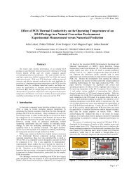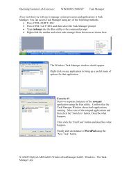
8051 Serial Port - gmitWEB
8051 Serial Port - gmitWEB
8051 Serial Port - gmitWEB

Create successful ePaper yourself
Turn your PDF publications into a flip-book with our unique Google optimized e-Paper software.
<strong>8051</strong> <strong>Serial</strong> <strong>Port</strong><br />
• The <strong>8051</strong> contains a UART – Universal Asynchronous Receiver Transmitter<br />
– The serial port is full-duplex<br />
• It can transmit and receive simultaneously<br />
– 2 <strong>Port</strong> 3 pins are used to provide the serial interface<br />
• P3.0 is the receive pin (RXD)<br />
• P3.1 is the transmit pin (TXD)<br />
– Both synchronous and asynchronous transmission supported<br />
• A synchronous transmission sends a clock signal with the data<br />
– Adjustable baud rate and data frame size supported in asynchronous mode<br />
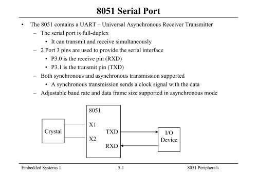
<strong>8051</strong><br />
Crystal<br />
X1<br />
X2<br />
TXD<br />
RXD<br />
I/O<br />
Device<br />
Embedded Systems 1 5-1 <strong>8051</strong> Peripherals
Asynchronous Data Transmission<br />
• Data is transmitted in a frame consisting of a start bit, 8 or 9 data bits and a stop bit<br />
– Start bit is always low<br />
– Data is transmitted LSB first<br />
– Stop bit is always high<br />
• Data transmission/reception rate is controlled by baud rate generator clock<br />
– Baud rate may be a division of the crystal frequency or programmed using a<br />
timer<br />
D0 D1 D2 D3 D4 D5 D6 D7<br />
Line Idle<br />
Start Bit<br />
Stop Bit<br />
Embedded Systems 1 5-2 <strong>8051</strong> Peripherals
<strong>Serial</strong> <strong>Port</strong> Modes<br />
• Mode 0<br />
– Only synchronous mode<br />
– Data transferred on RXD, clock on TXD<br />
– Clock is fixed at 1/12 of the oscillator frequency<br />
• Mode 1<br />
– Asynchronous mode<br />
– 10-bit data frame (start bit, 8 data bits and a stop bit)<br />
– Variable baud rate<br />
– Stop bit is placed in RB8 bit of SCON register on reception of a frame<br />
Embedded Systems 1 5-3 <strong>8051</strong> Peripherals
<strong>Serial</strong> <strong>Port</strong> Modes<br />
• Mode 2<br />
– Asynchronous mode<br />
– 11-bit data frame (start bit, 8 data bits, programmable 9 th bit and a stop bit)<br />
– On transmission 9 th bit is TB8 bit of SCON<br />
– On reception 9 th bit is placed in RB8 bit of SCON<br />
– 9 th bit may be used for data or as a parity bit<br />
– Baud rate may be 1/32 or 1/64 of oscillator frequency<br />
• Mode 3<br />
– Same as Mode 2 but with a programmable baud rate<br />
Embedded Systems 1 5-4 <strong>8051</strong> Peripherals
Data Transmission/Reception<br />
• The register SBUF is used to hold both the transmit and receive serial port data<br />
• To transmit data load the SBUF register<br />
– MOV SBUF, source<br />
– When transmission is complete the TI bit will be set in the SCON register<br />
• When a data frame is received the RI bit in SCON is set high<br />
– The received data may then be loaded from SBUF<br />
– MOV destination, SBUF<br />
– Data reception is double buffered<br />
• Reception of a second data frame may commence before the previous data<br />
frame has been read<br />
– The REN bit in SCON must be set to enable data reception<br />
Embedded Systems 1 5-5 <strong>8051</strong> Peripherals
SCON Register<br />
Embedded Systems 1 5-6 <strong>8051</strong> Peripherals
Configuring the <strong>Serial</strong> <strong>Port</strong><br />
• Configure the serial port mode in SCON<br />
– Bits SM0 and SM1 determine the mode<br />
– Set the REN bit if serial data reception is required<br />
– Clear the RI and TI bits<br />
• The RI flag is set when a character has been received by the serial port<br />
• The TI flag is set after transmission of a character<br />
• Both flags must be cleared by software<br />
• Configure the serial port baud rates<br />
– The baud rate is fixed for modes 0 and 2<br />
• For mode 0 the baud rate = f osc<br />
/12<br />
• For mode 2 the baud rate = 2 SMOD * f osc<br />
/64<br />
– SMOD is a bit in the PCON register (not bit addressable)<br />
– For modes 1 and 3 the baud rate is configured by the timer 1 overflow rate<br />
Embedded Systems 1 5-7 <strong>8051</strong> Peripherals
Baud Rate for Modes 1 and 3<br />
• Configure timer 1 for 8-bit auto-reload mode (timer mode 2)<br />
– Upper 4 bits of TMOD register = 0010<br />
Baud Rate<br />
=<br />
2<br />
32<br />
SMOD<br />
x<br />
( Timer 1Overflow Rate)<br />
Baud Rate<br />
=<br />
2<br />
32<br />
SMOD<br />
x<br />
Oscillator Frequency<br />
12x<br />
[ 256 − TH1]<br />
Embedded Systems 1 5-8 <strong>8051</strong> Peripherals
Common Baud Rates<br />
Embedded Systems 1 5-9 <strong>8051</strong> Peripherals
<strong>Serial</strong> Program Example 1<br />
;Program to continually transmit the character A out the serial port<br />
ORG 0H<br />
MOV SCON, #40H ;serial port mode 1<br />
;configure timer 1 in auto-reload mode for 9600 baud<br />
MOV TMOD, #20H ;timer mode 2<br />
MOV TH1, #0FDH ;reload value for 9600 baud<br />
MOV TL1, #0FDH<br />
SETB TR1<br />
;start timer<br />
LOOP: MOV SBUF, #'A' ;transmit character<br />
WAIT4TI: JNB TI, WAIT4TI ;wait for end of transmission<br />
CLR TI<br />
JMP LOOP ;re-transmit<br />
END<br />
Embedded Systems 1 5-10 <strong>8051</strong> Peripherals
<strong>Serial</strong> Program Example 2<br />
; Program to echo characters received on serial port<br />
ORG 0H<br />
MOV SCON, #50H ;serial port mode 1, receiver enabled<br />
ORL PCON, #80H ;SMOD = 1, double baud rate<br />
;configure timer 1 in auto-reload mode for 19200 baud<br />
MOV TMOD, #20H ;timer mode 2<br />
MOV TH1, #0FDH ;reload value for 19200 baud with SMOD = 1<br />
MOV TL1, #0FDH<br />
SETB TR1<br />
;start timer<br />
;wait for a character to be received<br />
WAIT4RI: JNB RI, WAIT4RI ;wait for receive flag to go high<br />
CLR RI<br />
MOV A, SBUF<br />
;read received character<br />
;transmit received character<br />
MOV SBUF, A<br />
;transmit character<br />
WAIT4TI: JNB TI, WAIT4TI ;wait for end of transmission<br />
CLR TI<br />
JMP WAIT4RI<br />
;return and wait for next character<br />
END<br />
Embedded Systems 1 5-11 <strong>8051</strong> Peripherals
<strong>Serial</strong> Program Example 3<br />
;Program to print the message "Hello" "Goodbye" on serial port<br />
;A new line is placed between the strings<br />
MESSAGE EQU 100H<br />
;address where string is stored<br />
;define characters to move cursor to next line<br />
CR EQU 0DH<br />
LF EQU 0AH<br />
ORG 0H<br />
MOV SCON, #40H ;serial port mode 1<br />
;configure timer 1 in auto-reload mode for 9600 baud<br />
MOV TMOD, #20H ;timer mode 2<br />
MOV TH1, #0FDH ;reload value for 9600<br />
MOV TL1, #0FDH<br />
SETB TR1<br />
;start timer<br />
;continued on next slide<br />
Embedded Systems 1 5-12 <strong>8051</strong> Peripherals
<strong>Serial</strong> Program Example 3 (cont)<br />
;loop to transmit message<br />
MOV DPTR, #MESSAGE<br />
TXMSG: CLR A<br />
MOVC A, @A+DPTR ;fetch character from string<br />
CJNE A, #'*', TRANSMIT ;check for end of message<br />
JMP DONE<br />
TRANSMIT: MOV SBUF, A ;transmit character<br />
WAIT4TI: JNB TI, WAIT4TI ;wait for end of transmission<br />
CLR TI<br />
INC DPTR<br />
;point to next character<br />
JMP TXMSG<br />
DONE:<br />
ORG MESSAGE<br />
DB 'Hello'<br />
DB CR, LF<br />
DB 'Goodbye*'<br />
END<br />
;string to be printed<br />
Embedded Systems 1 5-13 <strong>8051</strong> Peripherals
Synchronous <strong>Serial</strong> Comms (Mode 0)<br />
• The TXD pin is used to carry the clock<br />
• Data is transmitted and received on the RXD pin (half duplex)<br />
• Data Transmission<br />
– Initiated by writing a character to the SBUF register<br />
– Data shifted out RXD pin, LSB first (8 bits in total)<br />
– 8 clocks shifted out TXD pin<br />
– TI flag set after byte of data has been transmitted<br />
• Data Reception<br />
– Initiated by REN = 1 and RI = 0<br />
– 8 clock pulses are outputted on TXD pin<br />
– 1 bit of data shifted into RXD pin for each clock<br />
– RI is set when 8 bits have been received into SBUF<br />
Embedded Systems 1 5-14 <strong>8051</strong> Peripherals
<strong>Serial</strong> I/O Expansion<br />
• A 74LS164 <strong>Serial</strong> In Parallel Out Shift Register may be used to expand the serial port<br />
to be used as 8 output pins<br />
– A number of shift registers may be cascaded to increase the number of output<br />
pins gained<br />
Data Input<br />
Clock<br />
Reset<br />
8 Parallel Outputs<br />
Embedded Systems 1 5-15 <strong>8051</strong> Peripherals
<strong>Serial</strong> Output Pin Expansion<br />
• P1.0 will clear the shift register outputs when brought low<br />
• 8 output pins generated from 3 <strong>8051</strong> pins<br />
– Connect Q7 of 74LS164 to the data input of a second 74LS164 to generate 15<br />
outputs from 3 <strong>8051</strong> pins<br />
<strong>8051</strong><br />
74LS164<br />
P1.0<br />
RXD<br />
TXD<br />
MR<br />
DIN<br />
CLK<br />
Q0<br />
Q1<br />
Q2<br />
Q3<br />
Q4<br />
Q5<br />
Q6<br />
Q7<br />
8 Output<br />
<strong>Port</strong>s<br />
Embedded Systems 1 5-16 <strong>8051</strong> Peripherals
<strong>Serial</strong> Input Pin Expansion<br />
• A 74LS165 Parallel In <strong>Serial</strong> Out Shift Register may be used to allow the <strong>8051</strong> serial<br />
port to provide additional input port pins<br />
– A number of shift registers may be cascaded to increase the number of output<br />
pins gained<br />
Embedded Systems 1 5-17 <strong>8051</strong> Peripherals
<strong>Serial</strong> Input Pin Expansion<br />
• P1.0 will load the register parallel inputs when brought low<br />
• 8 input pins generated from 3 <strong>8051</strong> pins<br />
– Connect data output pin of a second 74LS165 to the data input pin of another to<br />
generate 16 inputs from 3 <strong>8051</strong> pins<br />
74LS165<br />
8 Input<br />
<strong>Port</strong>s<br />
QA<br />
QB<br />
QC<br />
QD<br />
QE<br />
QF<br />
QG<br />
QH<br />
INHIB<br />
OUT<br />
CLK<br />
LOAD<br />
<strong>8051</strong><br />
RXD<br />
TXD<br />
P1.0<br />
INPUT<br />
Embedded Systems 1 5-18 <strong>8051</strong> Peripherals
Multi-Processor Communication<br />
• Modes 2 and 3 can be configured to allow serial communication between a master<br />
<strong>8051</strong> and a number of slave <strong>8051</strong>s<br />
– The TXD pin of the master connects to the RXD pin of the slave <strong>8051</strong>s<br />
– In modes 2 and 3 a 9 th data bit is transmitted<br />
• This bit is received into the RB8 bit of the SCON register<br />
• If the SM2 bit of SCON is set, the RI flag will only be set when a serial<br />
frame is received with the 9 th bit = ‘1’<br />
• This 9 th bit can be set/cleared to specify an address/data frame<br />
TXD<br />
Master<br />
<strong>8051</strong><br />
RXD<br />
RXD<br />
RXD<br />
Slave<br />
<strong>8051</strong> #1<br />
Slave<br />
<strong>8051</strong> #2<br />
…………..<br />
Slave<br />
<strong>8051</strong> #n<br />
Embedded Systems 1 5-19 <strong>8051</strong> Peripherals
Multi-Processor Communication<br />
• On initialisation all slaves set the SM2 bit in the SCON register<br />
– Each slave has a unique 8-bit address stored in non-volatile memory<br />
• Master <strong>8051</strong> sends an address frame – 9 th bit TB8 = ‘1’<br />
– The address frame contains the 8-bit address of the destination slave<br />
• All slaves will see the received address frame<br />
– RI bit will be set because the 9 th bit RB8 = ‘1’<br />
– Each slave checks the received address against it’s own address<br />
• The addressed slave will now clear it’s SM2 bit in SCON to ‘0’<br />
• The master will now send some data frames with the 9 th bit = ‘0’<br />
– Only the addressed slave will see the data frames<br />
– No RI flag will be set in the other slaves because the RB8 bit is ‘0’<br />
– On completion of data reception the addressed slave will set the SM2 bit to await<br />
another address frame<br />
Embedded Systems 1 5-20 <strong>8051</strong> Peripherals