Photonic Crystals: Semiconductors of Light - Yablonovitch Research ...
Photonic Crystals: Semiconductors of Light - Yablonovitch Research ...
Photonic Crystals: Semiconductors of Light - Yablonovitch Research ...

You also want an ePaper? Increase the reach of your titles
YUMPU automatically turns print PDFs into web optimized ePapers that Google loves.
Copyright 2001 Scientific American, Inc.
PHOTONIC<br />
CRYSTALS:<br />
SEMICONDUCTORS<br />
OF LIGHT<br />
By Eli <strong>Yablonovitch</strong><br />
Nanostructured materials containing<br />
ordered arrays <strong>of</strong> holes could lead to<br />
an optoelectronics revolution, doing<br />
for light what silicon did for electrons<br />
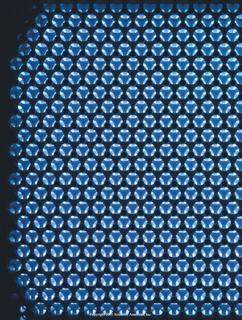
FIRST SUCCESSFUL PHOTONIC CRYSTAL was formed by drilling three<br />
intersecting arrays <strong>of</strong> holes into a block <strong>of</strong> a ceramic material. Each array<br />
is angled 35 degrees from vertical (into the page), producing a structure<br />
now called yablonovite. The pattern <strong>of</strong> six-millimeter-diameter holes blocks<br />
radio waves from 13 to 16 gigahertz.<br />
Copyright 2001 Scientific American, Inc.<br />
SCIENTIFIC AMERICAN 47
IT WAS THE SECOND EXASPERATING PHONE CALL THAT I HAD RECEIVED.<br />
Yet another group <strong>of</strong> theorists was saying that my discovery did not work. That was<br />
distressing. I had spent three long years trying and discarding countless designs<br />
to arrive at what I thought was success, but if the theorists were right, I had to go<br />
back to the lab and continue searching. And maybe what I was trying to create—<br />
an artificial crystal structure that could<br />
manipulate beams <strong>of</strong> light in the same<br />
way that silicon and other semiconductors<br />
control electric currents—was not<br />
possible at all.<br />
Electronic semiconductors, <strong>of</strong> course,<br />
are at the heart <strong>of</strong> all the computers and<br />
other devices that pervade the global economy.<br />
<strong>Semiconductors</strong> <strong>of</strong> light could lead<br />
the information and telecommunications<br />
Overview/<strong>Photonic</strong> <strong>Crystals</strong><br />
revolution still further by enabling highercapacity<br />
optical fibers, nanoscopic lasers<br />
and photonic integrated circuits that<br />
might one day replace today’s microchips.<br />
Indeed, despite a rocky start in the late<br />
1980s and much skepticism from the<br />
photonics research community early on,<br />
the field <strong>of</strong> photonic crystals has thrived.<br />
Around the world many researchers (including<br />
me) have founded companies that<br />
■ The microelectronics and information revolution is based on the elaborate<br />
control <strong>of</strong> electric currents achieved with semiconductors such as silicon. That<br />
control depends on a phenomenon called the band gap: a range <strong>of</strong> energies in<br />
which electrons are blocked from traveling through the semiconductor.<br />
■ Scientists have produced materials with a photonic band gap—a range <strong>of</strong><br />
wavelengths <strong>of</strong> light that is blocked by the material—by structuring the<br />
materials in carefully designed patterns at the nanoscopic-size scale. These<br />
photonic crystals function as “semiconductors for light” and promise<br />
innumerable technological applications.<br />
■ Many researchers greeted the idea <strong>of</strong> a photonic band gap with skepticism and<br />
disinterest when it was first proposed, but today photonic crystals are rapidly<br />
turning into big business. <strong>Photonic</strong> crystals have applications such as highcapacity<br />
optical fibers, color pigments and photonic integrated circuits that<br />
would manipulate light in addition to electric currents.<br />
are developing commercial products. The<br />
key was proving the skeptics wrong by<br />
showing that it was possible to create for<br />
light the same kind <strong>of</strong> phenomenon seen<br />
in electronic semiconductors—namely, a<br />
so-called band gap.<br />
The electronic band gap is a forbidden<br />
zone, a narrow range <strong>of</strong> energies that electrons<br />
cannot occupy. When the electrons<br />
in the semiconductor fill all the states<br />
available to them below the band gap,<br />
electric current cannot flow, because each<br />
electron has nowhere to go. Boosting an<br />
electron above the gap takes a lot <strong>of</strong> energy.<br />
If there are a few excess electrons,<br />
however, they automatically must sit<br />
above the gap, where they can easily roam<br />
through the wide open spaces <strong>of</strong> empty<br />
states. Similarly, a deficit <strong>of</strong> electrons<br />
opens up some positively charged “holes”<br />
below the gap, again providing a way for<br />
current to flow readily.<br />
All the magic <strong>of</strong> semiconductors—the<br />
switching and logic functions—comes<br />
about from controlling the availability <strong>of</strong><br />
electrons and holes above and below the<br />
band gap. The existence and properties <strong>of</strong><br />
an electronic band gap depend crucially<br />
COURTESY OF ELI YABLONOVITCH (preceding pages)<br />
48 SCIENTIFIC AMERICAN DECEMBER 2001<br />
Copyright 2001 Scientific American, Inc.
OPTICAL FIBERS can use the photonic band-gap principle to guide light.<br />
The cladding <strong>of</strong> several hundred silica capillary tubes forms an optical<br />
band-gap material that confines light to the central hole, which is about<br />
15 microns in diameter (left). In the design at the right, in which the light is<br />
confined to the two-micron solid core, the fiber is highly nonlinear, which<br />
can be useful for switching and shaping light pulses. In the center, a<br />
pattern <strong>of</strong> colors illustrates how the confinement property <strong>of</strong> a band-gap<br />
fiber varies for different wavelengths <strong>of</strong> light.<br />
COURTESY OF BLAZE PHOTONICS (left and center); CRYSTAL FIBRE A/S (right)<br />
on the type <strong>of</strong> atoms in the material and<br />
their crystal structure—the spacing and<br />
shape <strong>of</strong> the lattice that they form. By substituting<br />
various other atoms (called<br />
dopants) into the lattice or its interstices,<br />
engineers can dictate the number <strong>of</strong> electrons<br />
or holes in the semiconductor and<br />
thereby tailor its properties.<br />
In silicon and other semiconductors,<br />
adjacent atoms are separated by about a<br />
quarter <strong>of</strong> a nanometer. <strong>Photonic</strong> bandgap<br />
materials involve similar structures<br />
but at larger scales. A typical example<br />
would be a block <strong>of</strong> special glass drilled<br />
through with a closely spaced array <strong>of</strong><br />
cylindrical holes, each with a diameter <strong>of</strong><br />
400 nanometers. These openings are analogous<br />
to the atoms in a semiconductor. In<br />
general, but not always, the spacing <strong>of</strong> the<br />
array must be reasonably close to the<br />
wavelength <strong>of</strong> the light or the electromagnetic<br />
waves to be controlled. Visible light<br />
has wavelengths ranging from about 400<br />
to 700 nanometers; many cell phones use<br />
waves around 35 centimeters long.<br />
<strong>Light</strong> entering the holey material will<br />
refract through and partially reflect <strong>of</strong>f<br />
the myriad internal interfaces between air<br />
and glass. The complex pattern <strong>of</strong> overlapping<br />
beams will reinforce or cancel<br />
one another out according to the light’s<br />
wavelength, its direction <strong>of</strong> travel through<br />
the crystal, the refractive index <strong>of</strong> the<br />
glass, and the size and arrangement <strong>of</strong> all<br />
the holes. Perfect cancellation in all directions<br />
for a narrow band <strong>of</strong> wavelengths<br />
is like the band gap for electrons<br />
in semiconductors: that band <strong>of</strong> light<br />
cannot propagate through the crystal.<br />
Modifying the band gap structure—for<br />
instance, by filling some holes—produces<br />
other effects, similar to what can be done<br />
by doping electronic semiconductors. Often<br />
a photonic crystal is made <strong>of</strong> an electronic<br />
semiconductor material, and so<br />
the crystal has both an electronic band<br />
gap and a photonic band gap.<br />
500,000 Holes<br />
THE QUEST for a photonic band gap<br />
originated quietly enough in 1987 with<br />
two independent proposals submitted for<br />
publication just two months apart: one by<br />
me and the other by Sajeev John, then at<br />
Princeton University. We had two very<br />
different goals in mind. I was at Bell Communications<br />
<strong>Research</strong>, the telephone research<br />
consortium in New Jersey, and I<br />
was seeking to make telecommunications<br />
lasers more efficient. Most <strong>of</strong> the electric<br />
current consumed to produce lasing was<br />
wasted as spontaneous light emission,<br />
and the photonic band gap could suppress<br />
that waste: atoms cannot spontaneously<br />
emit light when they are part <strong>of</strong><br />
THE AUTHOR<br />
a material that forbids light propagation.<br />
John, in contrast, was pursuing a<br />
pure research goal. He proposed the photonic<br />
band gap to create what is known<br />
as light localization. The electronic analogue<br />
<strong>of</strong> this phenomenon, a quantum effect<br />
called electron localization, occurs in<br />
disordered materials such as amorphous<br />
semiconductors. The disorder traps, or<br />
localizes, electrons in fixed locations, obstructing<br />
current flow.<br />
John and I had never met, but when<br />
we learned <strong>of</strong> each other’s proposal, we<br />
were curious enough to arrange a getacquainted<br />
lunch. We thought we were<br />
onto something, and we agreed to use the<br />
same terminology: “photonic band gap”<br />
and “photonic crystal.” I returned to my<br />
lab rather overconfident. I thought that<br />
I might create the first working model<br />
within only a few months.<br />
Although “photonic” refers to light,<br />
the principle <strong>of</strong> the band gap applies<br />
equally well to electromagnetic waves <strong>of</strong><br />
all wavelengths. Consequently, I could<br />
make trial crystal structures with any convenient<br />
row spacing and size and then test<br />
them with electromagnetic waves <strong>of</strong> the<br />
appropriate wavelength. Indeed, I began<br />
ELI YABLONOVITCH was an inventor <strong>of</strong> the photonic band-gap concept and made the first<br />
photonic band-gap crystal while at Bell Communications <strong>Research</strong> in New Jersey. In 1992<br />
he moved to the electrical engineering department at the University <strong>of</strong> California, Los Angeles,<br />
where he leads the optoelectronics group. He is a founder <strong>of</strong> two companies in the<br />
burgeoning field <strong>of</strong> photonic crystals: Ethertronics and Luxtera. Before he became a faculty<br />
member, <strong>Yablonovitch</strong> had enough time to sail racing sloops.<br />
www.sciam.com SCIENTIFIC AMERICAN 49<br />
Copyright 2001 Scientific American, Inc.
my quest for a photonic band-gap material<br />
in a machine shop, carving structures<br />
out <strong>of</strong> dielectric plates with a drill. Only<br />
human imagination limited the crystal design<br />
and structure. Therein lay a problem,<br />
however. Out <strong>of</strong> the innumerable choices<br />
available, which design would produce a<br />
photonic band gap?<br />
In electronic semiconductor crystals,<br />
the band gap arises because electrons behave<br />
partly like a wave, and the waves<br />
scatter <strong>of</strong>f the layers or rows <strong>of</strong> atoms.<br />
Part <strong>of</strong> the wave scatters back the way it<br />
came, and if the wavelength is about the<br />
same as the spacing <strong>of</strong> successive layers,<br />
all the backscattered waves add up coherently.<br />
Consequently, the electron’s<br />
wave is reflected back completely, like<br />
light hitting a mirror. For a full band gap,<br />
this perfect reflection must occur over a<br />
range <strong>of</strong> wavelengths and for waves heading<br />
in any direction through the crystal.<br />
physical intuition as calculations, my coworkers<br />
and I built structure after structure,<br />
searching for the right one. In the<br />
course <strong>of</strong> four years, my loyal machinist,<br />
John Gural, drilled more than 500,000<br />
holes in dielectric (insulating) plates, admittedly<br />
assisted by a numerically controlled<br />
machine. It became unnerving as<br />
we produced failure after failure.<br />
The Surprise <strong>of</strong> Diamond<br />
WE EXPECTED the face-centered cubic<br />
(fcc) structure to be particularly favorable<br />
for making electromagnetic band<br />
gaps. You can build this structure by taking<br />
a checkerboard and placing a black<br />
cube on each white square and a white<br />
one on each black square. On the second<br />
layer, continue placing black cubes on<br />
white and vice versa, and so on up. The<br />
black cubes (and separately also the<br />
white ones) form an fcc lattice.<br />
Unlike lattices <strong>of</strong> atoms, photonic crystals have<br />
structural possibilities limited only by the human imagination.<br />
Any shape can be sculpted at the lattice sites.<br />
For an electromagnetic band gap, I<br />
knew one could not simply emulate a silicon<br />
crystal. For light, the scattering is<br />
caused by changes <strong>of</strong> refractive index (for<br />
instance, between air and glass), and an<br />
interaction directly analogous to electrons<br />
and silicon atoms would require a<br />
material with an extraordinary refractive<br />
index.<br />
Nor could one simply deduce a structure<br />
from theory: the band gap depends<br />
on how the waves interact with many<br />
hundreds <strong>of</strong> holes, a very complicated<br />
process. Theorists had developed computer<br />
models for doing the calculations<br />
for semiconductors, but these programs<br />
could not be used for photons. First, the<br />
equations <strong>of</strong> motion are different—Schrödinger’s<br />
equation governs electrons, but<br />
Maxwell’s equations describe the behavior<br />
<strong>of</strong> light. Second, with photons one<br />
cannot safely neglect polarization the way<br />
one can with electrons. Consequently, I<br />
had no way to determine whether a proposed<br />
structure would have a photonic<br />
band gap. And so, guided as much by<br />
That structure still leaves an infinite<br />
variety <strong>of</strong> choices because you can substitute<br />
any other geometric shape for the<br />
black cubes, which alters how the light<br />
waves will be refracted and reflected. After<br />
two years, we arrived at something<br />
that seemed to work: an fcc structure in<br />
which each black cube was replaced by a<br />
spherical void in the material. I published<br />
this result, but I was mistaken.<br />
By now the theorists had started to<br />
catch up, and a few <strong>of</strong> them had retooled<br />
their band-structure computer programs<br />
to work with light. Several theory groups,<br />
including those led by K. Ming Leung <strong>of</strong><br />
Polytechnic University and Kai Ming Ho<br />
<strong>of</strong> Iowa State University, began making<br />
those dreaded phone calls. My longsought<br />
fcc structure had only a pseudogap:<br />
a forbidden “band” having zero<br />
width, meaning that just one exact wavelength<br />
<strong>of</strong> light was forbidden. After our<br />
years <strong>of</strong> effort, it appeared that nature<br />
might not permit a photonic band gap to<br />
exist at all. Perhaps it required a substance<br />
with a refractive index far beyond<br />
that <strong>of</strong> any existing transparent material.<br />
Within weeks, however, the Iowa<br />
State group found that the diamond<br />
structure, the tetrahedral crystal geometry<br />
associated with the precious jewel,<br />
would produce a band gap. The form<br />
that gives the widest band gap consists <strong>of</strong><br />
dielectric rods in the positions <strong>of</strong> the<br />
chemical bonds between carbon atoms,<br />
with the atoms shrunk to geometric<br />
points. Diamond itself is not a photonic<br />
band-gap material, as far as we know.<br />
Earlier in this piece I said that when we<br />
began our research, we knew we could<br />
not simply emulate the silicon crystal<br />
structure to produce a photonic band<br />
gap. How wrong we were: silicon’s crystal<br />
structure is precisely that <strong>of</strong> diamond.<br />
That the tetrahedral structure is the<br />
best for making a photonic band gap is<br />
startling and pr<strong>of</strong>ound. Before the advent<br />
<strong>of</strong> photonic crystals, the diamond configuration<br />
was merely another mineral<br />
structure, arising out <strong>of</strong> a complex interplay<br />
<strong>of</strong> atoms, chemical bonds and energy<br />
minimization under suitable conditions<br />
<strong>of</strong> temperature and pressure. Its utility<br />
for forming a photonic band gap,<br />
which emerges entirely and solely from<br />
Maxwell’s equations (the laws <strong>of</strong> electricity,<br />
magnetism and light), shows that<br />
the diamond configuration also has fundamental<br />
significance in relation to electromagnetism<br />
and the geometry <strong>of</strong> threedimensional<br />
space.<br />
Diamond’s tetrahedral structure takes<br />
on many different appearances according<br />
to what shape is placed in each lattice site<br />
and from which angle the crystal is<br />
viewed. The box on the opposite page includes<br />
two very dissimilar photonic crystals<br />
that are based on the diamond structure.<br />
My group made the first successful<br />
photonic band-gap crystal (this time for<br />
real) in 1991 using a variant <strong>of</strong> the diamond<br />
structure now called yablonovite.<br />
Nature is kind after all: a band gap occurs<br />
in the diamond structure for a refractive<br />
50 SCIENTIFIC AMERICAN DECEMBER 2001<br />
Copyright 2001 Scientific American, Inc.
ONE DIMENSION<br />
FOR WAVELENGTH IN BAND GAP<br />
MAKING BAND GAPS IN ALL DIMENSIONS<br />
A wave incident on a band-gap material (1) partially reflects <strong>of</strong>f each layer <strong>of</strong> the structure<br />
(2). The reflected waves are in phase and reinforce one another. They combine with the<br />
incident wave to produce a standing wave (3) that does not travel through the material.<br />
1<br />
1 INCIDENT WAVE<br />
DIELECTRIC SLAB<br />
2 REFLECTED WAVES IN PHASE<br />
2<br />
3 TOTAL WAVE<br />
FOR WAVELENGTH NOT IN BAND GAP<br />
At a wavelength outside the band gap (1), the reflected waves are out <strong>of</strong> phase and cancel<br />
out one another (2). The light propagates through the material only slightly attenuated (3).<br />
3<br />
1 INCIDENT WAVE<br />
2 REFLECTED WAVES NOT IN PHASE<br />
4<br />
3 TOTAL WAVE<br />
SLIM FILMS<br />
TWO DIMENSIONS<br />
For a two-dimensional band gap, each unit cell <strong>of</strong> the structure (1) produces reflected<br />
waves (not shown) and refracted waves that must combine to cancel out the incoming<br />
wave (2) no matter what direction it is traveling (3). A full three-dimensional band-gap<br />
material works the same way but in all three dimensions.<br />
1 2 3<br />
THREE DIMENSIONS<br />
Diamond’s tetrahedral configuration (1) is<br />
the most effective geometry for making threedimensional<br />
band-gap materials. This geometry<br />
occurs in disguised form in yablonovite (see pages<br />
46 and 47), the “stack <strong>of</strong> logs” (2), and this design<br />
(3), which uses silicon dioxide channels (light)<br />
in silicon (dark). The scaffold structure (4) is<br />
a rare example that has a different underlying<br />
symmetry, but it has only a small band gap.<br />
Copyright 2001 Scientific American, Inc.
index as small as 1.87, and many optical<br />
materials are available with refractive indices<br />
as high as 3.6.<br />
The diamond structure isn’t the only<br />
structure having a photonic band gap. In<br />
1992 theorist Joseph W. Haus, then at<br />
Rensselaer Polytechnic Institute, showed<br />
that we had discarded the fcc structures<br />
too quickly. Scientists had searched the<br />
fcc structures for band gaps only at wavelengths<br />
for which about half a wave fits<br />
Butterflies and Microchips<br />
WE HAVE NOW LEARNED that nature<br />
already makes photonic crystals in the<br />
sparkling gem opal, in a butterfly’s colorful<br />
wings and in the hairs <strong>of</strong> a wormlike<br />
creature called the sea mouse. Each<br />
<strong>of</strong> these has a photonic band structure,<br />
though not a full band gap, in that light<br />
can still propagate in some directions. A<br />
complete band gap has eluded nature,<br />
perhaps because it requires too much refractive-index<br />
contrast.<br />
Nevertheless, an incomplete band<br />
gap can be very useful. For example, titanium<br />
dioxide particles smaller than a<br />
core, which confines light by total internal<br />
reflection. Philip St. J. Russell <strong>of</strong> the<br />
University <strong>of</strong> Bath in England demonstrated<br />
in 1999 how to make photonic<br />
band-gap fibers. In one version, light<br />
travels along a central hole in the fiber,<br />
confined there by the two-dimensional<br />
band gap <strong>of</strong> the surrounding material.<br />
More optical power can be sent through<br />
such a central void than through glass,<br />
enabling greater information-carrying<br />
Integrated circuits that combine<br />
conventional electronics and photonic crystals would represent<br />
the ultimate limit <strong>of</strong> optoelectronic miniaturization.<br />
in one cell <strong>of</strong> the lattice (somewhat like<br />
the fundamental vibration <strong>of</strong> a guitar<br />
string). As we saw, only a pseudo-gap occurs<br />
at that frequency. Haus, however,<br />
also considered a higher frequency, for<br />
which a full wavelength fits in a cell<br />
(somewhat like the first harmonic <strong>of</strong> the<br />
guitar string), and proved that an fcc<br />
band gap would indeed emerge there. In<br />
addition, he discovered that even the simple<br />
cubic configuration known as the<br />
scaffold structure (for its similarity to<br />
scaffolding) could have a band gap, albeit<br />
a small one.<br />
micron can be made to self-assemble in<br />
the opal structure. Titanium dioxide is<br />
the intensely white pigment used in paint<br />
and to make paper white. The coherent<br />
scattering <strong>of</strong> light that occurs from bandgap-structured<br />
titanium dioxide can impart<br />
more whiteness for less mass <strong>of</strong> titanium<br />
dioxide. One day photonic crystals<br />
may be all around us in the painted<br />
walls and in the stacks <strong>of</strong> paper cluttering<br />
our desks.<br />
Another very useful type <strong>of</strong> incomplete<br />
band gap material is that <strong>of</strong> two-dimensional<br />
photonic crystals, which can<br />
block light from traveling within a plane.<br />
Such a structure can be stretched along<br />
the third dimension, forming a new kind<br />
<strong>of</strong> optical fiber. Conventional optical<br />
fibers have a high refractive index at their<br />
APPLICATIONS FORPHOTONICCRYSTALS<br />
DEVICE<br />
OPTICAL FIBERS<br />
DESCRIPTION<br />
2-D band-gap material stretched along the third dimension<br />
capacity, perhaps 100 times that <strong>of</strong> conventional<br />
telecommunications fibers.<br />
Specialty fibers have advanced the most<br />
as commercial photonic band-gap products.<br />
Companies in Denmark and the<br />
U.K. have already distributed sample<br />
quantities and will soon begin volume<br />
production.<br />
Instead <strong>of</strong> stretching out a two-dimensional<br />
band-gap structure to make a<br />
fiber, one can go to the other extreme and<br />
make a two-dimensional thin-film photonic<br />
crystal, as was first calculated in<br />
1997 by Shanhui Fan and John D.<br />
Joannopoulos, then both at the Massachusetts<br />
Institute <strong>of</strong> Technology. Thinfilm<br />
photonic crystals can be easily patterned<br />
by standard methods used to produce<br />
integrated circuits. Introducing<br />
STATUS<br />
Early versions already commercialized<br />
NANOSCOPIC LASERS<br />
ULTRAWHITE PIGMENT<br />
RADIO-FREQUENCY<br />
ANTENNAS, REFLECTORS<br />
LIGHT-EMITTING DIODES<br />
PHOTONIC INTEGRATED<br />
CIRCUITS<br />
World’s tiniest optical cavities and tiniest lasers;<br />
formed in a thin-film 2-D band-gap material<br />
Incomplete 3-D band-gap material, usually patterned<br />
as opal structure<br />
Uses inductors and capacitors in place <strong>of</strong> ordinary<br />
dielectric materials<br />
<strong>Photonic</strong> band-gap structure can extract light very efficiently<br />
(better than 50%)<br />
2-D thin films can be patterned like conventional integrated<br />
circuits to make channel filters, modulators, couplers and so on<br />
Demonstrated in the lab<br />
Demonstrated; low-cost manufacturing<br />
methods under development<br />
Demonstrated for magnetic resonance<br />
imaging and antennas<br />
Demonstrated, but must compete with<br />
other methods <strong>of</strong> achieving the same goal<br />
Under development<br />
54 SCIENTIFIC AMERICAN DECEMBER 2001<br />
Copyright 2001 Scientific American, Inc.
NATURAL PHOTONIC BAND GAPS occur in some butterfly wings (left) and in<br />
opals (right). In both cases, the band gap is incomplete—it is not effective<br />
in every direction—but it produces iridescent colors. A micrograph <strong>of</strong> a<br />
fractured iridescent green butterfly scale (center) shows the submicronsize<br />
face-centered cubic structure inside. Opals consist <strong>of</strong> submicron-size<br />
silica spheres arranged in a face-centered cubic (close-packed) structure.<br />
PAUL BEARD (left); HELEN GHIRADELLA, FROM THE ANNALS OF THE ENTOMOLOGICAL<br />
SOCIETY OF AMERICA, VOL. 78, 1985 (center); THE PURCELL TEAM Corbis ( right)<br />
defects to a band-gap structure is comparable<br />
to doping in an electronic semiconductor<br />
and opens up a vast range <strong>of</strong><br />
functions. One example <strong>of</strong> a dopant is<br />
the central hole in photonic crystal optical<br />
fibers. Similarly, plugging one <strong>of</strong> the<br />
holes in a thin-film crystal produces a<br />
critical element <strong>of</strong> lasers, namely a small<br />
“cavity” that can hold a local electromagnetic<br />
mode—imagine a little standing<br />
wave <strong>of</strong> light trapped between mirrors.<br />
Recently Axel Scherer’s group at the California<br />
Institute <strong>of</strong> Technology used these<br />
tiniest <strong>of</strong> optical cavities to make lasers<br />
just 0.03 cubic micron in volume, the<br />
smallest ever.<br />
Patterning photonic crystal thin films<br />
into optical circuits would represent the<br />
ultimate limit <strong>of</strong> optoelectronic miniaturization.<br />
Many researchers believe that<br />
integrated circuits that combine conventional<br />
electronics and photonics stand<br />
ready to extend the integrated-circuit revolution<br />
into the domain <strong>of</strong> high-bandwidth<br />
optical signals. This field <strong>of</strong> bandgap<br />
device development will probably<br />
draw the most attention in the next few<br />
years, but commercial products are still<br />
two to three years away.<br />
You might not expect electromagnetic<br />
band-gap crystals to be <strong>of</strong> much use for<br />
radio waves, because excessively large<br />
crystals would seem to be required. Cellular<br />
telephones, for example, may use<br />
radio waves that are 35 centimeters long<br />
in free space or in air. A crystal with<br />
many holes or rods <strong>of</strong> that size and spacing<br />
would hardly be portable. We are rescued<br />
by the common LC circuit <strong>of</strong> electronics,<br />
which combines an inductor (a<br />
coil; “L”) and a capacitor (parallel plates;<br />
“C”). Such a circuit can, in effect, cram<br />
an electromagnetic wave into a small volume.<br />
An array <strong>of</strong> LC circuits can behave<br />
as a photonic crystal and control electromagnetic<br />
waves that have free-space<br />
wavelengths much larger than the array.<br />
MORE TO EXPLORE<br />
Backward <strong>Light</strong><br />
SHELDON SCHULTZ and David R.<br />
Smith, both at the University <strong>of</strong> California<br />
at San Diego, used arrays <strong>of</strong> LC circuits<br />
to create “left-handed” materials,<br />
which have a negative refractive index at<br />
microwave frequencies. In these materials,<br />
electromagnetic waves travel backward:<br />
when the wave crests are moving<br />
from left to right, the energy <strong>of</strong> the wave<br />
is actually traveling from right to left!<br />
John B. Pendry <strong>of</strong> Imperial College in<br />
England has used LC electromagnetic<br />
band-gap arrays for manipulating the radio-frequency<br />
magnetic fields used in medical<br />
magnetic resonance imaging. Collaborations<br />
<strong>of</strong> researchers from industry, the<br />
military and academia (including my<br />
group) are studying how LC resonator arrays<br />
can also be used for controlling radio<br />
waves. Possible advantages <strong>of</strong> such arrays<br />
include making GPS antennas more precise<br />
by suppressing signal reflections from<br />
Earth and increasing cell-phone handset<br />
efficiency by reducing the electromagnetic<br />
coupling to the user’s head.<br />
It appears likely that these LC circuit<br />
concepts can be extended back down to<br />
optical wavelengths. These devices would<br />
use plasmons, which are currents oscillating<br />
at optical frequencies on metallic<br />
surfaces. Such tiny LC circuit arrays,<br />
smaller than an optical wavelength, may<br />
represent the ultimate end point <strong>of</strong> photonic<br />
crystal miniaturization.<br />
Sometimes venturers need to be overconfident,<br />
or they would never set <strong>of</strong>f on<br />
their quests and persevere to the finish.<br />
When I pause to consider the extent <strong>of</strong><br />
activity in this field today, I am very glad<br />
that a decade ago I took those distressing<br />
phone calls as an appeal for further research<br />
and problem solving.<br />
<strong>Photonic</strong> <strong>Crystals</strong>: Molding the Flow <strong>of</strong> <strong>Light</strong>. John D. Joannopoulos, Robert D. Meade and<br />
Joshua N. Winn. Princeton University Press, 1995.<br />
Optical Properties <strong>of</strong> <strong>Photonic</strong> <strong>Crystals</strong>. Kazuaki Sakoda. Springer Series in Optical Sciences,<br />
Vol. 80. Springer Verlag, May 2001.<br />
A thorough photonic and sonic band-gap bibliography is available at<br />
http://home.earthlink.net/~jpdowling/pbgbib.html<br />
Yurii A. Vlasov’s Ultimate Collection <strong>of</strong> <strong>Photonic</strong> Band Gap <strong>Research</strong> Links is at www.pbglink.com<br />
Two companies producing photonic crystal fibers are Crystal Fibre A/S (www.crystal-fibre.com) and<br />
Blaze <strong>Photonic</strong>s (www.blazephotonics.com).<br />
www.sciam.com SCIENTIFIC AMERICAN 55<br />
Copyright 2001 Scientific American, Inc.