Photonic Crystals: Semiconductors of Light - Yablonovitch Research ...
Photonic Crystals: Semiconductors of Light - Yablonovitch Research ...
Photonic Crystals: Semiconductors of Light - Yablonovitch Research ...

Create successful ePaper yourself
Turn your PDF publications into a flip-book with our unique Google optimized e-Paper software.
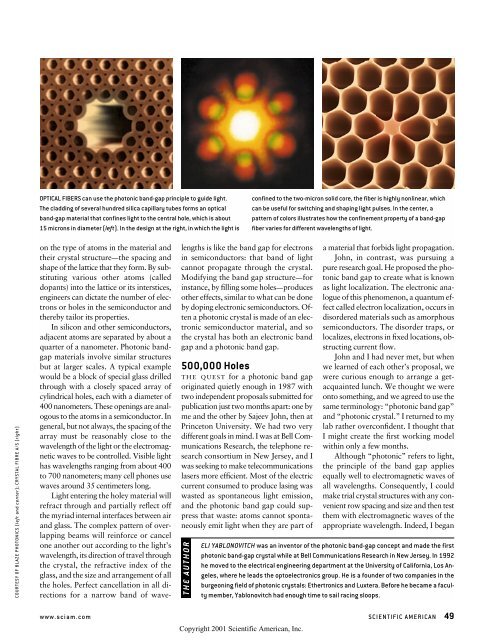
OPTICAL FIBERS can use the photonic band-gap principle to guide light.<br />
The cladding <strong>of</strong> several hundred silica capillary tubes forms an optical<br />
band-gap material that confines light to the central hole, which is about<br />
15 microns in diameter (left). In the design at the right, in which the light is<br />
confined to the two-micron solid core, the fiber is highly nonlinear, which<br />
can be useful for switching and shaping light pulses. In the center, a<br />
pattern <strong>of</strong> colors illustrates how the confinement property <strong>of</strong> a band-gap<br />
fiber varies for different wavelengths <strong>of</strong> light.<br />
COURTESY OF BLAZE PHOTONICS (left and center); CRYSTAL FIBRE A/S (right)<br />
on the type <strong>of</strong> atoms in the material and<br />
their crystal structure—the spacing and<br />
shape <strong>of</strong> the lattice that they form. By substituting<br />
various other atoms (called<br />
dopants) into the lattice or its interstices,<br />
engineers can dictate the number <strong>of</strong> electrons<br />
or holes in the semiconductor and<br />
thereby tailor its properties.<br />
In silicon and other semiconductors,<br />
adjacent atoms are separated by about a<br />
quarter <strong>of</strong> a nanometer. <strong>Photonic</strong> bandgap<br />
materials involve similar structures<br />
but at larger scales. A typical example<br />
would be a block <strong>of</strong> special glass drilled<br />
through with a closely spaced array <strong>of</strong><br />
cylindrical holes, each with a diameter <strong>of</strong><br />
400 nanometers. These openings are analogous<br />
to the atoms in a semiconductor. In<br />
general, but not always, the spacing <strong>of</strong> the<br />
array must be reasonably close to the<br />
wavelength <strong>of</strong> the light or the electromagnetic<br />
waves to be controlled. Visible light<br />
has wavelengths ranging from about 400<br />
to 700 nanometers; many cell phones use<br />
waves around 35 centimeters long.<br />
<strong>Light</strong> entering the holey material will<br />
refract through and partially reflect <strong>of</strong>f<br />
the myriad internal interfaces between air<br />
and glass. The complex pattern <strong>of</strong> overlapping<br />
beams will reinforce or cancel<br />
one another out according to the light’s<br />
wavelength, its direction <strong>of</strong> travel through<br />
the crystal, the refractive index <strong>of</strong> the<br />
glass, and the size and arrangement <strong>of</strong> all<br />
the holes. Perfect cancellation in all directions<br />
for a narrow band <strong>of</strong> wavelengths<br />
is like the band gap for electrons<br />
in semiconductors: that band <strong>of</strong> light<br />
cannot propagate through the crystal.<br />
Modifying the band gap structure—for<br />
instance, by filling some holes—produces<br />
other effects, similar to what can be done<br />
by doping electronic semiconductors. Often<br />
a photonic crystal is made <strong>of</strong> an electronic<br />
semiconductor material, and so<br />
the crystal has both an electronic band<br />
gap and a photonic band gap.<br />
500,000 Holes<br />
THE QUEST for a photonic band gap<br />
originated quietly enough in 1987 with<br />
two independent proposals submitted for<br />
publication just two months apart: one by<br />
me and the other by Sajeev John, then at<br />
Princeton University. We had two very<br />
different goals in mind. I was at Bell Communications<br />
<strong>Research</strong>, the telephone research<br />
consortium in New Jersey, and I<br />
was seeking to make telecommunications<br />
lasers more efficient. Most <strong>of</strong> the electric<br />
current consumed to produce lasing was<br />
wasted as spontaneous light emission,<br />
and the photonic band gap could suppress<br />
that waste: atoms cannot spontaneously<br />
emit light when they are part <strong>of</strong><br />
THE AUTHOR<br />
a material that forbids light propagation.<br />
John, in contrast, was pursuing a<br />
pure research goal. He proposed the photonic<br />
band gap to create what is known<br />
as light localization. The electronic analogue<br />
<strong>of</strong> this phenomenon, a quantum effect<br />
called electron localization, occurs in<br />
disordered materials such as amorphous<br />
semiconductors. The disorder traps, or<br />
localizes, electrons in fixed locations, obstructing<br />
current flow.<br />
John and I had never met, but when<br />
we learned <strong>of</strong> each other’s proposal, we<br />
were curious enough to arrange a getacquainted<br />
lunch. We thought we were<br />
onto something, and we agreed to use the<br />
same terminology: “photonic band gap”<br />
and “photonic crystal.” I returned to my<br />
lab rather overconfident. I thought that<br />
I might create the first working model<br />
within only a few months.<br />
Although “photonic” refers to light,<br />
the principle <strong>of</strong> the band gap applies<br />
equally well to electromagnetic waves <strong>of</strong><br />
all wavelengths. Consequently, I could<br />
make trial crystal structures with any convenient<br />
row spacing and size and then test<br />
them with electromagnetic waves <strong>of</strong> the<br />
appropriate wavelength. Indeed, I began<br />
ELI YABLONOVITCH was an inventor <strong>of</strong> the photonic band-gap concept and made the first<br />
photonic band-gap crystal while at Bell Communications <strong>Research</strong> in New Jersey. In 1992<br />
he moved to the electrical engineering department at the University <strong>of</strong> California, Los Angeles,<br />
where he leads the optoelectronics group. He is a founder <strong>of</strong> two companies in the<br />
burgeoning field <strong>of</strong> photonic crystals: Ethertronics and Luxtera. Before he became a faculty<br />
member, <strong>Yablonovitch</strong> had enough time to sail racing sloops.<br />
www.sciam.com SCIENTIFIC AMERICAN 49<br />
Copyright 2001 Scientific American, Inc.