Photonic Crystals: Semiconductors of Light - Yablonovitch Research ...
Photonic Crystals: Semiconductors of Light - Yablonovitch Research ...
Photonic Crystals: Semiconductors of Light - Yablonovitch Research ...

Create successful ePaper yourself
Turn your PDF publications into a flip-book with our unique Google optimized e-Paper software.
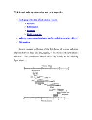
index as small as 1.87, and many optical<br />
materials are available with refractive indices<br />
as high as 3.6.<br />
The diamond structure isn’t the only<br />
structure having a photonic band gap. In<br />
1992 theorist Joseph W. Haus, then at<br />
Rensselaer Polytechnic Institute, showed<br />
that we had discarded the fcc structures<br />
too quickly. Scientists had searched the<br />
fcc structures for band gaps only at wavelengths<br />
for which about half a wave fits<br />
Butterflies and Microchips<br />
WE HAVE NOW LEARNED that nature<br />
already makes photonic crystals in the<br />
sparkling gem opal, in a butterfly’s colorful<br />
wings and in the hairs <strong>of</strong> a wormlike<br />
creature called the sea mouse. Each<br />
<strong>of</strong> these has a photonic band structure,<br />
though not a full band gap, in that light<br />
can still propagate in some directions. A<br />
complete band gap has eluded nature,<br />
perhaps because it requires too much refractive-index<br />
contrast.<br />
Nevertheless, an incomplete band<br />
gap can be very useful. For example, titanium<br />
dioxide particles smaller than a<br />
core, which confines light by total internal<br />
reflection. Philip St. J. Russell <strong>of</strong> the<br />
University <strong>of</strong> Bath in England demonstrated<br />
in 1999 how to make photonic<br />
band-gap fibers. In one version, light<br />
travels along a central hole in the fiber,<br />
confined there by the two-dimensional<br />
band gap <strong>of</strong> the surrounding material.<br />
More optical power can be sent through<br />
such a central void than through glass,<br />
enabling greater information-carrying<br />
Integrated circuits that combine<br />
conventional electronics and photonic crystals would represent<br />
the ultimate limit <strong>of</strong> optoelectronic miniaturization.<br />
in one cell <strong>of</strong> the lattice (somewhat like<br />
the fundamental vibration <strong>of</strong> a guitar<br />
string). As we saw, only a pseudo-gap occurs<br />
at that frequency. Haus, however,<br />
also considered a higher frequency, for<br />
which a full wavelength fits in a cell<br />
(somewhat like the first harmonic <strong>of</strong> the<br />
guitar string), and proved that an fcc<br />
band gap would indeed emerge there. In<br />
addition, he discovered that even the simple<br />
cubic configuration known as the<br />
scaffold structure (for its similarity to<br />
scaffolding) could have a band gap, albeit<br />
a small one.<br />
micron can be made to self-assemble in<br />
the opal structure. Titanium dioxide is<br />
the intensely white pigment used in paint<br />
and to make paper white. The coherent<br />
scattering <strong>of</strong> light that occurs from bandgap-structured<br />
titanium dioxide can impart<br />
more whiteness for less mass <strong>of</strong> titanium<br />
dioxide. One day photonic crystals<br />
may be all around us in the painted<br />
walls and in the stacks <strong>of</strong> paper cluttering<br />
our desks.<br />
Another very useful type <strong>of</strong> incomplete<br />
band gap material is that <strong>of</strong> two-dimensional<br />
photonic crystals, which can<br />
block light from traveling within a plane.<br />
Such a structure can be stretched along<br />
the third dimension, forming a new kind<br />
<strong>of</strong> optical fiber. Conventional optical<br />
fibers have a high refractive index at their<br />
APPLICATIONS FORPHOTONICCRYSTALS<br />
DEVICE<br />
OPTICAL FIBERS<br />
DESCRIPTION<br />
2-D band-gap material stretched along the third dimension<br />
capacity, perhaps 100 times that <strong>of</strong> conventional<br />
telecommunications fibers.<br />
Specialty fibers have advanced the most<br />
as commercial photonic band-gap products.<br />
Companies in Denmark and the<br />
U.K. have already distributed sample<br />
quantities and will soon begin volume<br />
production.<br />
Instead <strong>of</strong> stretching out a two-dimensional<br />
band-gap structure to make a<br />
fiber, one can go to the other extreme and<br />
make a two-dimensional thin-film photonic<br />
crystal, as was first calculated in<br />
1997 by Shanhui Fan and John D.<br />
Joannopoulos, then both at the Massachusetts<br />
Institute <strong>of</strong> Technology. Thinfilm<br />
photonic crystals can be easily patterned<br />
by standard methods used to produce<br />
integrated circuits. Introducing<br />
STATUS<br />
Early versions already commercialized<br />
NANOSCOPIC LASERS<br />
ULTRAWHITE PIGMENT<br />
RADIO-FREQUENCY<br />
ANTENNAS, REFLECTORS<br />
LIGHT-EMITTING DIODES<br />
PHOTONIC INTEGRATED<br />
CIRCUITS<br />
World’s tiniest optical cavities and tiniest lasers;<br />
formed in a thin-film 2-D band-gap material<br />
Incomplete 3-D band-gap material, usually patterned<br />
as opal structure<br />
Uses inductors and capacitors in place <strong>of</strong> ordinary<br />
dielectric materials<br />
<strong>Photonic</strong> band-gap structure can extract light very efficiently<br />
(better than 50%)<br />
2-D thin films can be patterned like conventional integrated<br />
circuits to make channel filters, modulators, couplers and so on<br />
Demonstrated in the lab<br />
Demonstrated; low-cost manufacturing<br />
methods under development<br />
Demonstrated for magnetic resonance<br />
imaging and antennas<br />
Demonstrated, but must compete with<br />
other methods <strong>of</strong> achieving the same goal<br />
Under development<br />
54 SCIENTIFIC AMERICAN DECEMBER 2001<br />
Copyright 2001 Scientific American, Inc.