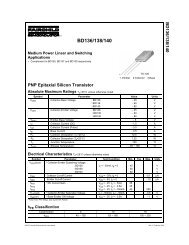
Application Note 116 Use the LM158/LM258/LM358 Dual, Single ...
Application Note 116 Use the LM158/LM258/LM358 Dual, Single ...
Application Note 116 Use the LM158/LM258/LM358 Dual, Single ...

Create successful ePaper yourself
Turn your PDF publications into a flip-book with our unique Google optimized e-Paper software.
<strong>Use</strong> <strong>the</strong><br />
<strong>LM158</strong>/<strong>LM258</strong>/<strong>LM358</strong> <strong>Dual</strong>,<br />
<strong>Single</strong> Supply Op Amp<br />
Introduction<br />
<strong>Use</strong> <strong>the</strong> <strong>LM158</strong>/<strong>LM258</strong>/<strong>LM358</strong> dual op amp with a single<br />
supply in place of <strong>the</strong> LM1458/LM1558 with split supply and<br />
reap <strong>the</strong> profits in terms of:<br />
a. Input and output voltage range down to <strong>the</strong> negative<br />
(ground) rail<br />
b. <strong>Single</strong> supply operation<br />
c. Lower standby power dissipation<br />
d. Higher output voltage swing<br />
e. Lower input offset current<br />
f. Generally similar performance o<strong>the</strong>rwise<br />
The main advantage, of course, is that you can eliminate <strong>the</strong><br />
negative supply in many applications and still retain equivalent<br />
op amp performance. Additionally, and in some cases<br />
more importantly, <strong>the</strong> input and output levels are permitted to<br />
swing down to ground (negative rail) potential. Table 1<br />
shows <strong>the</strong> relative performance of <strong>the</strong> two in terms of guaranteed<br />
and/or typical specifications.<br />
National Semiconductor<br />
<strong>Application</strong> <strong>Note</strong> <strong>116</strong><br />
August 1980<br />
In many applications <strong>the</strong> <strong>LM158</strong>/<strong>LM258</strong>/<strong>LM358</strong> can also be<br />
used directly in place of LM1558 for split supply operation.<br />
<strong>Single</strong> Supply Operation<br />
The LM1458/LM1558 or similar op amps exhibit several<br />
important limitations when operated from a single positive<br />
(or negative) supply. Chief among <strong>the</strong>se is that input and<br />
output signal swing is severely limited for a given supply as<br />
shown in Figure 1. For linear operation, <strong>the</strong> input voltage<br />
must not reach within 3 volts of ground or of <strong>the</strong> supply, and<br />
output range is similarly limited to within 3–5 volts of ground<br />
or supply. This means that operation with a +12V supply<br />
could be limited as low as 2 Vp-p output swing. The <strong>LM358</strong><br />
however, allows a 10.5 Vp-p output swing for <strong>the</strong> same 12V<br />
supply. Admittedly <strong>the</strong>se are worst case specification limits,<br />
but <strong>the</strong>y serve to illustrate <strong>the</strong> problem.<br />
TABLE 1. Comparison of <strong>Dual</strong> Op Amps LM1458 and <strong>LM358</strong><br />
Characteristic LM1458 <strong>LM358</strong><br />
V IO 6mVMax 7mVMax<br />
CM V I 24 Vp-p* 0–28.5V*<br />
I IO 200 nA 50 nA<br />
I OB 500 nA −500 nA<br />
CMRR<br />
60 dB Min @ 100 Hz<br />
85 dB Typ @ DC<br />
90 dB Typ<br />
e n @ 1 kHz, R GEN 10 kΩ 45 nV/√Hz Typ 40 nV/√Hz Typ**<br />
Z IN 200 MΩ Typ Typ 100 MΩ<br />
A VOL<br />
20k Min<br />
100k Typ<br />
100k Typ<br />
f c 1.1 MHz Typ 1 MHz Typ **<br />
P BW 14 kHz Typ 11 kHz Typ **<br />
dV o /dt 0.8V/µs Typ 0.5V/µs Typ**<br />
V o @ R L = 10k/2k 24/20 Vp-p* 28.5 Vp-p<br />
I SC 20 mA Typ Source 20 mA Min (40 Typ)<br />
Sink 10 mA Min (20 Typ)<br />
PSRR @ DC<br />
37 dB Min<br />
100 dB Typ<br />
90 dB Typ<br />
I D (R L = ∞) 8 mA Max 2 mA Max<br />
‡From laboratory measurement<br />
*Based on V S = 30V on <strong>LM358</strong> only, or V S = ±15V<br />
**From data sheet typical curves<br />
<strong>Use</strong> <strong>the</strong> <strong>LM158</strong>/<strong>LM258</strong>/<strong>LM358</strong> <strong>Dual</strong>, <strong>Single</strong> Supply Op Amp AN-<strong>116</strong><br />
© 2002 National Semiconductor Corporation AN007424 www.national.com
AN-<strong>116</strong><br />
<strong>Single</strong> Supply Operation (Continued)<br />
00742401 00742402<br />
FIGURE 1. Worst Case Signal Levels with +12V Supply<br />
00742403 00742404<br />
FIGURE 2. Operating with AC Signals<br />
AC Gain<br />
For AC signals <strong>the</strong> input can be capacitor coupled. The input<br />
common mode and quiescent output voltages are fixed at<br />
one-half <strong>the</strong> supply voltage by a resistive divider at <strong>the</strong><br />
non-inverting input as shown in Figure 2. This quiescent<br />
output could be set at a lower voltage to minimize power<br />
dissipation in <strong>the</strong> <strong>LM358</strong>, if desired, so long as V Q ≥ V IN pk.<br />
For <strong>the</strong> LM1458 <strong>the</strong> quiescent output must be higher, VQ ≥<br />
3V+V IN pk thus, for small signals, power dissipation is much<br />
greater with <strong>the</strong> LM1458. Example: Required V O =V Q<br />
±1V<br />
pk into 2k, V SUPPLY = as required. Find quiescent dissipation<br />
in load and amplifier for LM1458 and <strong>LM358</strong>.<br />
The LM1458 requires over twice <strong>the</strong> supply voltage and<br />
nearly 10 times <strong>the</strong> supply power of <strong>the</strong> <strong>LM358</strong> in this<br />
application.<br />
Inverting DC Gain<br />
Connections and biasing for DC inverting gain are essentially<br />
<strong>the</strong> same as for <strong>the</strong> AC coupled case. <strong>Note</strong>, of course,<br />
that <strong>the</strong> output cannot swing negative when operated from a<br />
single positive supply. Figure 3 shows <strong>the</strong> connections and<br />
signal limitations.<br />
www.national.com 2
Non-Inverting DC Gain<br />
The non-inverting gain connection does not require <strong>the</strong> V Q<br />
biasing as before; <strong>the</strong> inverting input can be returned to<br />
ground in <strong>the</strong> usual manner for gains greater than unity, (see<br />
Figure 4). A tremendous advantage of <strong>the</strong> <strong>LM358</strong> in this<br />
connection is that input signals and output may extend all <strong>the</strong><br />
way to ground; <strong>the</strong>refore DC signals in <strong>the</strong> low-millivolt range<br />
can be handled. The LM1458 still requires that V IN =<br />
3V–17V. Therefore maximum gain is limited to A V =(V O −3)/<br />
3, or A V max = 5.4 for a 20V supply.<br />
There is no similar limitation for <strong>the</strong> <strong>LM358</strong>.<br />
Zero T.C. Input Bias Current<br />
An interesting and unusual characteristic is that I IN has a<br />
zero temperature coefficient. This means that matched resistance<br />
is not required at <strong>the</strong> input, allowing omission of one<br />
resistor per op amp from <strong>the</strong> circuit in most cases.<br />
Balanced Supply Operation<br />
The <strong>LM358</strong> will operate satisfactorily in balanced supply<br />
operation so long as a load is maintained from output to <strong>the</strong><br />
negative supply.<br />
AN-<strong>116</strong><br />
00742405 00742406<br />
FIGURE 3. Typical DC Coupled Inverting Gain<br />
00742407 00742408<br />
FIGURE 4. Typical DC Coupled Non-Inverting Gain<br />
00742409<br />
FIGURE 5. Split Supply Operation of <strong>LM358</strong><br />
The output load to negative supply forces <strong>the</strong> amplifier to<br />
source some minimum current at all times, thus eliminating<br />
crossover distortion. Crossover distortion without this load<br />
would be more severe than that expected with <strong>the</strong> normal op<br />
amp. Since <strong>the</strong> single supply design took notice of this<br />
normal load connection to ground, a class AB output stage<br />
3<br />
www.national.com
AN-<strong>116</strong> <strong>Use</strong> <strong>the</strong> <strong>LM158</strong>/<strong>LM258</strong>/<strong>LM358</strong> <strong>Dual</strong>, <strong>Single</strong> Supply Op Amp<br />
Balanced Supply Operation<br />
(Continued)<br />
was not included. Where ground referenced feedback resistors<br />
are used as in Figure 5, <strong>the</strong> required load to <strong>the</strong> negative<br />
supply depends upon <strong>the</strong> peak negative output signal level<br />
desired without exhibiting crossover distortion. R L to <strong>the</strong><br />
negative rail should be chosen small enough that <strong>the</strong> voltage<br />
divider formed by R F and R L will permit V o to swing negative<br />
to <strong>the</strong> desired point according to <strong>the</strong> equation:<br />
R L could also be returned to <strong>the</strong> positive supply with <strong>the</strong><br />
advantage that V o max would never exceed (V S<br />
+ − 1.5V).<br />
Then with ±15V supplies R L MIN would be 0.12 R F . The<br />
disadvantage would be that <strong>the</strong> <strong>LM358</strong> can source twice as<br />
much current as it can sink, <strong>the</strong>refore R L to negative supply<br />
can be one-half <strong>the</strong> value of R L to positive supply.<br />
The need for single or split supply is based on system<br />
requirements which may be o<strong>the</strong>r than op amp oriented.<br />
However if <strong>the</strong> only need for balanced supplies is to simplify<br />
<strong>the</strong> biasing of op amps, <strong>the</strong>re are many systems which can<br />
find a cost effective benefit in operating <strong>LM358</strong>’s from single<br />
supplies ra<strong>the</strong>r than standard op amps from balanced supplies.<br />
Of <strong>the</strong> usual op amp circuits, Table 2 shows those few<br />
which have limited function with single supply operation.<br />
Most are based on <strong>the</strong> premise that to operate from a single<br />
supply, a reference V Q at about one-half <strong>the</strong> supply be<br />
available for bias or (zero) signal reference. The basic circuits<br />
are those listed in AN-20.<br />
LIFE SUPPORT POLICY<br />
TABLE 2. Conventional Op Amp Circuits<br />
Suitable for <strong>Single</strong> Supply Operation<br />
<strong>Application</strong><br />
Limitations<br />
AC Coupled amp‡ V Q *<br />
Inverting amp<br />
V Q<br />
Non-inverting amp<br />
OK*<br />
Unity gain buffer<br />
OK<br />
Summing amp<br />
V Q<br />
Difference amp<br />
V Q<br />
Differentiator<br />
V Q<br />
Integrator<br />
V Q<br />
LP Filter<br />
V Q<br />
I–V Connector<br />
V Q<br />
PE Cell Amp<br />
OK<br />
I Source<br />
I Sink<br />
OK<br />
Volt Ref<br />
OK<br />
FW Rectifier<br />
V Q or modified circuit<br />
Sine wave osc<br />
V Q<br />
Triangular generator V Q<br />
Threshold detector<br />
OK<br />
Tracking, regulator PS Not practical<br />
Programmable PS<br />
OK<br />
Peak Detector OK to V IN =0<br />
‡See AN-20 for conventional circuits<br />
*V Q denotes need for a reference voltage, usually at about<br />
OK means no reference voltage required<br />
NATIONAL’S PRODUCTS ARE NOT AUTHORIZED FOR USE AS CRITICAL COMPONENTS IN LIFE SUPPORT<br />
DEVICES OR SYSTEMS WITHOUT THE EXPRESS WRITTEN APPROVAL OF THE PRESIDENT AND GENERAL<br />
COUNSEL OF NATIONAL SEMICONDUCTOR CORPORATION. As used herein:<br />
1. Life support devices or systems are devices or<br />
systems which, (a) are intended for surgical implant<br />
into <strong>the</strong> body, or (b) support or sustain life, and<br />
whose failure to perform when properly used in<br />
accordance with instructions for use provided in <strong>the</strong><br />
labeling, can be reasonably expected to result in a<br />
significant injury to <strong>the</strong> user.<br />
National Semiconductor<br />
Corporation<br />
Americas<br />
Email: support@nsc.com<br />
www.national.com<br />
National Semiconductor<br />
Europe<br />
Fax: +49 (0) 180-530 85 86<br />
Email: europe.support@nsc.com<br />
Deutsch Tel: +49 (0) 69 9508 6208<br />
English Tel: +44 (0) 870 24 0 2171<br />
Français Tel: +33 (0) 1 41 91 8790<br />
2. A critical component is any component of a life<br />
support device or system whose failure to perform<br />
can be reasonably expected to cause <strong>the</strong> failure of<br />
<strong>the</strong> life support device or system, or to affect its<br />
safety or effectiveness.<br />
National Semiconductor<br />
Asia Pacific Customer<br />
Response Group<br />
Tel: 65-2544466<br />
Fax: 65-2504466<br />
Email: ap.support@nsc.com<br />
National Semiconductor<br />
Japan Ltd.<br />
Tel: 81-3-5639-7560<br />
Fax: 81-3-5639-7507<br />
National does not assume any responsibility for use of any circuitry described, no circuit patent licenses are implied and National reserves <strong>the</strong> right at any time without notice to change said circuitry and specifications.