
You also want an ePaper? Increase the reach of your titles
YUMPU automatically turns print PDFs into web optimized ePapers that Google loves.
<strong>TC4426</strong><br />
TC4427<br />
TC4428<br />
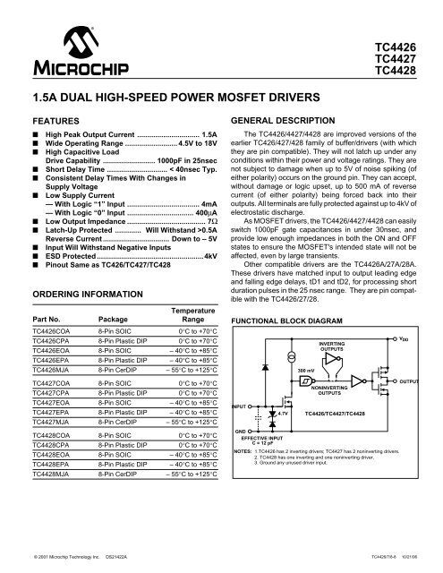
1.5A DUAL HIGH-SPEED POWER <strong>MOSFET</strong> DRIVERS<br />
FEATURES<br />
■ High Peak Output Current ............................... 1.5A<br />
■ Wide Operating Range .......................... 4.5V to 18V<br />
■ High Capacitive Load<br />
Drive Capability .......................... 1000pF in 25nsec<br />
■ Short Delay Time .............................. < 40nsec Typ.<br />
■ Consistent Delay Times With Changes in<br />
Supply Voltage<br />
■ Low Supply Current<br />
— With Logic “1” Input .................................... 4mA<br />
— With Logic “0” Input ................................. 400µA<br />
■ Low Output Impedance ....................................... 7Ω<br />
■ Latch-Up Protected ............. Will Withstand >0.5A<br />
Reverse Current ................................. Down to – 5V<br />
■ Input Will Withstand Negative Inputs<br />
■ ESD Protected .....................................................4kV<br />
■ Pinout Same as TC426/TC427/TC428<br />
ORDERING INFORMATION<br />
Temperature<br />
Part No. Package Range<br />
<strong>TC4426</strong>COA 8-Pin SOIC 0°C to +70°C<br />
<strong>TC4426</strong>CPA 8-Pin Plastic DIP 0°C to +70°C<br />
<strong>TC4426</strong>EOA 8-Pin SOIC – 40°C to +85°C<br />
<strong>TC4426</strong>EPA 8-Pin Plastic DIP – 40°C to +85°C<br />
<strong>TC4426</strong>MJA 8-Pin CerDIP – 55°C to +125°C<br />
TC4427COA 8-Pin SOIC 0°C to +70°C<br />
TC4427CPA 8-Pin Plastic DIP 0°C to +70°C<br />
TC4427EOA 8-Pin SOIC – 40°C to +85°C<br />
TC4427EPA 8-Pin Plastic DIP – 40°C to +85°C<br />
TC4427MJA 8-Pin CerDIP – 55°C to +125°C<br />
TC4428COA 8-Pin SOIC 0°C to +70°C<br />
TC4428CPA 8-Pin Plastic DIP 0°C to +70°C<br />
TC4428EOA 8-Pin SOIC – 40°C to +85°C<br />
TC4428EPA 8-Pin Plastic DIP – 40°C to +85°C<br />
TC4428MJA 8-Pin CerDIP – 55°C to +125°C<br />
GENERAL DESCRIPTION<br />
The <strong>TC4426</strong>/4427/4428 are improved versions of the<br />
earlier TC426/427/428 family of buffer/drivers (with which<br />
they are pin compatible). They will not latch up under any<br />
conditions within their power and voltage ratings. They are<br />
not subject to damage when up to 5V of noise spiking (of<br />
either polarity) occurs on the ground pin. They can accept,<br />
without damage or logic upset, up to 500 mA of reverse<br />
current (of either polarity) being forced back into their<br />
outputs. All terminals are fully protected against up to 4kV of<br />
electrostatic discharge.<br />
As <strong>MOSFET</strong> drivers, the <strong>TC4426</strong>/4427/4428 can easily<br />
switch 1000pF gate capacitances in under 30nsec, and<br />
provide low enough impedances in both the ON and OFF<br />
states to ensure the <strong>MOSFET</strong>'s intended state will not be<br />
affected, even by large transients.<br />
Other compatible drivers are the <strong>TC4426</strong>A/27A/28A.<br />
These drivers have matched input to output leading edge<br />
and falling edge delays, tD1 and tD2, for processing short<br />
duration pulses in the 25 nsec range. They are pin compatible<br />
with the <strong>TC4426</strong>/27/28.<br />
FUNCTIONAL BLOCK DIAGRAM<br />
INPUT<br />
4.7V<br />
300 mV<br />
INVERTING<br />
OUTPUTS<br />
NONINVERTING<br />
OUTPUTS<br />
<strong>TC4426</strong>/TC4427/TC4428<br />
GND<br />
EFFECTIVE INPUT<br />
C = 12 pF<br />
NOTES: 1.<strong>TC4426</strong> has 2 inverting drivers; TC4427 has 2 noninverting drivers.<br />
2. TC4428 has one inverting and one noninverting driver.<br />
3. Ground any unused driver input.<br />
V DD<br />
OUTPUT<br />
© 2001 Microchip Technology Inc. DS21422A<br />
<strong>TC4426</strong>/7/8-8 10/21/96
1.5A DUAL HIGH-SPEED POWER <strong>MOSFET</strong> DRIVERS<br />
<strong>TC4426</strong><br />
TC4427<br />
TC4428<br />
ABSOLUTE MAXIMUM RATINGS*<br />
Supply Voltage ......................................................... +22V<br />
Input Voltage, IN A or IN B . (V DD + 0.3V) to (GND – 5.0V)<br />
Maximum Chip Temperature................................. +150°C<br />
Storage Temperature Range ................ – 65°C to +150°C<br />
Lead Temperature (Soldering, 10 sec) ................. +300°C<br />
Package Thermal Resistance<br />
CerDIP R θJ-A ................................................ 150°C/W<br />
CerDIP R θJ-C .................................................. 50°C/W<br />
PDIP R θJ-A ................................................... 125°C/W<br />
PDIP R θJ-C ..................................................... 42°C/W<br />
SOIC R θJ-A ................................................... 155°C/W<br />
SOIC R θJ-C ..................................................... 45°C/W<br />
PIN CONFIGURATIONS<br />
Operating Temperature Range<br />
C Version ............................................... 0°C to +70°C<br />
E Version .......................................... – 40°C to +85°C<br />
M Version ....................................... – 55°C to +125°C<br />
Package Power Dissipation (T A ≤ 70°C)<br />
Plastic .............................................................730mW<br />
CerDIP ............................................................800mW<br />
SOIC ...............................................................470mW<br />
*Static-sensitive device. Unused devices must be stored in conductive<br />
material. Protect devices from static discharge and static fields. Stresses<br />
above those listed under "Absolute Maximum Ratings" may cause permanent<br />
damage to the device. These are stress ratings only and functional<br />
operation of the device at these or any other conditions above those<br />
indicated in the operation sections of the specifications is not implied.<br />
Exposure to absolute maximum rating conditions for extended periods may<br />
affect device reliability.<br />
NC<br />
1<br />
8<br />
NC<br />
NC<br />
1<br />
8<br />
NC<br />
NC<br />
1<br />
8<br />
NC<br />
IN A<br />
GND<br />
2<br />
3<br />
<strong>TC4426</strong><br />
7<br />
6<br />
OUT A<br />
V DD<br />
IN A<br />
GND<br />
2<br />
3<br />
TC4427<br />
7<br />
6<br />
OUT A<br />
V DD<br />
IN A<br />
GND<br />
2<br />
3<br />
TC4428<br />
7<br />
6<br />
OUT A<br />
V DD<br />
IN B<br />
4<br />
5<br />
OUT B<br />
IN B<br />
4<br />
5<br />
OUT B<br />
IN B<br />
4<br />
5<br />
OUT B<br />
2<br />
7<br />
2,4 7,5<br />
2,4 7,5<br />
4<br />
5<br />
INVERTING<br />
NC = NO INTERNAL CONNECTION<br />
NOTE: SOIC pinout is identical to DIP.<br />
NONINVERTING<br />
DIFFERENTIAL<br />
ELECTRICAL CHARACTERISTICS: T A = +25°C with 4.5V ≤ V DD ≤ 18V, unless otherwise specified.<br />
Symbol Parameter Test Conditions Min Typ Max Unit<br />
Input<br />
V IH Logic 1 High Input Voltage 2.4 — — V<br />
V IL Logic 0 Low Input Voltage — — 0.8 V<br />
I IN Input Current 0V ≤ V IN ≤ V DD – 1 — 1 µA<br />
Output<br />
V OH High Output Voltage V DD – 0.025 — — V<br />
V OL Low Output Voltage — — 0.025 V<br />
R O Output Resistance V DD = 18V, I O = 10mA — 7 10 Ω<br />
I PK Peak Output Current Duty Cycle ≤ 2%, t ≤ 30µsec — 1.5 — A<br />
I REV Latch-Up Protection Duty Cycle ≤ 2% > 0.5 — — A<br />
Withstand Reverse Current t ≤ 30 µsec<br />
Switching Time (Note 1)<br />
t R Rise Time Figure 1 — 19 30 nsec<br />
t F Fall Time Figure 1 — 19 30 nsec<br />
t D1 Delay Time Figure 1 — 20 30 nsec<br />
t D2 Delay Time Figure 1 — 40 50 nsec<br />
Power Supply<br />
I S Power Supply Current V IN = 3V (Both Inputs) — — 4.5 mA<br />
V IN = 0V (Both Inputs) — — 0.4 mA<br />
NOTE: 1. Switching times are guaranteed by design.<br />
<strong>TC4426</strong>/7/8-8 10/21/96<br />
2<br />
© 2001 Microchip Technology Inc. DS21422A
1.5A DUAL HIGH-SPEED POWER <strong>MOSFET</strong> DRIVERS<br />
<strong>TC4426</strong><br />
TC4427<br />
TC4428<br />
ELECTRICAL CHARACTERISTICS: Specifications measured over operating temperature range with 4.5V ≤<br />
V DD ≤ 18V, unless otherwise specified.<br />
Symbol Parameter Test Conditions Min Typ Max Unit<br />
Input<br />
V IH Logic 1 High Input Voltage 2.4 — — V<br />
V IL Logic 0 Low Input Voltage — — 0.8 V<br />
I IN Input Current 0V ≤ V IN ≤ V DD – 10 — 10 µA<br />
Output<br />
V OH High Output Voltage V DD – 0.025 — — V<br />
V OL Low Output Voltage — — 0.025 V<br />
R O Output Resistance V DD = 18V, I O = 10mA — 9 12 Ω<br />
I PK Peak Output Current Duty Cycle ≤ 2%, t ≤ 300µsec — 1.5 — A<br />
I REV Latch-Up Protection Duty Cycle≤ 2% > 0.5 — — A<br />
Withstand Reverse Current<br />
t ≤ 300µsec<br />
Switching Time (Note 1)<br />
t R Rise Time Figure 1 — — 40 nsec<br />
t F Fall Time Figure 1 — — 40 nsec<br />
t D1 Delay Time Figure 1 — — 40 nsec<br />
t D2 Delay Time Figure 1 — — 60 nsec<br />
Power Supply<br />
I S Power Supply Current V IN = 3V (Both Inputs) — — 8 mA<br />
V IN = 0V (Both Inputs) — — 0.6 mA<br />
NOTE: 1. Switching times are guaranteed by design.<br />
A • sec<br />
10 –8<br />
9<br />
8<br />
7<br />
6<br />
5<br />
4<br />
3<br />
2<br />
Crossover Energy Loss<br />
INPUT<br />
V DD = 18V<br />
4.7 µF<br />
6<br />
2,4 5,7<br />
0.1 µF<br />
OUTPUT<br />
C L = 1000 pF<br />
+5V<br />
INPUT<br />
0V<br />
V DD<br />
OUTPUT<br />
0V<br />
10%<br />
90%<br />
t D1 t F<br />
t D2<br />
t R<br />
90%<br />
90%<br />
10%<br />
10%<br />
Inverting <strong>Driver</strong><br />
10 –9<br />
4<br />
6 8 10 12 14 16<br />
V DD<br />
18<br />
3<br />
+5V<br />
INPUT<br />
0V<br />
10%<br />
90%<br />
MAX. POWER (mW)<br />
1600<br />
1400<br />
1200<br />
1000<br />
800<br />
600<br />
400<br />
8 Pin DIP<br />
8 Pin CerDIP<br />
8 Pin SOIC<br />
Thermal Derating Curves<br />
200<br />
0<br />
0 10 20 30 40 50 60 70 80 90 100 110 120<br />
AMBIENT TEMPERATURE (°C)<br />
INPUT: 100 kHz, square wave,<br />
t RISE = t FALL ≤ 10ns<br />
V DD<br />
OUTPUT<br />
0V<br />
90%<br />
t D1<br />
Figure 1. Switching Time Test Circuit<br />
t R<br />
90%<br />
tD2<br />
10% 10%<br />
Noninverting <strong>Driver</strong><br />
NOTE: The values on this graph represent the loss seen by both drivers in a package<br />
during one complete cycle. For a single driver, divide the stated values by 2. For a<br />
single transition of a single driver, divide the stated value by 4.<br />
t F<br />
3<br />
© 2001 Microchip Technology Inc. DS21422A <strong>TC4426</strong>/7/8-8 10/21/96
1.5A DUAL HIGH-SPEED POWER <strong>MOSFET</strong> DRIVERS<br />
<strong>TC4426</strong><br />
TC4427<br />
TC4428<br />
TYPICAL CHARACTERISTICS<br />
t RISE (nsec)<br />
100<br />
80<br />
60<br />
40<br />
Rise Time vs. Supply Voltage<br />
Fall Time vs. Supply Voltage<br />
100<br />
2200 pF T A = 25°C<br />
2200 pF<br />
T A = 25°C<br />
1500 pF<br />
1000 pF<br />
470 pF<br />
t FALL (nsec)<br />
80<br />
1500 pF<br />
60<br />
1000 pF<br />
40<br />
470 pF<br />
20<br />
100 pF<br />
20<br />
100 pF<br />
0<br />
4 6 8 10 12 14 16 18<br />
V DD<br />
0<br />
4 6 8 10 12 14 16 18<br />
V DD<br />
100<br />
80<br />
Rise TIme vs. Capacitive Load<br />
Fall TIme vs. Capacitive Load<br />
100<br />
5V<br />
T<br />
5V<br />
A = 25°C T A = 25°C<br />
80<br />
t RISE (nsec)<br />
60<br />
40<br />
10V<br />
15V<br />
t FALL (nsec)<br />
60<br />
40<br />
10V<br />
15V<br />
20<br />
20<br />
0<br />
100 1000 10,000<br />
C LOAD (pF)<br />
0<br />
100 1000 10,000<br />
C LOAD (pF)<br />
60<br />
50<br />
Rise and Fall Times vs. Temperature<br />
C LOAD = 1000 pF<br />
V DD = 17.5V<br />
60<br />
50<br />
Propagation Delay vs. Supply Voltage<br />
C LOAD = 1000 pF<br />
t D2<br />
TIME (nsec)<br />
40<br />
30<br />
t FALL<br />
DELAY TIME (nsec)<br />
40<br />
30<br />
t D1<br />
T A = 25°C<br />
20<br />
t RISE<br />
20<br />
<strong>TC4426</strong>/7/8-8 10/21/96<br />
10<br />
–55 –35 –15 5 25 45 65 85 105 125<br />
TEMPERATURE (°C)<br />
4<br />
10<br />
4 6 8 10 12 14 16 18<br />
V DD<br />
© 2001 Microchip Technology Inc. DS21422A
1.5A DUAL HIGH-SPEED POWER <strong>MOSFET</strong> DRIVERS<br />
<strong>TC4426</strong><br />
TC4427<br />
TC4428<br />
TYPICAL CHARACTERISTICS (Cont.)<br />
DELAY TIME (nsec)<br />
Effect of Input Amplitude on Delay Time<br />
60<br />
C LOAD = 1000 pF<br />
50<br />
V DD = 10V<br />
40<br />
t D2<br />
30<br />
DELAY TIME (nsec)<br />
Propagation Delay Time vs. Temperature<br />
60<br />
V DD = 18V<br />
V LOAD= 1000 pF<br />
50<br />
t D2<br />
40<br />
t<br />
30<br />
D1<br />
20<br />
20<br />
10<br />
0 2 4 6 8 10<br />
V DRIVE (V)<br />
10<br />
–55 –35 –15 5 25 45 65 85 105 125<br />
T A (°C)<br />
Quiescent Supply Current vs. Voltage<br />
T = +25°C A<br />
I<br />
QUIESCENT<br />
(mA)<br />
1<br />
BOTH INPUTS = 1<br />
I QUIESCENT (mA)<br />
3.5<br />
3.0<br />
2.5<br />
BOTH INPUTS = 0<br />
0.1<br />
4<br />
t D1<br />
V DD<br />
Quiescent Supply Current vs. Temperature<br />
4.0<br />
V DD = 18V<br />
BOTH INPUTS = 1<br />
6 8 10 12 14 16<br />
18<br />
2.0<br />
–55 –35 –15 5 25 45 65 85 105 125<br />
T A (°C)<br />
25<br />
High-State Output Resistance<br />
25<br />
Low-State Output Resistance<br />
R DS(ON) (Ω)<br />
20<br />
15<br />
10<br />
WORST CASE @ T J = +150°C<br />
TYP @ T A = +25°C<br />
R DS(ON) (Ω)<br />
20<br />
15<br />
10<br />
WORST CASE @ T J = +150°C<br />
TYP @ T A = +25°C<br />
8<br />
8<br />
5<br />
5<br />
4 6 8 10 12 14 16 18 4 6 8 10 12 14 16 18<br />
V DD<br />
V DD<br />
5<br />
© 2001 Microchip Technology Inc. DS21422A <strong>TC4426</strong>/7/8-8 10/21/96
1.5A DUAL HIGH-SPEED POWER <strong>MOSFET</strong> DRIVERS<br />
<strong>TC4426</strong><br />
TC4427<br />
TC4428<br />
SUPPLY CURRENT CHARACTERISTICS (Load on Single Output Only)<br />
I SUPPLY (mA)<br />
60<br />
50<br />
40<br />
30<br />
20<br />
Supply Current vs. Capacitive Load<br />
2 MHz<br />
V DD = 18V<br />
900 kHz<br />
600 kHz<br />
I SUPPLY (mA)<br />
60<br />
50<br />
40<br />
30<br />
20<br />
Supply Current vs. Frequency<br />
1000 pF<br />
V DD = 18V<br />
2200 pF<br />
100 pF<br />
10<br />
200 kHz<br />
10<br />
20 kHz<br />
0<br />
100 1000 10,000<br />
C<br />
LOAD<br />
(pF)<br />
0<br />
10 100 1000<br />
FREQUENCY (kHz)<br />
60<br />
50<br />
Supply Current vs. Capacitive Load<br />
Supply Current vs. Frequency<br />
60<br />
2200 pF<br />
V DD = 12V<br />
2 MHz<br />
V DD = 12V<br />
50<br />
I SUPPLY (mA)<br />
40<br />
30<br />
20<br />
900 kHz<br />
600 kHz<br />
I SUPPLY (mA)<br />
40<br />
30<br />
20<br />
1000 pF<br />
100 pF<br />
10<br />
200 kHz<br />
0<br />
20 kHz<br />
100 1000 10,000<br />
C LOAD (pF)<br />
10<br />
0<br />
10 100 1000<br />
FREQUENCY (kHz)<br />
60<br />
50<br />
Supply Current vs. Capacitive Load<br />
Supply Current vs. Frequency<br />
60<br />
V DD = 6V<br />
V<br />
DD<br />
= 6V<br />
50<br />
I SUPPLY (mA)<br />
40<br />
30<br />
20<br />
2 MHz<br />
I SUPPLY (mA)<br />
40<br />
30<br />
20<br />
1000 pF<br />
2200 pF<br />
900 kHz<br />
10<br />
600 kHz<br />
200 kHz<br />
20 kHz<br />
0<br />
100 1000 10,000<br />
C<br />
LOAD<br />
(pF)<br />
<strong>TC4426</strong>/7/8-8 10/21/96<br />
6<br />
10<br />
0<br />
10 100 1000<br />
FREQUENCY (kHz)<br />
100 pF<br />
© 2001 Microchip Technology Inc. DS21422A
1.5A DUAL HIGH-SPEED POWER <strong>MOSFET</strong> DRIVERS<br />
<strong>TC4426</strong><br />
TC4427<br />
TC4428<br />
PACKAGE DIMENSIONS<br />
.110 (2.79)<br />
.090 (2.29)<br />
8-Pin CerDIP<br />
PIN 1<br />
.300 (7.62)<br />
.230 (5.84)<br />
.055 (1.40) MAX. .020 (0.51) MIN.<br />
.400 (10.16)<br />
.370 (9.40)<br />
.320 (8.13)<br />
.290 (7.37)<br />
.200 (5.08)<br />
.160 (4.06)<br />
.040 (1.02)<br />
.020 (0.51)<br />
.200 (5.08)<br />
.125 (3.18)<br />
.150 (3.81)<br />
MIN.<br />
.015 (0.38)<br />
.008 (0.20)<br />
3° MIN.<br />
.065 (1.65)<br />
.045 (1.14)<br />
.020 (0.51)<br />
.016 (0.41)<br />
8-Pin Plastic DIP<br />
.400 (10.16)<br />
.320 (8.13)<br />
PIN 1<br />
.260 (6.60)<br />
.240 (6.10)<br />
.045 (1.14)<br />
.030 (0.76)<br />
.400 (10.16)<br />
.348 (8.84)<br />
.070 (1.78)<br />
.040 (1.02)<br />
.310 (7.87)<br />
.290 (7.37)<br />
.200 (5.08)<br />
.140 (3.56)<br />
.150 (3.81)<br />
.115 (2.92)<br />
.040 (1.02)<br />
.020 (0.51) .015 (0.38)<br />
.008 (0.20)<br />
3° MIN.<br />
.110 (2.79)<br />
.090 (2.29)<br />
.022 (0.56)<br />
.015 (0.38)<br />
.400 (10.16)<br />
.310 (7.87)<br />
Dimensions: inches (mm)<br />
7<br />
© 2001 Microchip Technology Inc. DS21422A <strong>TC4426</strong>/7/8-8 10/21/96
1.5A DUAL HIGH-SPEED POWER <strong>MOSFET</strong> DRIVERS<br />
<strong>TC4426</strong><br />
TC4427<br />
TC4428<br />
PACKAGE DIMENSIONS Cont.)<br />
8-Pin SOIC<br />
.157 (3.99)<br />
.150 (3.81)<br />
.244 (6.20)<br />
.228 (5.79)<br />
.050 (1.27) TYP.<br />
.197 (5.00)<br />
.189 (4.80)<br />
.020 (0.51)<br />
.013 (0.33)<br />
.010 (0.25)<br />
.004 (0.10)<br />
.069 (1.75)<br />
.053 (1.35)<br />
8° MAX.<br />
.010 (0.25)<br />
.007 (0.18)<br />
.050 (1.27)<br />
.016 (0.40)<br />
Dimensions: inches (mm)<br />
<strong>TC4426</strong>/7/8-8 10/21/96<br />
8<br />
© 2001 Microchip Technology Inc. DS21422A
1.5A DUAL HIGH-SPEED POWER <strong>MOSFET</strong> DRIVERS<br />
<strong>TC4426</strong><br />
TC4427<br />
TC4428<br />
WORLDWIDE SALES AND SERVICE<br />
AMERICAS<br />
Corporate Office<br />
2355 West Chandler Blvd.<br />
Chandler, AZ 85224-6199<br />
Tel: 480-792-7200 Fax: 480-792-7277<br />
Technical Support: 480-792-7627<br />
Web Address: http://www.microchip.com<br />
Rocky Mountain<br />
2355 West Chandler Blvd.<br />
Chandler, AZ 85224-6199<br />
Tel: 480-792-7966 Fax: 480-792-7456<br />
Atlanta<br />
500 Sugar Mill Road, Suite 200B<br />
Atlanta, GA 30350<br />
Tel: 770-640-0034 Fax: 770-640-0307<br />
Austin<br />
Analog Product Sales<br />
8303 MoPac Expressway North<br />
Suite A-201<br />
Austin, TX 78759<br />
Tel: 512-345-2030 Fax: 512-345-6085<br />
Boston<br />
2 Lan Drive, Suite 120<br />
Westford, MA 01886<br />
Tel: 978-692-3848 Fax: 978-692-3821<br />
Boston<br />
Analog Product Sales<br />
Unit A-8-1 Millbrook Tarry Condominium<br />
97 Lowell Road<br />
Concord, MA 01742<br />
Tel: 978-371-6400 Fax: 978-371-0050<br />
Chicago<br />
333 Pierce Road, Suite 180<br />
Itasca, IL 60143<br />
Tel: 630-285-0071 Fax: 630-285-0075<br />
Dallas<br />
4570 Westgrove Drive, Suite 160<br />
Addison, TX 75001<br />
Tel: 972-818-7423 Fax: 972-818-2924<br />
Dayton<br />
Two Prestige Place, Suite 130<br />
Miamisburg, OH 45342<br />
Tel: 937-291-1654 Fax: 937-291-9175<br />
Detroit<br />
Tri-Atria Office Building<br />
32255 Northwestern Highway, Suite 190<br />
Farmington Hills, MI 48334<br />
Tel: 248-538-2250 Fax: 248-538-2260<br />
Los Angeles<br />
18201 Von Karman, Suite 1090<br />
Irvine, CA 92612<br />
Tel: 949-263-1888 Fax: 949-263-1338<br />
Mountain View<br />
Analog Product Sales<br />
1300 Terra Bella Avenue<br />
Mountain View, CA 94043-1836<br />
Tel: 650-968-9241 Fax: 650-967-1590<br />
New York<br />
150 Motor Parkway, Suite 202<br />
Hauppauge, NY 11788<br />
Tel: 631-273-5305 Fax: 631-273-5335<br />
San Jose<br />
Microchip Technology Inc.<br />
2107 North First Street, Suite 590<br />
San Jose, CA 95131<br />
Tel: 408-436-7950 Fax: 408-436-7955<br />
Toronto<br />
6285 Northam Drive, Suite 108<br />
Mississauga, Ontario L4V 1X5, Canada<br />
Tel: 905-673-0699 Fax: 905-673-6509<br />
ASIA/PACIFIC<br />
China - Beijing<br />
Microchip Technology Beijing Office<br />
Unit 915<br />
New China Hong Kong Manhattan Bldg.<br />
No. 6 Chaoyangmen Beidajie<br />
Beijing, 100027, No. China<br />
Tel: 86-10-85282100 Fax: 86-10-85282104<br />
China - Shanghai<br />
Microchip Technology Shanghai Office<br />
Room 701, Bldg. B<br />
Far East International Plaza<br />
No. 317 Xian Xia Road<br />
Shanghai, 200051<br />
Tel: 86-21-6275-5700 Fax: 86-21-6275-5060<br />
Hong Kong<br />
Microchip Asia Pacific<br />
RM 2101, Tower 2, Metroplaza<br />
223 Hing Fong Road<br />
Kwai Fong, N.T., Hong Kong<br />
Tel: 852-2401-1200 Fax: 852-2401-3431<br />
India<br />
Microchip Technology Inc.<br />
India Liaison Office<br />
Divyasree Chambers<br />
1 Floor, Wing A (A3/A4)<br />
No. 11, OíShaugnessey Road<br />
Bangalore, 560 025, India<br />
Tel: 91-80-2290061 Fax: 91-80-2290062<br />
Japan<br />
Microchip Technology Intl. Inc.<br />
Benex S-1 6F<br />
3-18-20, Shinyokohama<br />
Kohoku-Ku, Yokohama-shi<br />
Kanagawa, 222-0033, Japan<br />
Tel: 81-45-471- 6166 Fax: 81-45-471-6122<br />
Korea<br />
Microchip Technology Korea<br />
168-1, Youngbo Bldg. 3 Floor<br />
Samsung-Dong, Kangnam-Ku<br />
Seoul, Korea<br />
Tel: 82-2-554-7200 Fax: 82-2-558-5934<br />
ASIA/PACIFIC (continued)<br />
Singapore<br />
Microchip Technology Singapore Pte Ltd.<br />
200 Middle Road<br />
#07-02 Prime Centre<br />
Singapore, 188980<br />
Tel: 65-334-8870 Fax: 65-334-8850<br />
Taiwan<br />
Microchip Technology Taiwan<br />
11F-3, No. 207<br />
Tung Hua North Road<br />
Taipei, 105, Taiwan<br />
Tel: 886-2-2717-7175 Fax: 886-2-2545-0139<br />
EUROPE<br />
Australia<br />
Microchip Technology Australia Pty Ltd<br />
Suite 22, 41 Rawson Street<br />
Epping 2121, NSW<br />
Australia<br />
Tel: 61-2-9868-6733 Fax: 61-2-9868-6755<br />
Denmark<br />
Microchip Technology Denmark ApS<br />
Regus Business Centre<br />
Lautrup hoj 1-3<br />
Ballerup DK-2750 Denmark<br />
Tel: 45 4420 9895 Fax: 45 4420 9910<br />
France<br />
Arizona Microchip Technology SARL<br />
Parc díActivite du Moulin de Massy<br />
43 Rue du Saule Trapu<br />
Batiment A - ler Etage<br />
91300 Massy, France<br />
Tel: 33-1-69-53-63-20 Fax: 33-1-69-30-90-79<br />
Germany<br />
Arizona Microchip Technology GmbH<br />
Gustav-Heinemann Ring 125<br />
D-81739 Munich, Germany<br />
Tel: 49-89-627-144 0 Fax: 49-89-627-144-44<br />
Germany<br />
Analog Product Sales<br />
Lochhamer Strasse 13<br />
D-82152 Martinsried, Germany<br />
Tel: 49-89-895650-0 Fax: 49-89-895650-22<br />
Italy<br />
Arizona Microchip Technology SRL<br />
Centro Direzionale Colleoni<br />
Palazzo Taurus 1 V. Le Colleoni 1<br />
20041 Agrate Brianza<br />
Milan, Italy<br />
Tel: 39-039-65791-1 Fax: 39-039-6899883<br />
United Kingdom<br />
Arizona Microchip Technology Ltd.<br />
505 Eskdale Road<br />
Winnersh Triangle<br />
Wokingham<br />
Berkshire, England RG41 5TU<br />
Tel: 44 118 921 5869 Fax: 44-118 921-5820<br />
All rights reserved. © 2001 Microchip Technology Incorporated. Printed in the USA. 1/01 Printed on recycled paper.<br />
Information contained in this publication regarding device applications and the like is intended through suggestion only and may be superseded by<br />
updates. It is your responsibility to ensure that your application meets with your specifications. No representation or warranty is given and no liability is<br />
assumed by Microchip Technology Incorporated with respect to the accuracy or use of such information, or infringement of patents or other intellectual<br />
property rights arising from such use or otherwise. Use of Microchipís products as critical components in life support systems is not authorized except with<br />
express written approval by Microchip. No licenses are conveyed, implicitly or otherwise, except as maybe explicitly expressed herein, under any intellectual<br />
property rights. The Microchip logo and name are registered trademarks of Microchip Technology Inc. in the U.S.A. and other countries. All rights<br />
reserved. All other trademarks mentioned herein are the property of their respective companies.<br />
01/09/01<br />
9<br />
© 2001 Microchip Technology Inc. DS21422A <strong>TC4426</strong>/7/8-8 10/21/96