
Create successful ePaper yourself
Turn your PDF publications into a flip-book with our unique Google optimized e-Paper software.
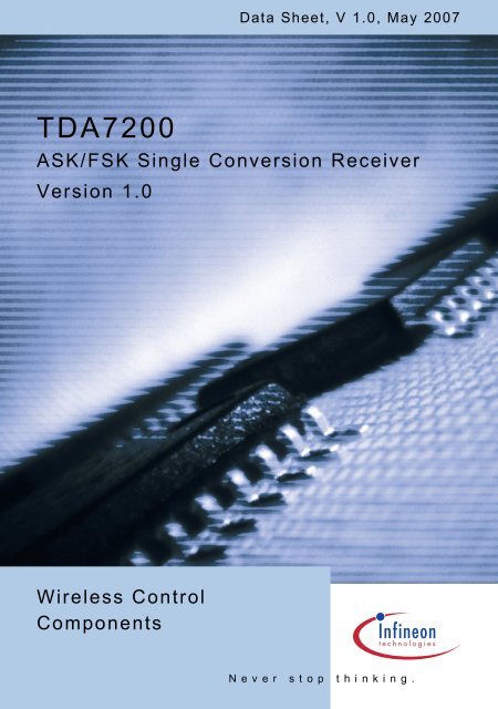
Data Sheet, V 1.0, May 2007<br />
<strong>TDA7200</strong><br />
ASK/FSK Single Conversion Receiver<br />
Version 1.0<br />
Wireless Control<br />
Components<br />
Never stop thinking.
Edition 2007-05-02<br />
Published by <strong>Infineon</strong> Technologies AG,<br />
Am Campeon 1-12,<br />
85579 Neubiberg, Germany<br />
© <strong>Infineon</strong> Technologies AG 2007-05-02.<br />
All Rights Reserved.<br />
Attention please!<br />
The information herein is given to describe certain components and shall not be considered as a guarantee of<br />
characteristics.<br />
Terms of delivery and rights to technical change reserved.<br />
We hereby disclaim any and all warranties, including but not limited to warranties of non-infringement, regarding<br />
circuits, descriptions and charts stated herein.<br />
Information<br />
For further information on technology, delivery terms and conditions and prices please contact your nearest<br />
<strong>Infineon</strong> Technologies Office in Germany or the <strong>Infineon</strong> Technologies Companies and our <strong>Infineon</strong> Technologies<br />
Representatives worldwide (www.infineon.com).<br />
Warnings<br />
Due to technical requirements components may contain dangerous substances. For information on the types in<br />
question please contact your nearest <strong>Infineon</strong> Technologies Office.<br />
<strong>Infineon</strong> Technologies Components may only be used in life-support devices or systems with the express written<br />
approval of <strong>Infineon</strong> Technologies, if a failure of such components can reasonably be expected to cause the failure<br />
of that life-support device or system, or to affect the safety or effectiveness of that device or system. Life support<br />
devices or systems are intended to be implanted in the human body, or to support and/or maintain and sustain<br />
and/or protect human life. If they fail, it is reasonable to assume that the health of the user or other persons may<br />
be endangered.
Data Sheet, V 1.0, May 2007<br />
<strong>TDA7200</strong><br />
ASK/FSK Single Conversion Receiver<br />
Version 1.0<br />
Wireless Control<br />
Components<br />
Never stop thinking.
<strong>TDA7200</strong><br />
Revision History: 2007-05-02 V 1.0<br />
Previous Version: none<br />
Page Subjects (major changes since last revision)<br />
We Listen to Your Comments<br />
Any information within this document that you feel is wrong, unclear or missing at all?<br />
Your feedback will help us to continuously improve the quality of this document.<br />
Please send your proposal (including a reference to this document) to:<br />
sensors@infineon.com
<strong>TDA7200</strong><br />
Table of Contents<br />
Page<br />
1 Product Description . . . . . . . . . . . . . . . . . . . . . . . . . . . . . . . . . . . . . . . . . 6<br />
1.1 Overview . . . . . . . . . . . . . . . . . . . . . . . . . . . . . . . . . . . . . . . . . . . . . . . . . . . 6<br />
1.2 Features . . . . . . . . . . . . . . . . . . . . . . . . . . . . . . . . . . . . . . . . . . . . . . . . . . . . 6<br />
1.3 Application . . . . . . . . . . . . . . . . . . . . . . . . . . . . . . . . . . . . . . . . . . . . . . . . . . 6<br />
2 Functional Description . . . . . . . . . . . . . . . . . . . . . . . . . . . . . . . . . . . . . . . 7<br />
2.1 Pin Configuration . . . . . . . . . . . . . . . . . . . . . . . . . . . . . . . . . . . . . . . . . . . . . 7<br />
2.2 Pin Definition and Functions . . . . . . . . . . . . . . . . . . . . . . . . . . . . . . . . . . . . 8<br />
2.3 Functional Block Diagram . . . . . . . . . . . . . . . . . . . . . . . . . . . . . . . . . . . . . 15<br />
2.4 Functional Block Description . . . . . . . . . . . . . . . . . . . . . . . . . . . . . . . . . . . 15<br />
2.4.1 Low Noise Amplifier (LNA) . . . . . . . . . . . . . . . . . . . . . . . . . . . . . . . . . . . 15<br />
2.4.2 Mixer . . . . . . . . . . . . . . . . . . . . . . . . . . . . . . . . . . . . . . . . . . . . . . . . . . . 16<br />
2.4.3 PLL Synthesizer . . . . . . . . . . . . . . . . . . . . . . . . . . . . . . . . . . . . . . . . . . . 16<br />
2.4.4 Crystal Oscillator . . . . . . . . . . . . . . . . . . . . . . . . . . . . . . . . . . . . . . . . . . 16<br />
2.4.5 Limiter . . . . . . . . . . . . . . . . . . . . . . . . . . . . . . . . . . . . . . . . . . . . . . . . . . 16<br />
2.4.6 FSK Demodulator . . . . . . . . . . . . . . . . . . . . . . . . . . . . . . . . . . . . . . . . . 17<br />
2.4.7 Data Filter . . . . . . . . . . . . . . . . . . . . . . . . . . . . . . . . . . . . . . . . . . . . . . . 17<br />
2.4.8 Data Slicer . . . . . . . . . . . . . . . . . . . . . . . . . . . . . . . . . . . . . . . . . . . . . . . 18<br />
2.4.9 Peak Detector . . . . . . . . . . . . . . . . . . . . . . . . . . . . . . . . . . . . . . . . . . . . 18<br />
2.4.10 Bandgap Reference Circuitry . . . . . . . . . . . . . . . . . . . . . . . . . . . . . . . . . 18<br />
3 Applications . . . . . . . . . . . . . . . . . . . . . . . . . . . . . . . . . . . . . . . . . . . . . . . 19<br />
3.1 Application Circuit . . . . . . . . . . . . . . . . . . . . . . . . . . . . . . . . . . . . . . . . . . . 19<br />
3.2 Data Filter Design . . . . . . . . . . . . . . . . . . . . . . . . . . . . . . . . . . . . . . . . . . . 21<br />
3.3 Crystal Load Capacitance Calculation . . . . . . . . . . . . . . . . . . . . . . . . . . . . 22<br />
3.4 Crystal Frequency Calculation . . . . . . . . . . . . . . . . . . . . . . . . . . . . . . . . . . 22<br />
3.5 Data Slicer Threshold Generation . . . . . . . . . . . . . . . . . . . . . . . . . . . . . . . 23<br />
3.6 ASK/FSK-Data Path Functional Description . . . . . . . . . . . . . . . . . . . . . . . 25<br />
3.7 FSK Mode . . . . . . . . . . . . . . . . . . . . . . . . . . . . . . . . . . . . . . . . . . . . . . . . . 26<br />
3.8 ASK Mode . . . . . . . . . . . . . . . . . . . . . . . . . . . . . . . . . . . . . . . . . . . . . . . . . 28<br />
3.9 Principle of the Precharge Circuit . . . . . . . . . . . . . . . . . . . . . . . . . . . . . . . 28<br />
4 Reference . . . . . . . . . . . . . . . . . . . . . . . . . . . . . . . . . . . . . . . . . . . . . . . . . 32<br />
4.1 Electrical Data . . . . . . . . . . . . . . . . . . . . . . . . . . . . . . . . . . . . . . . . . . . . . . 32<br />
4.1.1 Absolute Maximum Ratings . . . . . . . . . . . . . . . . . . . . . . . . . . . . . . . . . . 32<br />
4.1.2 Operating Range . . . . . . . . . . . . . . . . . . . . . . . . . . . . . . . . . . . . . . . . . . 32<br />
4.1.3 AC/DC Characteristics at T AMB = 25°C . . . . . . . . . . . . . . . . . . . . . . . . . 33<br />
4.1.4 AC/DC Characteristics at T AMB = -20°C ... +70°C . . . . . . . . . . . . . . . . . . 38<br />
4.2 Test Circuit . . . . . . . . . . . . . . . . . . . . . . . . . . . . . . . . . . . . . . . . . . . . . . . . . 42<br />
4.3 Test Board Layouts . . . . . . . . . . . . . . . . . . . . . . . . . . . . . . . . . . . . . . . . . . 43<br />
4.4 Bill of Materials . . . . . . . . . . . . . . . . . . . . . . . . . . . . . . . . . . . . . . . . . . . . . 44<br />
5 Package Outlines . . . . . . . . . . . . . . . . . . . . . . . . . . . . . . . . . . . . . . . . . . . 46<br />
Data Sheet 5 V 1.0, 2007-05-02
<strong>TDA7200</strong><br />
Product Description<br />
1 Product Description<br />
1.1 Overview<br />
The IC is a very low power consumption single chip FSK/ASK Superheterodyne<br />
Receiver (SHR) for the frequency band 400 to 440 MHz. The IC offers a high level of<br />
integration and needs only a few external components. The device contains a low noise<br />
amplifier (LNA), a double balanced mixer, a fully integrated VCO, a PLL synthesiser, a<br />
crystal oscillator, a limiter with RSSI generator, a PLL FSK demodulator, a data filter, an<br />
advanced data comparator (slicer) with selection between two threshold modes and a<br />
peak detector. Additionally there is a power down feature to save current and extend<br />
battery life, and two selectable alternatives of generating the data slicer threshold.<br />
1.2 Features<br />
• Low supply current (Is = 5.7 mA typ. in FSK mode, Is = 5.0 mA typ. in ASK mode)<br />
• Supply voltage range 5V ±10%<br />
• Power down mode with very low supply current (50nA typ.)<br />
• FSK and ASK demodulation capability<br />
• Fully integrated VCO and PLL Synthesiser<br />
• ASK sensitivity better than -106 dBm over specified temperature range (-20 to<br />
+70°C)<br />
• FSK sensitivity better than -100 dBm over specified temperature range (-20 to +70°C)<br />
• Limiter with RSSI generation, operating at 10.7MHz<br />
• 2nd order low pass data filter with external capacitors<br />
• Data slicer with selection between two threshold modes (see Section 2.4.8)<br />
1.3 Application<br />
• Remote Control Systems<br />
• Alarm Systems<br />
• Low Bitrate Communication Systems<br />
Table 1<br />
Order Information<br />
Type Ordering Code Package<br />
<strong>TDA7200</strong> SP000296473 PG-TSSOP-28<br />
Data Sheet 6 V 1.0, 2007-05-02
<strong>TDA7200</strong><br />
Functional Description<br />
2 Functional Description<br />
2.1 Pin Configuration<br />
CRST1<br />
1<br />
28<br />
CRST2<br />
VCC<br />
2<br />
27<br />
PDWN<br />
LNI<br />
3<br />
26<br />
PDO<br />
TAGC<br />
4<br />
25<br />
DATA<br />
AGND<br />
5<br />
24<br />
3VOUT<br />
LNO<br />
6<br />
23<br />
THRES<br />
VCC<br />
MI<br />
7<br />
8<br />
TDA 7200<br />
22<br />
21<br />
FFB<br />
OPP<br />
MIX<br />
9<br />
20<br />
SLN<br />
AGND<br />
10<br />
19<br />
SLP<br />
PTST<br />
11<br />
18<br />
LIMX<br />
IFO<br />
12<br />
17<br />
LIM<br />
DGND<br />
13<br />
16<br />
SSEL<br />
VDD<br />
14<br />
15<br />
MSEL<br />
Figure 1<br />
Pin Configuration<br />
Data Sheet 7 V 1.0, 2007-05-02
<strong>TDA7200</strong><br />
Functional Description<br />
2.2 Pin Definition and Functions<br />
Table 2<br />
Pin Defintion and Function<br />
Pin Symbol Equivalent I/O Schematic Function<br />
No.<br />
1 CRST1 External Crystal<br />
Connector 1<br />
4.15V<br />
1<br />
50uA<br />
2 VCC 5V Supply<br />
3 LNI LNA Input<br />
57uA<br />
3<br />
4k<br />
500uA<br />
1k<br />
Data Sheet 8 V 1.0, 2007-05-02
<strong>TDA7200</strong><br />
Pin<br />
No.<br />
Functional Description<br />
Symbol Equivalent I/O Schematic Function<br />
4 TAGC AGC Time<br />
Constant Control<br />
4.3V<br />
4.2uA<br />
4<br />
1k<br />
1.5uA<br />
5 AGND Analogue<br />
Ground Return<br />
6 LNO LNA Output<br />
1.7V<br />
5V<br />
1k<br />
6<br />
7 VCC 5V Supply<br />
Data Sheet 9 V 1.0, 2007-05-02
<strong>TDA7200</strong><br />
Pin<br />
No.<br />
Functional Description<br />
Symbol Equivalent I/O Schematic Function<br />
8 MI Mixer Input<br />
9 MIX<br />
1.7V<br />
Complementary<br />
Mixer Input<br />
2k<br />
2k<br />
8<br />
9<br />
400uA<br />
10 AGND Analogue<br />
Ground Return<br />
11 PTST has to be left<br />
open<br />
12 IFO 10.7 MHz IF<br />
Mixer Output<br />
300uA<br />
2.2V<br />
12<br />
60<br />
4.5k<br />
13 DGND Digital Ground<br />
Return<br />
14 VDD 5V Supply (PLL<br />
Counter Circuity)<br />
Data Sheet 10 V 1.0, 2007-05-02
<strong>TDA7200</strong><br />
Pin<br />
No.<br />
Functional Description<br />
Symbol Equivalent I/O Schematic Function<br />
15 MSEL ASK/FSK<br />
Modulation<br />
Format Sector<br />
1.2V<br />
15<br />
40k<br />
16 SSEL Data Slicer<br />
Reference Level<br />
Sector<br />
1.2V<br />
16<br />
40k<br />
17 LIM Limiter Input<br />
18 LIMX<br />
2.4V<br />
Complementary<br />
Limiter Input<br />
15k<br />
17<br />
330<br />
75uA<br />
18<br />
15k<br />
Data Sheet 11 V 1.0, 2007-05-02
<strong>TDA7200</strong><br />
Pin<br />
No.<br />
Functional Description<br />
Symbol Equivalent I/O Schematic Function<br />
19 SLP Data Slicer<br />
Positive Input<br />
15uA<br />
19<br />
100<br />
3k<br />
80µA<br />
20 SLN Data Slicer<br />
Negative Input<br />
5uA<br />
20<br />
10k<br />
21 OPP OpAmp<br />
Noninverting<br />
Input<br />
5uA<br />
21<br />
200<br />
22 FFB Data Filter<br />
Feedback Pin<br />
5uA<br />
22<br />
100k<br />
Data Sheet 12 V 1.0, 2007-05-02
<strong>TDA7200</strong><br />
Pin<br />
No.<br />
Functional Description<br />
Symbol Equivalent I/O Schematic Function<br />
23 THRES AGC Threshold<br />
Input<br />
5uA<br />
23<br />
10k<br />
24 3VOUT 3V Reference<br />
Output<br />
24<br />
20kΩ<br />
3.1V<br />
25 DATA Data Output<br />
25<br />
500<br />
40k<br />
26 PDO Peak Detector<br />
Output<br />
26<br />
446k<br />
Data Sheet 13 V 1.0, 2007-05-02
<strong>TDA7200</strong><br />
Pin<br />
No.<br />
Functional Description<br />
Symbol Equivalent I/O Schematic Function<br />
27 PDWN Power Down<br />
Input<br />
27<br />
220k<br />
220k<br />
28 CRST2 External Crystal<br />
Connector 2<br />
4.15V<br />
28<br />
50uA<br />
Data Sheet 14 V 1.0, 2007-05-02
<strong>TDA7200</strong><br />
Functional Description<br />
2.3 Functional Block Diagram<br />
VCC<br />
IF<br />
Filter<br />
MSEL<br />
H=ASK<br />
L=FSK<br />
RF<br />
TAGC<br />
VCC<br />
LNI<br />
3<br />
4<br />
14<br />
LNA<br />
MI<br />
LIM<br />
LNO MI IFO LIM<br />
FFB OPP<br />
X<br />
X<br />
6 8 9 12 17 18 15<br />
22 21 19 20<br />
TDA 7200<br />
OTA<br />
: 2 VCO : 64<br />
LIMITER<br />
Φ<br />
DET<br />
FSK<br />
PLL Demod<br />
-<br />
+ FSK<br />
-ASK<br />
+<br />
CRYSTAL<br />
OSC<br />
+<br />
-<br />
OP<br />
SLP<br />
SLN<br />
-<br />
+ CM<br />
AGC<br />
Reference<br />
Logic<br />
+ CP<br />
-<br />
DATA-<br />
SLICER<br />
PEAK<br />
DETECTOR<br />
U REF<br />
16<br />
25<br />
26<br />
23<br />
24<br />
SSEL<br />
DATA<br />
PDO<br />
THRES<br />
3VOUT<br />
DGND<br />
13<br />
Loop<br />
Filter<br />
Bandgap<br />
Reference<br />
2,7 5,10<br />
1 28 11<br />
27<br />
VCC<br />
AGND<br />
PTST<br />
PDWN<br />
Crystal<br />
Figure 2<br />
Block Diagram<br />
2.4 Functional Block Description<br />
2.4.1 Low Noise Amplifier (LNA)<br />
The LNA is an on-chip cascode amplifier with a voltage gain of 15 to 20dB. The gain<br />
figure is determined by the external matching networks situated ahead of LNA and<br />
between the LNA output LNO (Pin 6) and the Mixer Inputs MI and MIX (Pins 8 and 9).<br />
The noise figure of the LNA is approximately 3dB, the current consumption is 500µA.<br />
The gain can be reduced by approximately 18dB. The switching point of this AGC action<br />
can be determined externally by applying a threshold voltage at the THRES pin (Pin 23).<br />
This voltage is compared internally with the received signal (RSSI) level generated by<br />
the limiter circuitry. In case that the RSSI level is higher than the threshold voltage the<br />
LNA gain is reduced and vice versa. The threshold voltage can be generated by<br />
attaching a voltage divider between the 3VOUT pin (Pin 24) which provides a<br />
temperature stable 3V output generated from the internal bandgap voltage and the<br />
THRES pin as described in Section 3.1. The time constant of the AGC action can be<br />
determined by connecting a capacitor to the TAGC pin (Pin 4) and should be chosen<br />
along with the appropriate threshold voltage according to the intended operating case<br />
and interference scenario to be expected during operation. The optimum choice of AGC<br />
time constant and the threshold voltage is described in Section 3.1.<br />
Data Sheet 15 V 1.0, 2007-05-02
<strong>TDA7200</strong><br />
2.4.2 Mixer<br />
Functional Description<br />
The Double Balanced Mixer downconverts the input frequency (RF) in the range of 400-<br />
440MHz to the intermediate frequency (IF) at 10.7MHz with a voltage gain of<br />
approximately 21dB by utilising either high- or low-side injection of the local oscillator<br />
signal. In case the mixer is interfaced only single-ended, the unused mixer input has to<br />
be tied to ground via a capacitor. The mixer is followed by a low pass filter with a corner<br />
frequency of 20MHz in order to suppress RF signals to appear at the IF output (IFO pin).<br />
The IF output is internally consisting of an emitter follower that has a source impedance<br />
of approximately 330Ω to facilitate interfacing the pin directly to a standard 10.7MHz<br />
ceramic filter without additional matching circuitry.<br />
2.4.3 PLL Synthesizer<br />
The Phase Locked Loop synthesizer consists of a VCO, an asynchronous divider chain,<br />
a phase detector with charge pump and a loop filter and is fully implemented on-chip.<br />
The VCO is including spiral inductors and varactor diodes. The frequency range of the<br />
VCO guaranteed over production spread and the specified temperature range is 820 to<br />
860MHz. The oscillator signal is fed both to the synthesiser divider chain and to the<br />
downconverting mixer. The VCO signal is divided by two before it is fed to the Mixer.<br />
Depending on whether high- or low-side injection of the local oscillator is used, the<br />
receiving frequency range is 400 to 420MHz and 420 to 440MHz - see also Section 3.4.<br />
2.4.4 Crystal Oscillator<br />
The calculation of the value of the necessary crystal load capacitance is shown in<br />
Section 3.3, the crystal frequency calculation is explained in Section 3.4.<br />
2.4.5 Limiter<br />
The Limiter is an AC coupled multistage amplifier with a cumulative gain of<br />
approximately 80 dB that has a bandpass-characteristic centred around 10.7 MHz. It<br />
has a typical input impedance of 330 Ω to allow for easy interfacing to a 10.7 MHz<br />
ceramic IF filter. The limiter circuit also acts as a Receive Signal Strength Indicator<br />
(RSSI) generator which produces a DC voltage that is directly proportional to the input<br />
signal level as can be seen in Figure 4. This signal is used to demodulate ASKmodulated<br />
receive signals in the subsequent baseband circuitry. The RSSI output is<br />
applied to the modulation format switch, to the Peak Detector input and to the AGC<br />
circuitry.<br />
In order to demodulate ASK signals the MSEL pin has to be in its ‘High‘-state as<br />
described in the next chapter.<br />
Data Sheet 16 V 1.0, 2007-05-02
<strong>TDA7200</strong><br />
2.4.6 FSK Demodulator<br />
Functional Description<br />
To demodulate frequency shift keyed (FSK) signals a PLL circuit is used that is<br />
contained fully on chip. The Limiter output differential signal is fed to the linear phase<br />
detector as is the output of the 10.7 MHz center frequency VCO. The demodulator gain<br />
is typically 200µV/kHz. The passive loop filter output that is comprised fully on chip is fed<br />
to both the VCO and the modulation format switch described in more detail below. This<br />
signal is representing the demodulated signal with low frequencies applied to the<br />
demodulator demodulated to logic zero and high frequencies demodulated to logic ones.<br />
However this is only valid in case the local oscillator is low-side injected to the mixer<br />
which is applicable to receive frequencies above 420MHz. In case of receive frequencies<br />
below 420MHz high frequencies are demodulated as logical zeroes due to a sign<br />
inversion in the downconversion mixing process as the L0 is high-side injected to the<br />
mixer. See also Section 3.4.<br />
The modulation format switch is actually a switchable amplifier with an AC gain of 11 that<br />
is controlled by the MSEL pin (Pin 15) as shown in the following table. This gain was<br />
chosen to facilitate detection in the subsequent circuits. The DC gain is 1 in order not to<br />
saturate the subsequent Data Filter wih the DC offset produced by the demodulator in<br />
case of large frequency offsets of the IF signal. The resulting frequency characteristic<br />
and details on the principle of operation of the switch are described in Section 3.6.<br />
Table 3<br />
MSEL Pin Operating States<br />
MSEL<br />
Open<br />
Shorted to ground<br />
Modulation Format<br />
ASK<br />
FSK<br />
The demodulator circuit is switched off in case of reception of ASK signals.<br />
2.4.7 Data Filter<br />
The data filter comprises an OP-Amp with a bandwidth of 100kHz used as a voltage<br />
follower and two 100kΩ on-chip resistors. Along with two external capacitors a 2nd order<br />
Sallen-Key low pass filter is formed. The selection of the capacitor values is described<br />
in Section 3.2.<br />
Data Sheet 17 V 1.0, 2007-05-02
<strong>TDA7200</strong><br />
2.4.8 Data Slicer<br />
Functional Description<br />
The data slicer is a fast comparator with a bandwidth of 100 kHz. This allows for a<br />
maximum receive data rate of up to 100kBaud. The maximum achievable data rate also<br />
depends on the IF Filter bandwidth and the local oscillator tolerance values. Both inputs<br />
are accessible. The output delivers a digital data signal (CMOS-like levels) for<br />
subsequent circuits. A self-adjusting slicer-threshold on pin 20 its generated by a RCterm.<br />
In ASK-mode alternatively a scaled value of the voltage at the PDO-output (approx.<br />
87%) can be used as the slicer-threshold as shown in Table 4. The data slicer threshold<br />
generation alternatives are described in more detail in Section 3.5.<br />
Table 4<br />
SSEL Pin Operating States<br />
SSEL MSEL Selected Slicing Level (SL)<br />
X Low external SL on Pin 20 (RC-term, e.g.)<br />
High High external SL on Pin 20 (RC-term, e.g.)<br />
Low High 87% of PDO-output (approx.)<br />
2.4.9 Peak Detector<br />
The peak detector generates a DC voltage which is proportional to the peak value of the<br />
receive data signal. A capacitor is necessary. The input is connected to the output of the<br />
RSSI-output of the Limiter, the output is connected to the PDO pin (Pin 26). This output<br />
can be used as an indicator for the received signal strength to use in wake-up circuits<br />
and as a reference for the data slicer in ASK mode. Note that the RSSI level is also<br />
output in case of FSK mode.<br />
2.4.10 Bandgap Reference Circuitry<br />
A Bandgap Reference Circuit provides a temperature stable reference voltage for the<br />
device. A power down mode is available to switch off all subcircuits which is controlled<br />
by the PWDN pin (Pin 27) as shown in the following table. The supply current drawn in<br />
this case is typically 50nA.<br />
Table 5<br />
PDWN Pin Operating States<br />
PDWN<br />
Open or tied to ground<br />
Tied to Vs<br />
Operating State<br />
Powerdown Mode<br />
Receiver On<br />
Data Sheet 18 V 1.0, 2007-05-02
<strong>TDA7200</strong><br />
Applications<br />
3 Applications<br />
3.1 Application Circuit<br />
C18<br />
R4<br />
R5<br />
U threshold<br />
3VOUT<br />
THRES<br />
24 23<br />
20kΩ<br />
RSSI (0.8 - 2.8V)<br />
+3.1 V<br />
OTA<br />
VCC<br />
RSSI > U threshold<br />
: I load<br />
=4.2µA<br />
RSSI < U threshold<br />
: I load<br />
= -1.5µA<br />
4<br />
I load<br />
Gain control<br />
voltage<br />
LNA<br />
TAGC<br />
U C<br />
U c<br />
:< 2.6V : Gain high<br />
U c<br />
:> 2.6V : Gain low<br />
C5<br />
U cmax<br />
= V CC<br />
- 0.7V<br />
U cmin<br />
= 1.67V<br />
Figure 3<br />
LNA Automatic Gain Control Circuity<br />
The LNA automatic gain control circuitry consists of an operational transimpedance<br />
amplifier that is used to compare the received signal strength signal (RSSI) generated<br />
by the Limiter with an externally provided threshold voltage U thres . As shown in the<br />
following figure the threshold voltage can have any value between approximately 0.8 and<br />
2.8V to provide a switching point within the receive signal dynamic range.<br />
This voltage U thres is applied to the THRES pin (Pin 23) The threshold voltage can be<br />
generated by attaching a voltage divider between the 3VOUT pin<br />
(Pin 24) which provides a temperature stable 3V output generated from the internal<br />
bandgap voltage and the THRES pin. If the RSSI level generated by the Limiter is higher<br />
than U thres , the OTA generates a positive current I load . This yields a voltage rise on the<br />
TAGC pin (Pin 4). Otherwise, the OTA generates a negative current. These currents do<br />
not have the same values in order to achieve a fast-attack and slow-release action of the<br />
Data Sheet 19 V 1.0, 2007-05-02
<strong>TDA7200</strong><br />
Applications<br />
AGC and are used to charge an external capacitor which finally generates the LNA gain<br />
control voltage.<br />
3<br />
2.5<br />
LNA always<br />
in high gain mode<br />
U THRES Voltage Range<br />
2<br />
RSSI Level<br />
1.5<br />
1<br />
0.5<br />
0<br />
-120 -110 -100 -90 -80 -70 -60 -50 -40 -30<br />
Input Level at LNA Input [dBm]<br />
RSSI Level Range LNA always<br />
in low gain mode<br />
Figure 4<br />
RSSI Level and Permissive AGC Threshold Levels<br />
The switching point should be chosen according to the intended operating scenario. The<br />
determination of the optimum point is described in the accompanying Application Note,<br />
a threshold voltage level of 1.8V is apparently a viable choice. It should be noted that the<br />
output of the 3VOUT pin is capable of driving up to 50µA, but that the THRES pin input<br />
current is only in the region of 40nA. As the current drawn out of the 3VOUT pin is directly<br />
related to the receiver power consumption, the power divider resistors should have high<br />
impedance values. The sum of R1 and R2 has to be 600kΩ in order to yield 3V at the<br />
3VOUT pin. R1 can thus be chosen as 240kΩ, R2 as 360kΩ to yield an overall 3VOUT<br />
output current of 5µA 1) and a threshold voltage of 1.8V<br />
Note: If the LNA gain shall be kept in either high or low gain mode this has to be<br />
accomplished by tying the THRES pin to a fixed voltage. In order to achieve high gain<br />
mode operation, a voltage higher than 2.8V shall be applied to the THRES pin, such as<br />
a short to the 3VOLT pin. In order to achieve low gain mode operation THRES has to be<br />
connected to GND.<br />
As stated above the capacitor connected to the TAGC pin is generating the gain control<br />
voltage of the LNA due to the charging and discharging currents of the OTA and thus is<br />
also responsible for the AGC time constant. As the charging and discharging currents<br />
are not equal two different time constants will result. The time constant corresponding to<br />
the charging process of the capacitor shall be chosen according to the data rate.<br />
According to measurements performed at <strong>Infineon</strong> the capacitor value should be greater<br />
than 47nF.<br />
1) note the 20kΩ resistor in series with the 3.1V internal voltage source<br />
Data Sheet 20 V 1.0, 2007-05-02
<strong>TDA7200</strong><br />
Applications<br />
3.2 Data Filter Design<br />
Utilising the on-board voltage follower and the two 100kΩ on-chip resistors a 2nd order<br />
Sallen-Key low pass data filter can be constructed by adding 2 external capacitors<br />
between pins 19 (SLP) and 22 (FFB) and to pin 21 (OPP) as depicted in the following<br />
figure and described in the following formulas 1) .<br />
C14<br />
C12<br />
R F1 int<br />
FFB<br />
22 21 19<br />
R F2 int<br />
OPP<br />
SLP<br />
100k<br />
100k<br />
Figure 5<br />
Data Filter Design<br />
with R F1int =R F2int =R<br />
2Q<br />
b<br />
C14<br />
=<br />
R2πf<br />
3dB<br />
b<br />
C12<br />
=<br />
4QRπf<br />
3dB<br />
with<br />
Q =<br />
b<br />
a<br />
Q is the qualify factor of the poles where, in case of a Bessel filter a=1.3617, b=0.618<br />
and thus Q=0.577<br />
and in case of a Butter worth filter a=1.414, b=1<br />
and thus Q=0.71<br />
Example: Butter worth filter with f 3dB =5kHz and R=100kΩ:<br />
C14=450pF, C12=225pF<br />
1) taken from Tietze/Schenk: Halbleiterschaltungstechnik, Springer Berlin, 1999<br />
Data Sheet 21 V 1.0, 2007-05-02
<strong>TDA7200</strong><br />
Applications<br />
3.3 Crystal Load Capacitance Calculation<br />
The value of the capacitor necessary to achieve that the crystal oscillator is operating at<br />
the intended frequency is determined by the reactive part of the negative resistance of<br />
the oscillator circuit as shown in Section 4.1.3 and by the crystal specifications given by<br />
the crystal manufacturer.<br />
C S<br />
CRST2<br />
Crystal<br />
Input<br />
impedance<br />
Z 1-28<br />
28<br />
<strong>TDA7200</strong><br />
1<br />
CRST1<br />
Figure 6<br />
Determination of Series Capacitance Vale for the Quartz Oscillator<br />
The required series capacitor for a crystal with specified load capacitance C L can be<br />
calculated as<br />
CS<br />
=<br />
1<br />
C<br />
L<br />
1<br />
+ 2π f X<br />
L<br />
C L is the nominal load capacitance specified by the crystal manufacturer.<br />
Example:<br />
13.4 MHz: C L = 12 pF X L =1010 Ω C S = 5.9 pF<br />
This value may be obtained by putting two capacitors in series to the crystal, such as<br />
22pF and 8.2pF for 13.4MHz.<br />
But please note that the calculated C S -value includes all parasitic.<br />
3.4 Crystal Frequency Calculation<br />
As described in Section 2.4.3 the operating range of the on-chip VCO is wide enough to<br />
guarantee a receive frequency range between 400 and 440MHz. The VCO signal is<br />
divided by 2 before applied to the mixer. This local oscillator signal can be used to<br />
downconvert the RF signals both with high- or low-side injection at the mixer. High-side<br />
Data Sheet 22 V 1.0, 2007-05-02
<strong>TDA7200</strong><br />
Applications<br />
injection of the local oscillator has to be used for receive frequencies between 400 and<br />
420MHz. In this case the local oscillator frequency is calculated by adding the IF<br />
frequency (10.7 MHz) to the RF frequency. Thus the higher frequency of a FSKmodulated<br />
signal is demodulated as a logical zero (low).<br />
Low-side injection has to be used for receive frequencies above 420 MHz. The local<br />
oscillator frequency is calculated by subtracting the IF frequency (10.7 MHz) from the RF<br />
frequency then. In this case no sign-inversion occurs and the higher frequency of a FSKmodulated<br />
signal is demodulated as a logical one (high). The overall division ratio in the<br />
PLL is 32.<br />
Therefore the crystal frequency may be calculated by using the following formula:<br />
f<br />
QU<br />
f<br />
= RF<br />
±10.7<br />
32<br />
with<br />
ƒ RF receive frequency<br />
ƒ LO local oscillator (PLL) frequency (ƒ RF ± 10.7)<br />
ƒ QU quartz crystal oscillator frequency<br />
32 ratio of local oscillator (PLL) frequency and crystal frequency.<br />
This yields the following example:<br />
434 .2MHz<br />
− 10.7MHz<br />
f QU =<br />
= 13. 234375 MHz<br />
32<br />
3.5 Data Slicer Threshold Generation<br />
The threshold of the data slicer can be generated using an external R-C integrator as<br />
shown in Figure 7.<br />
The time constant T A of this circuit including also the internal resistors R F3int and R F4int<br />
(see Figure 9) has to be significantly larger than the longest period of no signal change<br />
T L within the data sequence.<br />
In order to keep distortion low, the minimum value for R is 20kΩ.<br />
Data Sheet 23 V 1.0, 2007-05-02
<strong>TDA7200</strong><br />
Applications<br />
T A has to be calculated as<br />
T<br />
A<br />
=<br />
R1⋅<br />
( R<br />
R1<br />
+ R<br />
F 3int<br />
F 3int<br />
+ R<br />
+ R<br />
F 4int<br />
F 4int<br />
)<br />
⋅C13<br />
= R1II(<br />
R<br />
F 3int<br />
+ R<br />
F 4int<br />
) ⋅C13<br />
... for<br />
ASK<br />
and<br />
T<br />
A<br />
=<br />
R1<br />
+ R<br />
R1⋅<br />
R<br />
F 3int<br />
F 4int<br />
+ R<br />
F 4int<br />
⋅C13<br />
=<br />
R1II<br />
( R<br />
F 3int<br />
v<br />
+ R<br />
F 4int<br />
)<br />
⋅C13<br />
... for<br />
FSK<br />
R1, R F3 int , R F4 int and C13 see also Figure 7 and Figure 9<br />
19 20 U threshold 25<br />
data<br />
filter<br />
CM<br />
data slicer<br />
Figure 7<br />
Data Slicer Threshold Generation with External R-C Integrator<br />
In case of ASK operation another possibility for threshold generation is to use the peak<br />
detector in connection with an internal resistive divider and one capacitor as shown in<br />
Figure 8. For selecting the peak detector as reference for the slicing level a logic low as<br />
to be applied on the SSEL pin.<br />
In case of MSEL is high (or open), which means that ASK-Mode is selected, a logic low<br />
on the SSEL pin yields a logic high on the AND-output and thus the peak-detector is<br />
selected (see Figure 9).<br />
In case of FSK the MSEL-pin and furthermore the one input of the AND-gate is low, so<br />
the peak detector can not be selected.<br />
The capacitor value is depending on the coding scheme and the protocol used.<br />
Data Sheet 24 V 1.0, 2007-05-02
<strong>TDA7200</strong><br />
Applications<br />
C<br />
Pins: 26<br />
25<br />
peak detector<br />
56k<br />
390k<br />
U threshold<br />
data slicer<br />
CP<br />
Figure 8<br />
Data Slicer Threshold Generation Utilising the Peak Detector<br />
3.6 ASK/FSK-Data Path Functional Description<br />
The <strong>TDA7200</strong> is containing an ASK/FSK switch which can be controlled via Pin 15<br />
(MSEL). This switch is actually consisting of 2 operational amplifiers that are having a<br />
gain of 1 in case of the ASK amplifier and a gain of 11 in case of the FSK amplifier in<br />
order to achieve an appropriate demodulation gain characteristic. In order to<br />
compensate for the DC-offset generated especially in case of the FSK PLL demodulator<br />
there is a feedback connection between the threshold voltage of the bit slicer comparator<br />
(Pin 20) to the negative input of the FSK switch amplifier.<br />
In ASK-mode alternatively to the voltage at Pin 20 (SLN) a value of approx. 87% of the<br />
peak-detector output-voltage at Pin 26 (PDO) can be used as the slicer-reference level.<br />
The slicing reference level is generated by an internal voltage divider (R T1int , R T2int ),<br />
which is applied on the peak detector output.<br />
The selection between these modes is controlled by Pin 16 (SSEL), as described in<br />
Section 3.5.<br />
This is shown in Figure 9.<br />
Data Sheet 25 V 1.0, 2007-05-02
1<br />
<strong>TDA7200</strong><br />
Applications<br />
MSEL<br />
15<br />
from RSSI Gen<br />
(ASK signal)<br />
ASK/FSK Switch<br />
H=ASK<br />
L=FSK<br />
PEAK<br />
DETECTOR<br />
R T1 int<br />
26<br />
56k<br />
PDO<br />
C15<br />
100nF<br />
FSK PLL Demodulator<br />
0.18 mV/kHz<br />
typ. 2 V<br />
1.5 V......2.5 V<br />
AC DC<br />
+ - ASK<br />
+ FSK<br />
- R F3 int<br />
R F4 int<br />
30k<br />
300k<br />
R F1 int R F2 int<br />
v = 1<br />
100k<br />
100k<br />
Data Filter<br />
R T2<br />
390k<br />
Comp<br />
-<br />
+ CP<br />
25<br />
+ CM<br />
- H=CP<br />
L=CM<br />
DATA Out<br />
ASK mode: v=1<br />
FSK mode: v=11<br />
22 21<br />
19<br />
20<br />
FFB OOP<br />
SLP<br />
16<br />
SLN<br />
SSEL<br />
C12<br />
C14<br />
R1<br />
C13<br />
Figure 9<br />
ASK/FSK mode datapath<br />
3.7 FSK Mode<br />
The FSK datapath has a bandpass characterisitc due to the feedback shown above<br />
(highpass) and the data filter (lowpass). The lower cutoff frequency f2 is determined by<br />
the external RC-combination. The upper cutoff frequency f3 is determined by the data<br />
filter bandwidth.<br />
The demodulation gain of the FSK PLL demodulator is 200µV/kHz. This gain is<br />
increased by the gain v of the FSK switch, which is 11. Therefore the resulting dynamic<br />
gain of this circuit is 2.2mV/kHz within the bandpass. The gain for the DC content of FSK<br />
signal remains at 200µV/kHz. The cut-off frequencies of the bandpass have to be chosen<br />
such that the spectrum of the data signal is influenced in an acceptable amount.<br />
In case that the user data is containing long sequences of logical zeroes the effect of the<br />
drift-off of the bit slicer threshold voltage can be lowered if the offset voltage inherent at<br />
the negative input of the slicer comparator (Pin20) is used. The comparator has no<br />
hysteresis built in.<br />
This offset voltage is generated by the bias current of the negative input of the<br />
comparator (i.e. 20nA) running over the external resistor R. This voltage raises the<br />
voltage appearing at pin 20 (e.g. 1mV with R = 100kΩ). In order to obtain benefit of this<br />
Data Sheet 26 V 1.0, 2007-05-02
<strong>TDA7200</strong><br />
Applications<br />
asymmetrical offset for the demodulation of long zeros the lower of the two FSK<br />
frequencies should be chosen in the transmitter as the zero-symbol frequency.<br />
In the following figure the shape of the above mentioned bandpass is shown.<br />
gain (pin19)<br />
v<br />
v-3dB<br />
20dB/dec<br />
-40dB/dec<br />
3dB<br />
0dB<br />
DC<br />
f1 f2 f3<br />
f<br />
0.18mV/kHz<br />
2mV/kHz<br />
Figure 10 Frequency characteristic in case of FSK mode<br />
The cutoff frequencies are calculated with the following formulas:<br />
f<br />
1<br />
1<br />
=<br />
R1×<br />
330kΩ<br />
2π<br />
× C13<br />
R1<br />
+ 330kΩ<br />
f ×<br />
2 = v×<br />
f1<br />
= 11 f1<br />
f3 = f3dB<br />
f 3 is the 3dB cutoff frequency of the data filter - see Section 3.2.<br />
Example:<br />
R1 = 100kΩ, C13 = 47nF<br />
This leads tof 1 = 44Hz and f 2 = 485Hz<br />
Data Sheet 27 V 1.0, 2007-05-02
<strong>TDA7200</strong><br />
Applications<br />
3.8 ASK Mode<br />
In case the receiver is operated in ASK mode the datapath frequency charactersitic is<br />
dominated by the data filter alone, thus it is lowpass shaped. The cutoff frequency is<br />
determined by the external capacitors C 12 and C 14 and the internal 100k resistors as<br />
described in Section 3.2<br />
0dB<br />
-3dB<br />
-40dB/dec<br />
f3dB<br />
f<br />
Figure 11<br />
Frequency characteristic in case of ASK mode<br />
3.9 Principle of the Precharge Circuit<br />
In case the data slicer threshold shall be generated with an external RC network as<br />
described in Section 3.5 it is necessary to use large values for the capacitor C attached<br />
to the SLN pin (pin 20) in order to achieve long time constants. This results also from the<br />
fact that the choice of the value for R1 connected between the SLP and SLN pins (pins<br />
19 and 20) is limited by the 330kΩ resistor appearing in parallel to R1 as can be seen in<br />
Figure 9. Apart from this a resistor value of 100kΩ leads to a voltage offset of 1mV at<br />
the comparator input. The resulting startup time constant τ 1 can be calculated with:<br />
τ<br />
( R 1|| 330k<br />
Ω) × 13<br />
1 =<br />
C<br />
In case R1 is chosen to be 100kΩ and C13 is chosen as 47nF this leads to<br />
τ<br />
( 100kΩ<br />
|| 330kΩ) × 47nF<br />
= 77kΩ×<br />
47nF<br />
3. 6ms<br />
1 =<br />
=<br />
When the device is turned on this time constant dominates the time necessary for the<br />
device to be able to demodulate data properly. In the powerdown mode the capacitor is<br />
only discharged by leakage currents.<br />
Data Sheet 28 V 1.0, 2007-05-02
<strong>TDA7200</strong><br />
Applications<br />
In order to reduce the turn-on time in the presence of large values of C a precharge<br />
circuit was included in the <strong>TDA7200</strong> as shown in the following figure.<br />
C18<br />
R4+R5=600k<br />
R4 R5<br />
U threshold<br />
C13<br />
R1<br />
24 23<br />
Uc>Us<br />
Uc
<strong>TDA7200</strong><br />
The voltage transient during the charging of C 2 is shown in the following figure:<br />
U2<br />
Applications<br />
3V<br />
2.4V<br />
2<br />
T2<br />
Figure 13<br />
Voltage appearing on C18 during precharging process<br />
The voltage appearing on the capacitor C13 connected to pin 20 is shown in the following<br />
figure. It can be seen that due to the fact that it is charged by a constant current source<br />
it exhibits is a linear increase in voltage which is limited to U Smax = 2.5V which is also the<br />
approximate operating point of the data filter input. The time constant appearing in this<br />
case can be denoted as T 3 , which can be calculated with:<br />
USmax×<br />
C13<br />
2.5V<br />
T3 = = × C13<br />
220µ<br />
A 220µ<br />
A<br />
Data Sheet 30 V 1.0, 2007-05-02
<strong>TDA7200</strong><br />
Applications<br />
Uc<br />
Us<br />
Figure 14 Voltage transient on capacitor C13 attached to pin 20<br />
As an example the choice of C18 = 22nF and C13 = 47nF yields<br />
T3<br />
τ 2 = 0.44ms<br />
T 2 = 0.71ms<br />
T 3 = 0.53ms<br />
This means that in this case the inrush current could flow for a duration of 0.64ms but<br />
stops already after 0.49ms when the U Smax limit has been reached. T 3 should always be<br />
chosen to be shorter than T 2 .<br />
It has to be noted finally that during the turn-on duration T 2 the overall device power<br />
consumption is increased by the 220µA needed to charge C13.<br />
The precharge circuit may be disabled if C18 is not equipped. This yields a T 2 close to<br />
zero. Note that the sum of R 4 and R 5 has to be 600kΩ in order to produce 3V at the<br />
THRES pin as this voltage is internally used also as the reference for the FSK<br />
demodulator.<br />
Data Sheet 31 V 1.0, 2007-05-02
<strong>TDA7200</strong><br />
Reference<br />
4 Reference<br />
4.1 Electrical Data<br />
4.1.1 Absolute Maximum Ratings<br />
Attention: The maximum ratings may not be exceeded under any circumstances,<br />
not even momentarily and individually, as permanent damage to the IC<br />
will result. The AC/DC characteristic limits are not guaranteed.<br />
Table 6 Absolute Maximum Ratings, T amb = -20 °C … +70 °C<br />
# Parameter Symbol Limit Values Unit Remarks<br />
min. max.<br />
1 Supply Voltage V s -0.3 5.5 V<br />
2 Junction Temperature T j -40 +125 °C<br />
3 Storage Temperature T s -40 +150 °C<br />
4 Thermal Resistance R thJA 114 K/W<br />
5 ESD integrity, all pins<br />
excl. Pins 1,3, 6, 28<br />
ESD integrity Pins<br />
1,3,6,28<br />
4.1.2 Operating Range<br />
V ESD +2<br />
Within the operational range the IC operates as explained in the circuit description.<br />
Currents flowing into the device are denoted as positive currents and vice versa. The<br />
device parameters with ■ are not part of the production test, but either verified by design<br />
or measured in the <strong>Infineon</strong> Evalboard as described in Section 4.2.<br />
Supply voltage: VCC = 4.5V .. 5.5V<br />
+1.5<br />
kV<br />
kV<br />
HBM according to<br />
MIL STD 883D,<br />
method 3015.7<br />
Data Sheet 32 V 1.0, 2007-05-02
<strong>TDA7200</strong><br />
Reference<br />
Table 7 Operating Range, T amb = -20 °C … +70 °C<br />
# Parameter Symbol Limit Values Unit Test Conditions/<br />
min. max. Notes<br />
1 Supply Current I SF<br />
I SA<br />
3.7<br />
3.0<br />
2 Receiver Input Level<br />
ASK<br />
FSK, frequ. dev. ± 50kHz<br />
RF in -106<br />
-100<br />
7.7<br />
7.0<br />
-13<br />
-13<br />
mA<br />
mA<br />
dBm<br />
dBm<br />
3 LNI Input Frequency f RF 400 440 MHz<br />
4 MI/X Input Frequency f MI 400 440 MHz<br />
5 3dB IF Frequency Range<br />
ASK<br />
FSK<br />
f IF -3dB 5<br />
10.4<br />
23<br />
11<br />
6 Powerdown Mode On PWDN ON 2 V S V<br />
7 Powerdown Mode Off PWDN OFF 0 0.8 V<br />
8 Gain Control Voltage, V THRES 2.8 V S -1 V<br />
LNA high gain state<br />
9 Gain Control Voltage,<br />
LNA low gain state<br />
V THRES 0 0.7 V<br />
MHz<br />
FSK Mode<br />
ASK Mode<br />
@source impedance<br />
50Ω<br />
BER 2E-3, average<br />
power level, Manchester<br />
encoded datarate 4kBit,<br />
280KHz IF Bandwidth<br />
L<br />
■<br />
■<br />
■ Not part of the production test - either verified by design or measured in the <strong>Infineon</strong><br />
Evalboard as described in Section 4.2.<br />
4.1.3 AC/DC Characteristics at T AMB = 25°C<br />
AC/DC characteristics involve the spread of values guaranteed within the specified<br />
voltage and ambient temperature range. Typical characteristics are the median of the<br />
production. Currents flowing into the device are denoted as po-sitive currents and vice<br />
versa. The device performance parameters marked with ■ are not part of the production<br />
test - either verified by design or measured in the <strong>Infineon</strong> Evalboard as described in<br />
Section 4.2.<br />
Data Sheet 33 V 1.0, 2007-05-02
<strong>TDA7200</strong><br />
Reference<br />
Table 8<br />
AC/DC Characteristics with T A 25°C, V CC =4.5 ... 5.5 V<br />
# Parameter Symbol Limit Values Unit Test Conditions/<br />
min. typ. max. Notes<br />
L<br />
SUPPLY<br />
Supply Current<br />
1 Supply current,<br />
standby mode<br />
2 Supply current, device<br />
operating, FSK mode<br />
3 Supply current, device<br />
operating, ASK mode<br />
I S PDWN 50 100 nA Pin 27 (PDWN)<br />
open or tied to 0 V<br />
I SA 4.9 5.7 6.5 mA Pin 15 (MSEL) tied<br />
to GND<br />
I SA 4.2 5 5.8 mA Pin 15 (MSEL)<br />
open<br />
LNA<br />
Signal Input LNI (PIN 3), V THRES >2.8V, high gain mode<br />
1 Average Power Level<br />
at BER = 2E-3<br />
(Sensitivity)<br />
2 Average Power Level<br />
at BER = 2E-3<br />
(Sensitivity) FSK<br />
3 Input impedance<br />
f RF = 434 MHz<br />
4 Input level @ 1dB<br />
compression<br />
5 Input 3 rd order intercept<br />
point f RF = 434 MHz<br />
RF in -110 dBm Manchester<br />
encoded datarate<br />
4kBit, 280kHz IF<br />
Bandwidth<br />
RF in -103 dBm Manchester enc.<br />
datarate 4kBit,<br />
280kHz IF Bandw.,<br />
± 50kHz pk. dev.<br />
S 11 LNA 0.873 / -34.7 deg ■<br />
P1dB LNA -15 dBm ■<br />
IIP3 LNA -10 dBm matched input ■<br />
6 LO signal feedthrough LO LNI -73 dBm ■<br />
at antenna port<br />
Signal Output LNO (PIN 6), V THRES >2.8V, high gain mode<br />
1 Gain f RF = 434 MHz S 21 LNA 1.509/ 138.2 deg ■<br />
2 Output impedance,<br />
f RF = 434 MHz<br />
S 22 LNA 0.886 / -12.9 deg ■<br />
3 Voltage Gain Antenna<br />
to IFO f RF = 434 MHz<br />
G AntMixer-Out 42 dB<br />
■<br />
■<br />
Data Sheet 34 V 1.0, 2007-05-02
<strong>TDA7200</strong><br />
Reference<br />
# Parameter Symbol Limit Values Unit Test Conditions/<br />
min. typ. max. Notes<br />
Signal Input LNI, V THRES =GND, lwo gain mode<br />
1 Input impedance,<br />
f RF = 434 MHz<br />
2 Input level @ 1dB C. P.<br />
f RF = 434 MHz<br />
S 11 LNA 0.873 / -34.7 deg ■<br />
P1dB LNA -18 dBm matched input ■<br />
3 Input 3 rd order intercept IIP3 LNA -10 dBm matched input ■<br />
point f RF = 434 MHz<br />
Signal Output LNO, V THRES =GND, lwo gain mode<br />
1 Gain f RF = 434 MHz S 21 LNA 0.183 / 140.6 deg ■<br />
2 Output impedance,<br />
f RF = 434 MHz<br />
S 22 LNA 0.897 / -13.6 deg ■<br />
3 Voltage Gain Antenna<br />
to IFO f RF = 434 MHz<br />
Signal 3VOUT (PIN 24)<br />
G AntMixer-Out 22 dB<br />
1 Output voltage V 3VOUT 2.9 3.1 3.3 V 3VOUT Pin open<br />
2 Current out I 3VOUT -3 -5 -10 µA see Section 4.1<br />
Signal THRES (PIN 23)<br />
1 Input Voltage range V THRES 0 V S -1 V see Section 4.1<br />
2 LNA low gain mode V THRES 0 V<br />
3 LNA high gain mode V THRES 3 V S -1 V or shorted to Pin 24<br />
4 Current in I THRES_in 5 nA ■<br />
Signal TAGC (PIN 4)<br />
1 Current out,<br />
LNA low gain state<br />
I TAGC_out -3.6 -4.2 -5.5 µA RSSI > V THRES<br />
2 Current in,<br />
LNA high gain state<br />
I TAGC_in 1 1.5 2.2 µA RSSI < V THRES<br />
L<br />
MIXER<br />
Signal Input MI/MIX (PINS 8/9)<br />
1 Input impedance,<br />
f RF = 434 MHz<br />
2 Input 3 rd order intercept<br />
point f RF = 434 MHz<br />
S 11 MIX 0.942 / -14.4 deg ■<br />
IIP3 MIX -28 dBm ■<br />
Data Sheet 35 V 1.0, 2007-05-02
<strong>TDA7200</strong><br />
Reference<br />
# Parameter Symbol Limit Values Unit Test Conditions/<br />
min. typ. max. Notes<br />
Signal Output IFO (PIN 12)<br />
1 Output impedance Z IFO 330 Ω ■<br />
2 Conversion Voltage<br />
Gain f RF = 434 MHz<br />
G MIX 19 dB<br />
L<br />
LIMITER<br />
Signal Input LIM/X (PINS 17/18)<br />
1 Input Impedance Z LIM 264 330 396 Ω ■<br />
2 RSSI dynamic range DR RSSI 70 dB<br />
3 RSSI linearity LIN RSSI ±1 dB ■<br />
4 Operating frequency<br />
(3dB points)<br />
f LIM 5 10.7 23 MHz ■<br />
DATA FILTER<br />
1 Useable bandwidth BW BB FILT 100 kHz ■<br />
2 RSSI Level at Data<br />
Filter Output SLP,<br />
RF IN =-103dBm<br />
3 RSSI Level at Data<br />
Filter Output SLP,<br />
RF IN =-30dBm<br />
RSSI low 1.1 V LNA in high gain<br />
mode at 868 MHz<br />
RSSI high 2.65 V LNA in high gain<br />
mode at 868 MHz<br />
SLICER<br />
Signal Output DATA (PIN 25)<br />
1 Maximum Datarate DR max 100 kBps NRZ, 20pF<br />
capacitive loading<br />
2 LOW output voltage V SLIC_L 0 0.1 V<br />
3 HIGH output voltage V SLIC_H V S -1.3 V S -1 V S -0.7 V output<br />
current=200µA<br />
Slicer, Negative Input (PIN 20)<br />
1 Precharge Current Out I PCH_SLN -100 -220 -300 µA see Section 4.2.<br />
■<br />
Data Sheet 36 V 1.0, 2007-05-02
<strong>TDA7200</strong><br />
Reference<br />
# Parameter Symbol Limit Values Unit Test Conditions/<br />
min. typ. max. Notes<br />
L<br />
PEAK DETECTOR<br />
Signal Output PDO (PIN 26)<br />
1 Load current I load -500 µA static load current<br />
must not exceed<br />
-500µA<br />
2 Internal resistive load R 357 446 535 kΩ<br />
CRYSTAL OSCILLATOR<br />
Signals CRSTL 1, CRSTL 2 (PINS 1/28)<br />
1 Operating frequency f CRSTL 6 14 MHz fundamental mode,<br />
series resonance<br />
2 Input Impedance Z 1-28 -600 + Ω<br />
@ ~13MHz<br />
j 1010<br />
3 Load Capacitance<br />
@ ~13MHz<br />
C CRSTmax<br />
=C1<br />
5.9 pF ■<br />
■<br />
ASK/FSK Signal Switch<br />
Signal MSEL (PIN 15)<br />
1 ASK Mode V MSEL 1.4 4 V or open<br />
2 FSK Mode V MSEL 0 0.2 V<br />
3 Input Bias Current<br />
MSEL<br />
I MSEL -11 19 µA MSEL tied to GND<br />
FSK DEMODULATOR<br />
1 Demodulation Gain G FMDEM 200 µV/<br />
kHz<br />
2 Useable IF Bandwidth BW IFPLL 10.2 10.7 11.2 MHz<br />
POWER DOWN MODE<br />
Signal PDWN (PIN 27)<br />
1 Powerdown Mode On PWDN ON 2.8 V S V<br />
2 Powerdown Mode Off PWDN Off 0 0.8 V<br />
Data Sheet 37 V 1.0, 2007-05-02
<strong>TDA7200</strong><br />
Reference<br />
# Parameter Symbol Limit Values Unit Test Conditions/<br />
min. typ. max. Notes<br />
3 Input bias current<br />
PDWN<br />
4 Start-up Time until<br />
valid IF signal is<br />
detected<br />
I PDWN 19 µA Power On Mode<br />
T SU
<strong>TDA7200</strong><br />
Reference<br />
# Parameter Symbol Limit Values Unit Test Conditions/<br />
min. typ. max. Notes<br />
5 Supply current,<br />
device operating in<br />
ASK mode<br />
Signal Input 3VOUT (PIN 24)<br />
I SA 3 5 7 mA Pin 15 (MSEL) open<br />
1 Output voltage V 3VOUT 2.9 3.1 3.3 V 3VOUT Pin open<br />
2 Current out I 3VOUT -3 -5 -10 µA see Section 4.1<br />
Signal THRES (PIN 23)<br />
1 Input Voltage range V THRES 0 V S -1 V see Section 4.1<br />
2 LNA low gain mode V THRES 0 V<br />
3 LNA high gain mode V THRES 3 V S -1 V or shorted to Pin 24<br />
4 Current in I THRES_in 5 nA ■<br />
Signal TAGC (PIN 4)<br />
1 Current out,<br />
LNA low gain state<br />
I TAGC_out -1 -4.2 -8 µA RSSI > V THRES<br />
2 Current in, LNA high<br />
gain state<br />
I TAGC_in 0.5 1.5 5 µA RSSI < V THRES<br />
■<br />
MIXER<br />
1 Conversion Voltage<br />
Gain f RF = 434 MHz<br />
2 Conversion Voltage<br />
Gain f RF = 868 MHz<br />
G MIX +19 dB<br />
G MIX +18 dB<br />
LIMITER<br />
Signal Input LIM/X (PINS 17/18)<br />
1 RSSI dynamic range DR RSSI 70 dB<br />
DATA FILTER<br />
1 RSSI Level at Data<br />
Filter Output SLP,<br />
RF IN = -103dBm<br />
2 RSSI Level at Data<br />
Filter Output SLP,<br />
RF IN = -30dBm<br />
RSSI low 1.1 V LNA in high gain<br />
mode at 868 MHz<br />
RSSI high 2.65 V LNA in high gain<br />
mode at 868 MHz<br />
Data Sheet 39 V 1.0, 2007-05-02
<strong>TDA7200</strong><br />
Reference<br />
# Parameter Symbol Limit Values Unit Test Conditions/<br />
min. typ. max. Notes<br />
■<br />
SLICER<br />
Slicer, Signal Output DATA (PIN 25)<br />
1 Maximum Datarate DR max 100 kBps NRZ, 20pF<br />
capacitive loading<br />
2 LOW output voltage V SLIC_L 0 0.1 V<br />
3 HIGH output voltage V SLIC_H V S -<br />
1.5<br />
Slicer, Negative Input (PIN 20)<br />
1 Precharge Current<br />
Out<br />
V S -1 V S -<br />
0.5<br />
V<br />
output<br />
current=200µA<br />
I PCH_SLN -100 -220 -300 µA see Section 4.2<br />
■<br />
PEAK DETECTOR<br />
Signal Output PDO (PIN 26)<br />
1 Load current I load -400 µA static load current<br />
must not exceed<br />
-500µA<br />
2 Internal resistive load R 356 446 575 kΩ<br />
CRYSTAL OSCILLATOR<br />
Signals CRSTL 1, CRSTL 2 (PINS 1/28)<br />
1 Operating frequency f CRSTL 6 14 MHz fundamental mode,<br />
series resonance<br />
ASK/FSK Signal Switch<br />
Signal MSEL (PIN 15)<br />
1 ASK Mode V MSEL 1.4 4 V or open<br />
2 FSK Mode V MSEL 0 0.2 V<br />
3 Input bias current<br />
MSEL<br />
I MSEL -11 -20 µA MSEL tied to GND<br />
Data Sheet 40 V 1.0, 2007-05-02
<strong>TDA7200</strong><br />
Reference<br />
# Parameter Symbol Limit Values Unit Test Conditions/<br />
min. typ. max. Notes<br />
■<br />
FSK DEMODULATOR<br />
1 Demodulation Gain G FMDEM 200 µV/<br />
kHz<br />
2 Useable IF<br />
Bandwidth<br />
BW IFPLL 10.2 10.7 11.2 MHz<br />
POWER DOWN MODE<br />
Signal PDWN (PIN 27)<br />
1 Powerdown Mode On PWDN ON 2.8 V S V<br />
2 Powerdown Mode Off PWDN Off 0 0.8 V<br />
3 Start-up Time until<br />
valid signal is<br />
detected at IF<br />
T SU
<strong>TDA7200</strong><br />
4.2 Test Circuit<br />
Reference<br />
The device performance parameters marked with ■ in Section 4.1 were either verified<br />
by design or measured on an <strong>Infineon</strong> evaluation board. This evaluation board can be<br />
obtained together with evaluation boards of the accompanying transmitter device<br />
TDA7100 in an evaluation kit that may be ordered on the INFINEON Webpage<br />
www.infineon.com/Products. More information on the kit is available on request.<br />
Figure 15<br />
Schematic of the Evaluation Board<br />
Data Sheet 42 V 1.0, 2007-05-02
<strong>TDA7200</strong><br />
Reference<br />
4.3 Test Board Layouts<br />
Figure 16<br />
Top Side of the Evaluation Board<br />
Figure 17<br />
Bottom Side of the Evaluation Board<br />
Data Sheet 43 V 1.0, 2007-05-02
<strong>TDA7200</strong><br />
Reference<br />
Figure 18<br />
Component Placement on the Evaluation Board<br />
4.4 Bill of Materials<br />
The following components are necessary for evaluation of the <strong>TDA7200</strong>.<br />
Table 10<br />
Bill of Materials (cont’d)<br />
Ref. Value Specification<br />
C1 1pF 0805, COG, +/-0.1pF<br />
C2 4.7pF 0805, COG, +/-0.1pF<br />
C3 6.8pF 0805, COG, +/-0.1pF<br />
C4 100pF 0805, COG, +/-5%<br />
C5 47nF 1206, X7R, +/-10%<br />
C6 10nH Toko, PTL2012-F10N0G<br />
C7 100pF 0805, COG, +/-5%<br />
C8 33pF 0805, COG, +/-5%<br />
C9 100pF 0805, COG, +/-5%<br />
C10 10nF 0805, X7R, +/-10%<br />
C11 10nF 0805, X7R, +/-10%<br />
Data Sheet 44 V 1.0, 2007-05-02
<strong>TDA7200</strong><br />
Reference<br />
Ref. Value Specification<br />
C12 220pF 0805, COG, +/-5%<br />
C13 47nF 0805, X7R, +/-10%<br />
C14 470pF 0805, COG, +/-5%<br />
C15 47nF 0805, COG, +/-5%<br />
C16 8.2pF 0805, COG, +/-0.1pF<br />
C17 18pF 0805, COG, +/-1%<br />
C18 22nF 0805, X7R, +/-5%<br />
C21 100nF 1206, X7R, +/-10%<br />
IC1 <strong>TDA7200</strong> <strong>Infineon</strong><br />
L1 15nH Toko, PTL2012-F15N0G<br />
L2 8.2pF 0805, COG, +/-0.1pF<br />
Q1 13.234375 MHz 1053-922<br />
Q2 SFE_10.7MA5-A Murata<br />
R1 100kΩ 0805, +/-5%<br />
R4 240kΩ 0805, +/-5%<br />
R5 360kΩ 0805, +/-5%<br />
R6 10kΩ 0805, +/-5%<br />
S1 STL_2POL 2-pole pin connector<br />
S2 SOL_JUMP SOL_JUMP<br />
S3 SOL_JUMP SOL_JUMP<br />
S6 SOL_JUMP SOL_JUMP<br />
X1 STL_2POL 2-pole pin connector<br />
X2 A107-900A (1.6mm gold plated) INPUT OUTPUT ENTERPRISE<br />
CORP<br />
X3 A107-900A (1.6mm gold plated) INPUT OUTPUT ENTERPRISE<br />
CORP<br />
Please note that a capacitor has to be soldered in place L2 and an inductor in place C6.<br />
Data Sheet 45 V 1.0, 2007-05-02
<strong>TDA7200</strong><br />
Package Outlines<br />
5 Package Outlines<br />
Figure 19<br />
PG-TSSOP-28 package outlines<br />
You can find all of our packages, sorts of packing and others in our<br />
<strong>Infineon</strong> Internet Page “Products”: http://www.infineon.com/products.<br />
SMD = Surface Mounted Device<br />
Dimensions in mm<br />
Data Sheet 46 V 1.0, 2004-01-20
<strong>TDA7200</strong><br />
List of Tables<br />
Page<br />
Table 1 Order Information. . . . . . . . . . . . . . . . . . . . . . . . . . . . . . . . . . . . . . . . . . 6<br />
Table 2 Pin Defintion and Function. . . . . . . . . . . . . . . . . . . . . . . . . . . . . . . . . . . 8<br />
Table 3 MSEL Pin Operating States . . . . . . . . . . . . . . . . . . . . . . . . . . . . . . . . . 17<br />
Table 4 SSEL Pin Operating States . . . . . . . . . . . . . . . . . . . . . . . . . . . . . . . . . 18<br />
Table 5 PDWN Pin Operating States . . . . . . . . . . . . . . . . . . . . . . . . . . . . . . . . 18<br />
Table 6 Absolute Maximum Ratings, T amb = -20 °C … +70 °C . . . . . . . . . . . . . 32<br />
Table 7 Operating Range, T amb = -20 °C … +70 °C . . . . . . . . . . . . . . . . . . . . . 33<br />
Table 8 AC/DC Characteristics with T A 25°C, V CC =4.5 ... 5.5 V . . . . . . . . . . . . 34<br />
Table 9 AC/DC Characteristics with T AMB = -20°C ...+70°C, V CC = 4.5 ... 5.5 V 38<br />
Table 10 Bill of Materials. . . . . . . . . . . . . . . . . . . . . . . . . . . . . . . . . . . . . . . . . . . 44<br />
Data Sheet 47 V 1.0, 2007-05-02
<strong>TDA7200</strong><br />
List of Figures<br />
Page<br />
Figure 1 Pin Configuration . . . . . . . . . . . . . . . . . . . . . . . . . . . . . . . . . . . . . . . . . . 7<br />
Figure 2 Block Diagram . . . . . . . . . . . . . . . . . . . . . . . . . . . . . . . . . . . . . . . . . . . 15<br />
Figure 3 LNA Automatic Gain Control Circuity. . . . . . . . . . . . . . . . . . . . . . . . . . 19<br />
Figure 4 RSSI Level and Permissive AGC Threshold Levels . . . . . . . . . . . . . . 20<br />
Figure 5 Data Filter Design . . . . . . . . . . . . . . . . . . . . . . . . . . . . . . . . . . . . . . . . 21<br />
Figure 6 Determination of Series Capacitance Vale for the Quartz Oscillator . . 22<br />
Figure 7 Data Slicer Threshold Generation with External R-C Integrator . . . . . 24<br />
Figure 8 Data Slicer Threshold Generation Utilising the Peak Detector . . . . . . 25<br />
Figure 9 ASK/FSK mode datapath. . . . . . . . . . . . . . . . . . . . . . . . . . . . . . . . . . . 26<br />
Figure 10 Frequency characteristic in case of FSK mode . . . . . . . . . . . . . . . . . . 27<br />
Figure 11 Frequency characteristic in case of ASK mode . . . . . . . . . . . . . . . . . . 28<br />
Figure 12 Principle of the precharge circuit . . . . . . . . . . . . . . . . . . . . . . . . . . . . . 29<br />
Figure 13 Voltage appearing on C18 during precharging process. . . . . . . . . . . . 30<br />
Figure 14 Voltage transient on capacitor C13 attached to pin 20 . . . . . . . . . . . . 31<br />
Figure 15 Schematic of the Evaluation Board . . . . . . . . . . . . . . . . . . . . . . . . . . . 42<br />
Figure 16 Top Side of the Evaluation Board . . . . . . . . . . . . . . . . . . . . . . . . . . . . 43<br />
Figure 17 Bottom Side of the Evaluation Board . . . . . . . . . . . . . . . . . . . . . . . . . . 43<br />
Figure 18 Component Placement on the Evaluation Board . . . . . . . . . . . . . . . . . 44<br />
Figure 19 PG-TSSOP-28 package outlines . . . . . . . . . . . . . . . . . . . . . . . . . . . . . 46<br />
Data Sheet 48 V 1.0, 2007-05-02
www.infineon.com<br />
Published by <strong>Infineon</strong> Technologies AG