
You also want an ePaper? Increase the reach of your titles
YUMPU automatically turns print PDFs into web optimized ePapers that Google loves.
1<br />
<strong>TDA7200</strong><br />
Applications<br />
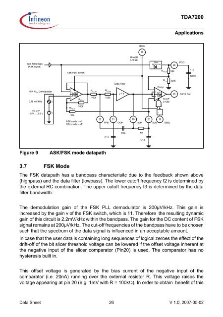
MSEL<br />
15<br />
from RSSI Gen<br />
(ASK signal)<br />
ASK/FSK Switch<br />
H=ASK<br />
L=FSK<br />
PEAK<br />
DETECTOR<br />
R T1 int<br />
26<br />
56k<br />
PDO<br />
C15<br />
100nF<br />
FSK PLL Demodulator<br />
0.18 mV/kHz<br />
typ. 2 V<br />
1.5 V......2.5 V<br />
AC DC<br />
+ - ASK<br />
+ FSK<br />
- R F3 int<br />
R F4 int<br />
30k<br />
300k<br />
R F1 int R F2 int<br />
v = 1<br />
100k<br />
100k<br />
Data Filter<br />
R T2<br />
390k<br />
Comp<br />
-<br />
+ CP<br />
25<br />
+ CM<br />
- H=CP<br />
L=CM<br />
DATA Out<br />
ASK mode: v=1<br />
FSK mode: v=11<br />
22 21<br />
19<br />
20<br />
FFB OOP<br />
SLP<br />
16<br />
SLN<br />
SSEL<br />
C12<br />
C14<br />
R1<br />
C13<br />
Figure 9<br />
ASK/FSK mode datapath<br />
3.7 FSK Mode<br />
The FSK datapath has a bandpass characterisitc due to the feedback shown above<br />
(highpass) and the data filter (lowpass). The lower cutoff frequency f2 is determined by<br />
the external RC-combination. The upper cutoff frequency f3 is determined by the data<br />
filter bandwidth.<br />
The demodulation gain of the FSK PLL demodulator is 200µV/kHz. This gain is<br />
increased by the gain v of the FSK switch, which is 11. Therefore the resulting dynamic<br />
gain of this circuit is 2.2mV/kHz within the bandpass. The gain for the DC content of FSK<br />
signal remains at 200µV/kHz. The cut-off frequencies of the bandpass have to be chosen<br />
such that the spectrum of the data signal is influenced in an acceptable amount.<br />
In case that the user data is containing long sequences of logical zeroes the effect of the<br />
drift-off of the bit slicer threshold voltage can be lowered if the offset voltage inherent at<br />
the negative input of the slicer comparator (Pin20) is used. The comparator has no<br />
hysteresis built in.<br />
This offset voltage is generated by the bias current of the negative input of the<br />
comparator (i.e. 20nA) running over the external resistor R. This voltage raises the<br />
voltage appearing at pin 20 (e.g. 1mV with R = 100kΩ). In order to obtain benefit of this<br />
Data Sheet 26 V 1.0, 2007-05-02