
You also want an ePaper? Increase the reach of your titles
YUMPU automatically turns print PDFs into web optimized ePapers that Google loves.
<strong>TDA7200</strong><br />
Functional Description<br />
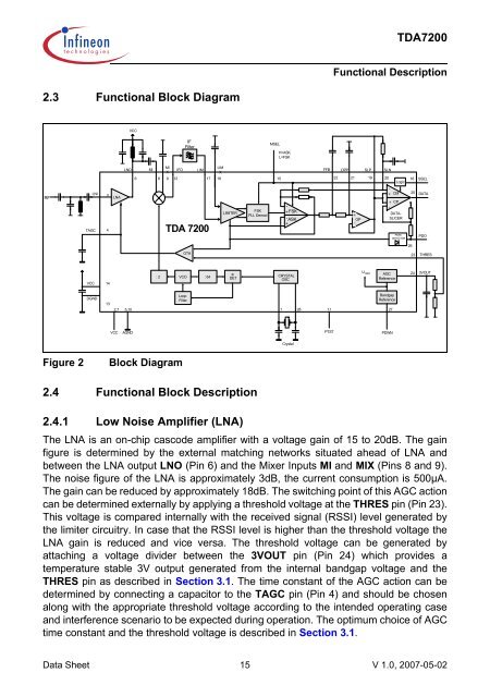
2.3 Functional Block Diagram<br />
VCC<br />
IF<br />
Filter<br />
MSEL<br />
H=ASK<br />
L=FSK<br />
RF<br />
TAGC<br />
VCC<br />
LNI<br />
3<br />
4<br />
14<br />
LNA<br />
MI<br />
LIM<br />
LNO MI IFO LIM<br />
FFB OPP<br />
X<br />
X<br />
6 8 9 12 17 18 15<br />
22 21 19 20<br />
TDA 7200<br />
OTA<br />
: 2 VCO : 64<br />
LIMITER<br />
Φ<br />
DET<br />
FSK<br />
PLL Demod<br />
-<br />
+ FSK<br />
-ASK<br />
+<br />
CRYSTAL<br />
OSC<br />
+<br />
-<br />
OP<br />
SLP<br />
SLN<br />
-<br />
+ CM<br />
AGC<br />
Reference<br />
Logic<br />
+ CP<br />
-<br />
DATA-<br />
SLICER<br />
PEAK<br />
DETECTOR<br />
U REF<br />
16<br />
25<br />
26<br />
23<br />
24<br />
SSEL<br />
DATA<br />
PDO<br />
THRES<br />
3VOUT<br />
DGND<br />
13<br />
Loop<br />
Filter<br />
Bandgap<br />
Reference<br />
2,7 5,10<br />
1 28 11<br />
27<br />
VCC<br />
AGND<br />
PTST<br />
PDWN<br />
Crystal<br />
Figure 2<br />
Block Diagram<br />
2.4 Functional Block Description<br />
2.4.1 Low Noise Amplifier (LNA)<br />
The LNA is an on-chip cascode amplifier with a voltage gain of 15 to 20dB. The gain<br />
figure is determined by the external matching networks situated ahead of LNA and<br />
between the LNA output LNO (Pin 6) and the Mixer Inputs MI and MIX (Pins 8 and 9).<br />
The noise figure of the LNA is approximately 3dB, the current consumption is 500µA.<br />
The gain can be reduced by approximately 18dB. The switching point of this AGC action<br />
can be determined externally by applying a threshold voltage at the THRES pin (Pin 23).<br />
This voltage is compared internally with the received signal (RSSI) level generated by<br />
the limiter circuitry. In case that the RSSI level is higher than the threshold voltage the<br />
LNA gain is reduced and vice versa. The threshold voltage can be generated by<br />
attaching a voltage divider between the 3VOUT pin (Pin 24) which provides a<br />
temperature stable 3V output generated from the internal bandgap voltage and the<br />
THRES pin as described in Section 3.1. The time constant of the AGC action can be<br />
determined by connecting a capacitor to the TAGC pin (Pin 4) and should be chosen<br />
along with the appropriate threshold voltage according to the intended operating case<br />
and interference scenario to be expected during operation. The optimum choice of AGC<br />
time constant and the threshold voltage is described in Section 3.1.<br />
Data Sheet 15 V 1.0, 2007-05-02