Novel of Normally-off GaN HEMT Device Structure by ... - CS Mantech
Novel of Normally-off GaN HEMT Device Structure by ... - CS Mantech
Novel of Normally-off GaN HEMT Device Structure by ... - CS Mantech

Create successful ePaper yourself
Turn your PDF publications into a flip-book with our unique Google optimized e-Paper software.
<strong>Novel</strong> <strong>of</strong> <strong>Normally</strong>-<strong>of</strong>f <strong>GaN</strong> <strong>HEMT</strong> <strong>Device</strong> <strong>Structure</strong> <strong>by</strong> Using Nano-rods Technology<br />
Chwan-Ying Lee, Young-Shying Chen , Lurng-Shehng Lee, Chien-Chung Hung, Cheng-Tyng Yen, Suh-<br />
Fang Lin, Rong Xuan, Wei-Hung Kuo, Tzu-Kun Ku, and Ming-Jinn Tsai<br />
Electronics and OptoElectronics Research Laboratories (EOL), ITRI<br />
No.195, Sec.4, Chung Hsing Rd., Chutung, Hsinchu, 31040, Taiwan, R.O.C.<br />
*Email: cyleei@itri.org.tw; Phone: +886-3-591-3490<br />
Keywords: <strong>GaN</strong> on Si, <strong>Normally</strong>-<strong>of</strong>f, nano-rod<br />
Abstract<br />
This paper reports a novel process <strong>by</strong> introducing<br />
nano-rods technique into Al<strong>GaN</strong>/<strong>GaN</strong> high-electronmobility-transistor<br />
(<strong>HEMT</strong>) device. This process adapts<br />
nickel to form the nano-rod hard mask pattern and then<br />
transfers to the electron supply Al<strong>GaN</strong> layer <strong>of</strong> the twodimensional<br />
electron gas (2DEG) device, followed <strong>by</strong> SF 6<br />
irradiation and p-<strong>GaN</strong> layer encapsulation. This device<br />
with the novel gate structure exhibits normally-<strong>of</strong>f<br />
characteristic. The threshold voltage <strong>of</strong> this nano-rod<br />
device is higher than 0.5V and the breakdown voltage is<br />
higher than 1500V.<br />
INTRODUCTION<br />
The High-Electron-Mobility Transistor (<strong>HEMT</strong>) device<br />
based on Al<strong>GaN</strong>/<strong>GaN</strong> hetero structure has low resistance<br />
characteristic <strong>by</strong> taking advantage <strong>of</strong> two-dimensional<br />
electron gas (2DEG) induced <strong>by</strong> piezoelectric polarization<br />
mechanism, so this device has been attracting considerable<br />
attention and intensively studied as for the next-generation<br />
power electronic devices. However, the conventional<br />
<strong>HEMT</strong> device typically has a negative threshold voltage<br />
because <strong>of</strong> the inherent existence <strong>of</strong> the 2DEG channel, and<br />
thus it becomes a normally-on device. This is rather<br />
inconvenient <strong>of</strong> use for some safety-concerned applications.<br />
Several techniques to achieve the normally-<strong>of</strong>f property <strong>of</strong><br />
the Al<strong>GaN</strong>/<strong>GaN</strong> devices have been reported, such as the<br />
fluoride-based plasma treatment method[1][2], the use <strong>of</strong> p-<br />
type layers underneath the gate region[3]-[5] to lift up the<br />
conduction band, or thin down the electron supply Al<strong>GaN</strong><br />
layer to form a recessed gate structure[6][7]. This recess<br />
would weaken the electric field contributed <strong>by</strong> a lower<br />
piezoelectric polarization, and generate a lower carrier<br />
concentraion in the 2DEG layer for Vt improvement.<br />
However, this approach is difficult to control the remaining<br />
Al<strong>GaN</strong> thickness and therefore exhibits poor device<br />
uniformity. Although many papers adopted various methods<br />
to achieve normally-<strong>of</strong>f property, it sacrificed device turn-on<br />
performance in some cases. The purpose <strong>of</strong> this study is to<br />
develop a normally-<strong>of</strong>f device with minimum impact on the<br />
drain current <strong>by</strong> proposing a novel imprint method to form<br />
the nano-rod or nano-strip gate structures.<br />
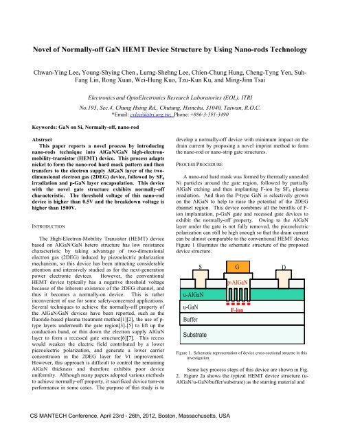
PROCESS PROCEDURE<br />
A nano-rod hard mask was formed <strong>by</strong> thermally annealed<br />
Ni particles around the gate region, followed <strong>by</strong> partially<br />
Al<strong>GaN</strong> etching and then implanting F-ion <strong>by</strong> SF 6 plasma<br />
irradiation. And then the P-type <strong>GaN</strong> is selectively grown<br />
on the Al<strong>GaN</strong> to help to raise the potential <strong>of</strong> the 2DEG<br />
channel region. This device combines all the benifits <strong>of</strong> F-<br />
ion implantation, p-<strong>GaN</strong> gate and recessed gate devices to<br />
exhibit the normally-<strong>of</strong>f property. Owing to the Al<strong>GaN</strong><br />
layer under the gate is not fully removed, the piezoelectric<br />
polarization can still be high enough so that the drain current<br />
can be almost comparable to the conventional <strong>HEMT</strong> device.<br />
Figure 1 illustrates the schematic structure <strong>of</strong> the proposed<br />
device structure.<br />
u-Al<strong>GaN</strong><br />
u-<strong>GaN</strong><br />
Buffer<br />
Substrate<br />
S G D<br />
p-Al<strong>GaN</strong><br />
F-ion<br />
Figure 1. Schematic representation <strong>of</strong> device cross-sectional structre in this<br />
investigation.<br />
Some key process steps <strong>of</strong> this device are shown in Fig.<br />
2. Figure 2a shows the typical <strong>HEMT</strong> device structure (u-<br />
Al<strong>GaN</strong>/u-<strong>GaN</strong>/buffer/substrate) as the starting material and<br />
<strong>CS</strong> MANTECH Conference, April 23rd - 26th, 2012, Boston, Massachusetts, USA
then deposits the oxide material as for the etching hard<br />
mask layer. Figure 2b shows the hard mask opening and the<br />
oxide<br />
u-Al<strong>GaN</strong><br />
u-<strong>GaN</strong><br />
Buffer<br />
Substrate<br />
(a)<br />
Nano-rod structure formed in the oxide layer <strong>by</strong> using<br />
imprint method. The nano-rod pattern was transferred into<br />
Al<strong>GaN</strong> layer and then the SiO 2 layer was removed as shown<br />
in Fig. 2c. Then, the F-ion was implanted <strong>by</strong> SF 6 plasma<br />
irradiation as shown in Fig. 2d, the thick oxide layer was<br />
used as hard mask. Last, the p-<strong>GaN</strong> layer was selectively<br />
grown on the gate region as shown in Fig. 2e. After that, the<br />
standard process <strong>of</strong> ohmic contact on the source and drain<br />
region (Fig. 2f) and Schottky contact on the gate region (Fig.<br />
2g) was performed.<br />
Substrate<br />
(b)<br />
Figure 3 shows the schematic representation <strong>of</strong> process<br />
steps <strong>of</strong> the imprint method. The Nickel material was<br />
deposited on SiO2 layer and then thermally annealed to form<br />
the nano-rod pattern around the gate region and then the<br />
oxide hard mark was formed <strong>by</strong> the ICP reactive ion etching.<br />
Substrate<br />
(c)<br />
SF 6<br />
oxide<br />
Ni<br />
SiO 2<br />
SiO 2<br />
1.6 mm <strong>GaN</strong> thick <strong>GaN</strong><br />
1.6 mm <strong>GaN</strong> thick <strong>GaN</strong><br />
<strong>GaN</strong><br />
<strong>GaN</strong><br />
Substrate<br />
(d)<br />
Sapphire substrate<br />
substrate<br />
Sapphire substrate<br />
substrate<br />
substrate<br />
substrate<br />
(a) <strong>GaN</strong> grown followed (b) Ni deposition. (c) Ni particle formed (d) SiO2 Nanorodsformed nano <strong>by</strong><br />
<strong>by</strong> SiO2 deposition <strong>by</strong> thermal annealing formed <strong>by</strong> ICP RIE.<br />
Figure 3. Schematic representation <strong>of</strong> Nano-rod formation.<br />
p-Al<strong>GaN</strong><br />
EXPERIMENTAL RESULTS<br />
Substrate<br />
S<br />
(e)<br />
D<br />
Figure 4 shows the tilt SEM view <strong>of</strong> one Ni nano-rod<br />
structure around gate region. The area ratio occupied <strong>by</strong><br />
these nano rods is about 38% . The threshold voltage and<br />
the output characteristic <strong>of</strong> this device can be adjusted <strong>by</strong><br />
designing different area ratio <strong>of</strong> the nano-rod structure. We<br />
believe the partially etched Al<strong>GaN</strong> layer, i.e. nano-rod<br />
structure, can has better trade<strong>of</strong>f characteristic as compared<br />
to the fully etched Al<strong>GaN</strong> layer, i.e. gate-recessed structure.<br />
And this result proves the feasibility <strong>of</strong> the proposed nanorod<br />
process.<br />
Substrate<br />
S<br />
(f)<br />
G<br />
D<br />
Substrate<br />
(g)<br />
Figure 2. Key process steps for the novel device.<br />
Figure 4. SEM view <strong>of</strong> Ni nano-rod structure.<br />
<strong>CS</strong> MANTECH Conference, April 23rd - 26th, 2012, Boston, Massachusetts, USA
Figure 5 shows a cross-sectional SEM image <strong>of</strong> the<br />
nano-rod structure after oxide hard mask opening. This<br />
nano-rod process is unlike the recessed-gate process, in<br />
which the whole area <strong>of</strong> Al<strong>GaN</strong> layer underneath the gate<br />
electrode is removed. The piezoelectric polarization may<br />
decrease too much from fully etched the Al<strong>GaN</strong> layer <strong>of</strong> the<br />
recessed-gate structure. So, the drain current is not easy to<br />
maintain a higher level. The etch process <strong>of</strong> the recessedgate<br />
process usually not easy to control and sometimes<br />
damages the 2DEG layer, and therefore contributes to nonuniformity<br />
<strong>of</strong> threshold voltage and decrease <strong>of</strong> drain current.<br />
As to the nano-rod structure, certain ratio <strong>of</strong> the 2DEG layer<br />
remains underneath the gate region, the device can have<br />
higher drain current as compared to the typical recessed-gate<br />
structure.<br />
The threshold voltage Vth can be extracted from the<br />
linear extrapolation <strong>of</strong> the Id-Vgs plot in Fig. 6. A positive<br />
Vth value <strong>of</strong> 1V was achieved from the nano-rod <strong>HEMT</strong><br />
device, while a negative value <strong>of</strong> -2V was presented from<br />
the standard Al<strong>GaN</strong>/<strong>GaN</strong> <strong>HEMT</strong> device.<br />
Figure 7 shows the reverse blocking characteristic <strong>of</strong><br />
the proposed nano-rod <strong>HEMT</strong> device. The breakdown<br />
voltage <strong>of</strong> this device is higher than 1500V. This is a good<br />
result that exhibits high current, normally <strong>of</strong>f, and large<br />
breakdown voltage at the same time <strong>by</strong> the novel nano-rod<br />
structure.<br />
Ni<br />
5000Å<br />
SiO 2<br />
rods<br />
<strong>GaN</strong> Template<br />
Figure 5. Crossectional SEM view <strong>of</strong> SiO2 nano-rod structure.<br />
Figure 6 shows the comparison <strong>of</strong> the DC transfer<br />
characteristics on different <strong>HEMT</strong> devices. The nano-rod<br />
device exhibits a peak drain current Id <strong>of</strong> 170 mA/mm at<br />
gate to source voltage Vgs <strong>of</strong> 5V. This value does not<br />
degrade too much as compared to peak Id <strong>of</strong> 220 mA/mm at<br />
Vgs <strong>of</strong> 4V from the standard <strong>HEMT</strong> device.<br />
Figure 7. Reverse blocking characteristic <strong>of</strong> the novel device.<br />
This is a preliminary result that shows good device<br />
properties on the on-state current, <strong>of</strong>f-state voltage, and gate<br />
control capability. However, we still need to optimize<br />
device performance and also simplify the nano-rod process.<br />
Figure 8. shows alternative approach <strong>by</strong> nano-imprint<br />
process, which can easily achieve different pattern density <strong>of</strong><br />
the nano-rods. The trade<strong>of</strong>f characteristics <strong>of</strong> on-state<br />
current and threshold voltage can therefore be optimized<br />
according to experiment <strong>by</strong> changing the nano-rod area ratio.<br />
Figure 8. Proposed a simplified nano-imprint process flow for nano-rod<br />
<strong>GaN</strong> device<br />
Figure 6. Comparison <strong>of</strong> DC transfer characteristics on different <strong>GaN</strong>-on-Si<br />
<strong>HEMT</strong> devices. The nano-rod device shows normally-<strong>of</strong>f property.<br />
From the nano-rod device, the on-state drain current can<br />
be improved and modulated <strong>by</strong> increasing the area ratio <strong>of</strong><br />
the nano-rods underneath the gate region. In addition, the<br />
threshold voltage can also be increased <strong>by</strong> adding the F-ion<br />
implantation and the P-<strong>GaN</strong> expitaxy layer to exhibit a<br />
normally-<strong>of</strong>f characteristic. The breakdown voltage can still<br />
<strong>CS</strong> MANTECH Conference, April 23rd - 26th, 2012, Boston, Massachusetts, USA
maintain high enough value due to the discontinued 2DEG<br />
layers formation <strong>by</strong> the nano-rod hard mask patterning. We<br />
will continue to develop and optimize the device property<br />
and target to achieve a nano-rod device with threshold<br />
voltage higher than 1.5V and drain current larger than 300<br />
mA/mm.<br />
CONCLUSIONS<br />
In conclusion, we have demonstrated a nano-rod<br />
Al<strong>GaN</strong>/<strong>GaN</strong> <strong>HEMT</strong> device with normally-<strong>of</strong>f, high on-state<br />
current and high breakdown voltage performances. The<br />
positive threshold voltage and high drain current<br />
performance is attributed to the nano-rod structure<br />
underneath the gate region because <strong>of</strong> the discontinued<br />
2DEG layers formed so that the high current maintained and<br />
the threshold voltage can be modulated <strong>by</strong> F- irradiation and<br />
adopt P-<strong>GaN</strong> layer. This device also exhibits high<br />
breakdown voltage and low leakage current. The nano-rod<br />
Al<strong>GaN</strong>/<strong>GaN</strong> device is very promising for the high current<br />
and high voltage motor drive applications.<br />
REFERENCES<br />
[1] H. Mizuno, et al., Phys. Stat. Sol. (c ), vol.4, no. 7, p.2732 , July, 2007.<br />
[2] Y.Cai et al., IEEE Electron <strong>Device</strong> vol. 53, no. 9, p. 2207, 2006.<br />
[3] N. Tsuyukuchi, et al., Jpn. J. Appl. Phys., vol.45, no.11, p.L-319, 2006.<br />
[4] Y.Uemoto, et al., IEEE Electron <strong>Device</strong> vol. 54, no.12, p.3393, 2007.<br />
[5] X.Hu, et al., Electron. Lett., vol.36, no.8, p.753, 2000.<br />
[6] C. Chen, et al., IEEE Electron <strong>Device</strong> Letters, vol. 32, no. 10, p. 373,<br />
2011.<br />
[7] R. Chu, et al., IEEE Electron <strong>Device</strong> Letters, vol. 32, no. 5, p. 632, 2011.<br />
ACRONYMS<br />
<strong>HEMT</strong>: High Electron Mobility Transistor<br />
<strong>CS</strong> MANTECH Conference, April 23rd - 26th, 2012, Boston, Massachusetts, USA