Develop A Trimless Voltage-Controlled Oscillator - Ladyada.net
Develop A Trimless Voltage-Controlled Oscillator - Ladyada.net
Develop A Trimless Voltage-Controlled Oscillator - Ladyada.net

You also want an ePaper? Increase the reach of your titles
YUMPU automatically turns print PDFs into web optimized ePapers that Google loves.
DESIGN FEATURE<br />
<strong>Trimless</strong> VCO<br />
2<br />
m 1 2 EQ T<br />
g / C C >> R / Q<br />
for a min imum 21 : ratio (31)<br />
V CC<br />
The phase noise can be found from:<br />
2 2<br />
n o<br />
2 2 2<br />
o o EQ o<br />
Phase noise = I × ( 1 / V )<br />
[ ]<br />
× ( f / 2Q ) × R /( f − f (32)<br />
where:<br />
f o = the frequency of oscillation,<br />
C VAR = the varactor capacitance,<br />
Q L = the inductor quality factor,<br />
Q T = the tank quality factor,<br />
R EQ = the equivalent tank parallel<br />
resistance,<br />
g m = the oscillator bipolar transistor<br />
transconductance,<br />
V 0 = the RMS tank voltage,<br />
C T = the total tank capacitance,<br />
C 0 = the varactor coupling capacitance,<br />
Q V = the effective varactor quality<br />
factor,<br />
R S = the varactor series resistance,<br />
I Q = the oscillator transistor bias<br />
current, and<br />
I n = the collector shot noise.<br />
One very useful method to view an<br />
oscillator circuit is as a “reflection<br />
amplifier.” This intuitive concept is<br />
described in a classic article by John<br />
Boyles 7 and in a paper by Esdale. 8<br />
The “reflection amplifier” method<br />
permits the engineer to use S-parameters<br />
for design and measurement of<br />
the oscillator. Working with S-<br />
parameters facilitates the modeling<br />
and measurement of the actual oscillator<br />
circuit and helps develop<br />
insight into the circuit’s performance<br />
and potential problems. 9<br />
The “reflection amplifier”<br />
approach basically models the oscillator<br />
as an active circuit with a resonant<br />
load and describes the stable<br />
oscillation point in terms of the relative<br />
impedances. If the active circuit<br />
input S-parameters are plotted as<br />
1/S 11 , then the values can be directly<br />
plotted on a Smith chart with the of<br />
the resonant load. A convenient<br />
aspect of plotting 1/S 11 is that the<br />
impedance of R and X for the active<br />
circuit can be read and multiplied by<br />
–1 to provide the correct values of the<br />
negative resistance and reactance.<br />
This method of plotting the<br />
impedances provides a graphical rep-<br />
B<br />
E<br />
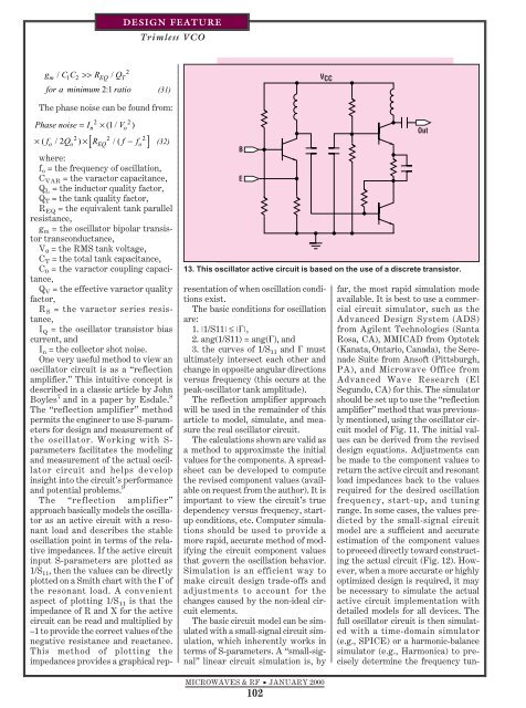
13. This oscillator active circuit is based on the use of a discrete transistor.<br />
resentation of when oscillation conditions<br />
exist.<br />
The basic conditions for oscillation<br />
are:<br />
1. 1/S11 ≤ ,<br />
2. ang(1/S11) = ang(), and<br />
3. the curves of 1/S 11 and must<br />
ultimately intersect each other and<br />
change in opposite angular directions<br />
versus frequency (this occurs at the<br />
peak-oscillator tank amplitude).<br />
The reflection amplifier approach<br />
will be used in the remainder of this<br />
article to model, simulate, and measure<br />
the real oscillator circuit.<br />
The calculations shown are valid as<br />
a method to approximate the initial<br />
values for the components. A spreadsheet<br />
can be developed to compute<br />
the revised component values (available<br />
on request from the author). It is<br />
important to view the circuit’s true<br />
dependency versus frequency, startup<br />
conditions, etc. Computer simulations<br />
should be used to provide a<br />
more rapid, accurate method of modifying<br />
the circuit component values<br />
that govern the oscillation behavior.<br />
Simulation is an efficient way to<br />
make circuit design trade-offs and<br />
adjustments to account for the<br />
changes caused by the non-ideal circuit<br />
elements.<br />
The basic circuit model can be simulated<br />
with a small-signal circuit simulation,<br />
which inherently works in<br />
terms of S-parameters. A “small-signal”<br />
linear circuit simulation is, by<br />
Out<br />
far, the most rapid simulation mode<br />
available. It is best to use a commercial<br />
circuit simulator, such as the<br />
Advanced Design System (ADS)<br />
from Agilent Technologies (Santa<br />
Rosa, CA), MMICAD from Optotek<br />
(Kanata, Ontario, Canada), the Serenade<br />
Suite from Ansoft (Pittsburgh,<br />
PA), and Microwave Office from<br />
Advanced Wave Research (El<br />
Segundo, CA) for this. The simulator<br />
should be set up to use the “reflection<br />
amplifier” method that was previously<br />
mentioned, using the oscillator circuit<br />
model of Fig. 11. The initial values<br />
can be derived from the revised<br />
design equations. Adjustments can<br />
be made to the component values to<br />
return the active circuit and resonant<br />
load impedances back to the values<br />
required for the desired oscillation<br />
frequency, start-up, and tuning<br />
range. In some cases, the values predicted<br />
by the small-signal circuit<br />
model are a sufficient and accurate<br />
estimation of the component values<br />
to proceed directly toward constructing<br />
the actual circuit (Fig. 12). However,<br />
when a more accurate or highly<br />
optimized design is required, it may<br />
be necessary to simulate the actual<br />
active circuit implementation with<br />
detailed models for all devices. The<br />
full oscillator circuit is then simulated<br />
with a time-domain simulator<br />
(e.g., SPICE) or a harmonic-balance<br />
simulator (e.g., Harmonica) to precisely<br />
determine the frequency tun-<br />
MICROWAVES & RF ■ JANUARY 2000<br />
102