Develop A Trimless Voltage-Controlled Oscillator - Ladyada.net
Develop A Trimless Voltage-Controlled Oscillator - Ladyada.net
Develop A Trimless Voltage-Controlled Oscillator - Ladyada.net

You also want an ePaper? Increase the reach of your titles
YUMPU automatically turns print PDFs into web optimized ePapers that Google loves.
DESIGN FEATURE<br />
<strong>Trimless</strong> VCO<br />
ing range and verify that<br />
the circuit design objectives<br />
can be met.<br />
EXAMPLE CIRCUIT<br />
Implementation of the<br />
Colpitts configuration<br />
shown in Fig. 7 is commonly<br />
accomplished with<br />
discrete transistors.<br />
Many options exist for<br />
cost-effective, high f T<br />
transistors packaged in<br />
small plastic packages—<br />
as single and dual<br />
devices. However, in<br />
order to achieve a design<br />
that works down to a<br />
+2.7-VDC supply voltage<br />
with sufficient headroom<br />
for the oscillator device<br />
and output buffer, a<br />
three-transistor circuit is<br />
typically needed. Figure<br />
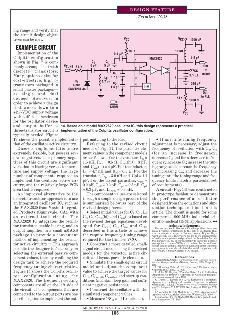
V CC<br />
10 <br />
C o C<br />
1<br />
c<br />
V TUNE 2 k 6 pF 5 pF<br />
2<br />
C 1<br />
L F 2.7 pF 3<br />
D 1<br />
4.7 nH<br />
C<br />
Alpha<br />
2<br />
4<br />
1.5 pF<br />
SMV1204-34<br />
SHDN<br />
0.1 F<br />
14. Based on a model MAX2620 oscillator IC, this design represents a practical<br />
implementation of the Colpitts oscillator configuration.<br />
Bias<br />
13 shows the possible implementation<br />
of the oscillator active circuitry.<br />
Discrete implementations are<br />
extremely flexible, but possess several<br />
negatives. The primary negatives<br />
of this circuit are significant<br />
variation in biasing versus temperature<br />
and supply voltage, the large<br />
number of components required to<br />
implement the oscillator active circuitry,<br />
and the relatively large PCB<br />
area that is required.<br />
An improved alternative to the<br />
discrete transistor approach is to use<br />
an integrated oscillator IC, such as<br />
the MAX2620 from Maxim Integrated<br />
Products (Sunnyvale, CA), with<br />
an external tank circuit. The<br />
MAX2620 IC integrates the oscillator<br />
transistor, stable biasing, and an<br />
output amplifier in a small uMAX8<br />
package to provide a convenient<br />
method of implementing the oscillator<br />
active circuitry. 10 This approach<br />
permits the designer to focus only on<br />
selecting the external passive component<br />
values, thereby confining the<br />
design task to achieve the required<br />
frequency tuning characteristics.<br />
Figure 14 shows the Colpitts oscillator<br />
configuration using the<br />
MAX2620. The frequency-setting<br />
components are all on the left side of<br />
the circuit. The components that are<br />
connected to the output ports are one<br />
possible option to implement the output<br />
matching to the load.<br />
Referring to the revised circuit<br />
model of Fig. 11, the parasitic-element<br />
values in the component models<br />
are as follows. For the varactor, L p =<br />
1.5 nH, R sv = 0.5 , C var (hi) = 8 pF,<br />
and C var (lo) = 4 pF. For the inductor,<br />
L p = 4.7 nH and R sl = 0.5 . For the<br />
transistor, L p ~ 3.0 nH and Cpi = 1.1<br />
pF. For the layout parasitics, C p1 =<br />
0.2 pF, C p2 = 0.2 pF, C p3 = 0.5 pF, C p4<br />
= 0.3 pF, and L trace = 0.3 nH.<br />
The component values are selected<br />
through a simple design process that<br />
is summarized below as part of the<br />
revised design process:<br />
• Select initial values for C 1 , C 2 , L f ,<br />
C c , C o , C var (hi), and C var (lo) based on<br />
the revised design equations developed<br />
for C var , C v , C in , and C 12e<br />
described in this article to achieve<br />
the require frequency tuning range<br />
required for the trimless VCO.<br />
• Construct a more detailed smallsignal<br />
circuit model using the revised<br />
models for the varactor, active circuit,<br />
and layout parasitic elements.<br />
• Simulate the small-signal circuit<br />
model and adjust the component<br />
value to achieve the target values for<br />
C in , C var(hi) , C var(lo) , and startup conditions<br />
(maintain loop gain and sufficient<br />
negative resistance).<br />
• Construct the oscillator with the<br />
simulated component values.<br />
• Measure 1/S 11 and (optional).<br />
MICROWAVES & RF ■ JANUARY 2000<br />
105<br />
MAX2620<br />
V CC<br />
V CC<br />
10 nH<br />
8<br />
7<br />
6<br />
5<br />
51 <br />
1000 pF<br />
1.5 pF<br />
V CC<br />
0.1 F<br />
330 pF<br />
1000 pF<br />
Out<br />
to<br />
mixer<br />
Out<br />
to PLL<br />
• If any fine-tuning frequency<br />
adjustment is necessary, adjust the<br />
frequency of oscillation with C o , C c<br />
(for an increase in frequency,<br />
decrease C c and for a decrease in frequency,<br />
increase C c ; increase the tuning<br />
range and decrease the frequency<br />
by increasing C o ; and decrease the<br />
tuning until the tuning range and frequency<br />
limits match a particular set<br />
of requirements).<br />
A circuit (Fig. 14) was constructed<br />
in prototype fashion to demonstrate<br />
the performance of an oscillator<br />
designed from the equations and simulation<br />
technique outlined in this<br />
article. The circuit is useful for some<br />
commercial 900-MHz industrial-scientific-medical<br />
(ISM) applications. ••<br />
Acknowledgments<br />
The author would like to acknowledge that there are<br />
many previous contributors to the field of oscillators that<br />
are the respected experts (Rohde, Leeson, Boyles, Hayward,<br />
Meyer, etc.). Their work has led to the advancement<br />
of oscillators in general and provided the foundation for this<br />
two-part article. My effort was simply to introduce a simple<br />
concept for a trimless VCO and to re-describe the oscillator<br />
design task in a simple, improved manner in order to permit<br />
an engineer to quickly calculate the initial component values<br />
for a PCB-based Colpitts VCO design.<br />
References<br />
5. Ken<strong>net</strong>h K. Clarke, Communications Circuits: Analysis<br />
and Design, Addison-Wesley, Boston, 1978, Chap. 6, p.<br />
225.<br />
6. “Modeling Coilcraft RF Inductors,” Technical Note,<br />
Coilcraft, Inc., Lisle, IL, 1999.<br />
7. John W. Boyles, “The <strong>Oscillator</strong> As A Reflection<br />
Amplifier: An Intuitive Approach To <strong>Oscillator</strong> Design,”<br />
Microwave Journal, June 1986.<br />
8. Daniel J. Esdale et al., “A Reflection Coefficient<br />
Approach to the Design of One-Port Negative Impedance<br />
<strong>Oscillator</strong>s,” IEEE Transactions on Microwave Theory<br />
and Techniques, Vol. MTT-29, No. 8, August 1981, pp. 770-<br />
776.<br />
9. “Varactor SPICE Models for RF VCO Applications,”<br />
Application Note, Alpha Industries, Woburn, MA, 1998.<br />
10. Datasheet for the MAX2620, Maxim Integrated Products,<br />
Sunnyvale, CA, 1997.