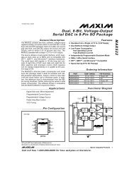
16-Bit Low Power Voltage Output w/I²C Interface Digital-to-Analog ...
16-Bit Low Power Voltage Output w/I²C Interface Digital-to-Analog ...
16-Bit Low Power Voltage Output w/I²C Interface Digital-to-Analog ...

You also want an ePaper? Increase the reach of your titles
YUMPU automatically turns print PDFs into web optimized ePapers that Google loves.
www.ti.com<br />
V REF<br />
3 mm x 5 mm<br />
DAC8571<br />
SLAS373A–DECEMBER 2002–REVISED JULY 2003<br />
<strong>16</strong>-BIT, LOW POWER, VOLTAGE OUTPUT, I 2 C INTERFACE DIGITAL-TO-ANALOG<br />
CONVERTER<br />
FEATURES<br />
DESCRIPTION<br />
• Micropower Operation: <strong>16</strong>0 µA @ 5 V The DAC8571 is a small low-power, <strong>16</strong>-bit voltage<br />
• <strong>Power</strong>-On Reset <strong>to</strong> Zero output DAC with an I 2 C compatible two-wire serial<br />
• Single Supply: +2.7 V <strong>to</strong> +5.5 V<br />
interface. Its on-chip precision output amplifier allows<br />
• <strong>16</strong>-<strong>Bit</strong> Mono<strong>to</strong>nic<br />
rail-<strong>to</strong>-rail output swing and settles within 10<br />
microseconds. The DAC8571 architecture is <strong>16</strong>-bit<br />
• Settling Time: 10 µs <strong>to</strong> ±0.003% FSR mono<strong>to</strong>nic, and fac<strong>to</strong>ry trimming typically achieves ±4<br />
• I 2 C <strong>Interface</strong> With High-Speed Mode mV absolute accuracy at all codes. The DAC8571<br />
• Supports Data Receive and Transmit<br />
requires an external reference voltage <strong>to</strong> set its output<br />
• On-Chip Rail-<strong>to</strong>-Rail <strong>Output</strong> Buffer<br />
voltage range.<br />
• Double-Buffered Input Register The low power consumption and small size of this part<br />
• Supports Synchronous Multichannel Update make it ideally suited <strong>to</strong> portable battery operated<br />
• Offset Error: ±1 mV max at 25°C<br />
equipment. The power consumption is typically 800 µW<br />
at V DD = 5 V reducing <strong>to</strong> 1 µW in power-down mode.<br />
• Full-Scale Error: ±3 mV max at 25°C<br />
• Small 8 Lead MSOP Package<br />
The DAC8571 incorporates a 2-wire I 2 C interface.<br />
Standard, fast, and high-speed modes of I 2 C operation<br />
are all supported up <strong>to</strong> 3.4 MHz serial clock speeds.<br />
APPLICATIONS<br />
Multichannel synchronous data update and<br />
• Process Control power-down operations are supported through the I 2 C<br />
• Data Acquisition Systems<br />
bus. DAC8571 is also capable of transmitting the con-<br />
• Closed-Loop Servo Control<br />
tents of its serial shift register, a key feature for I 2 C<br />
system verification.<br />
• PC Peripherals<br />
• Portable Instrumentation<br />
The DAC8571 is available in an 8-lead MSOP package<br />
and is specified over -40°C <strong>to</strong> 105°C.<br />
Ref +<br />
<strong>16</strong> <strong>Bit</strong> DAC<br />
_<br />
+<br />
V (SENSE)<br />
V OUT<br />
V DD<br />
<strong>16</strong><br />
DAC Register<br />
Temporary Register<br />
SDA<br />
SCL<br />
A0<br />
I 2 C Block<br />
<strong>Power</strong> Down<br />
Control Logic<br />
Resis<strong>to</strong>r<br />
Network<br />
GND<br />
I2C is a trademark of Philips Corporation.<br />
Please be aware that an important notice concerning availability, standard warranty, and use in critical applications of Texas Instruments<br />
semiconduc<strong>to</strong>r products and disclaimers there<strong>to</strong> appears at the end of this data sheet.<br />
PRODUCTION DATA information is current as of publication date.<br />
Products conform <strong>to</strong> specifications per the terms of Texas Instruments<br />
standard warranty. Production processing does not necessarily includetestingofallparameters.<br />
Copyright © 2002–2003, Texas Instruments Incorporated
DAC8571<br />
SLAS373A–DECEMBER 2002–REVISED JULY 2003<br />
www.ti.com<br />
V DD<br />
V REF<br />
V (SENSE)<br />
V OUT<br />
PIN CONFIGURATIONS<br />
1<br />
2<br />
3<br />
4<br />
8<br />
7<br />
6<br />
5<br />
GND<br />
SDA<br />
SCL<br />
A0<br />
PIN DESCRIPTION<br />
Pin Name Function<br />
1 V DD <strong>Analog</strong> voltage supply input<br />
2 V REF Positive reference voltage input<br />
3 V (SENSE) <strong>Analog</strong> output sense<br />
4 V OUT <strong>Analog</strong> output voltage from DAC<br />
5 A0 Device address select<br />
6 SCL Serial clock input<br />
7 SDA Serial data input/output<br />
8 GND Ground reference point for all circuitry on the part<br />
2
www.ti.com<br />
DAC8571<br />
SLAS373A–DECEMBER 2002–REVISED JULY 2003<br />
These devices have limited built-in ESD protection. The leads should be shorted <strong>to</strong>gether or the device placed in conductive foam<br />
during s<strong>to</strong>rage or handling <strong>to</strong> prevent electrostatic damage <strong>to</strong> the MOS gates.<br />
PACKAGE/ORDERING INFORMATION<br />
Product Package Package Desig- Specified Temperature Package Ordering Number Transport Mena<strong>to</strong>r<br />
Range Marking dia, Quantity<br />
DAC8571 8-MSOP DGK -40°C <strong>to</strong> +105°C D871 DAC8571IDGK Tube, 80<br />
DAC8571IDGKR Tape & Reel,<br />
2500<br />
ABSOLUTE MAXIMUM RATINGS (1)<br />
V DD <strong>to</strong> GND<br />
DAC8571<br />
-0.3 V <strong>to</strong> +6 V<br />
<strong>Digital</strong> input voltage <strong>to</strong> GND -0.3V <strong>to</strong> V DD + 0.3V<br />
V OUT <strong>to</strong> GND -0.3V <strong>to</strong> +V DD + 0.3V<br />
Operating temperature range -40°C <strong>to</strong> + 105°C<br />
S<strong>to</strong>rage temperature range<br />
-65°C <strong>to</strong> +150°C<br />
Junction temperature range (T J max) + 150°C<br />
Θ JA Thermal impedance<br />
Θ JC Thermal impedance<br />
260°C/W<br />
44°C/W<br />
Lead temperature, soldering Vapor phase 215°C<br />
(60s)<br />
Infrared (15s) 220°C<br />
(1) Stresses above those listed under “Absolute Maximum Ratings” may cause permanent damage <strong>to</strong> the device. Exposure <strong>to</strong> absolute<br />
maximum conditions for extended periods may affect device reliability.<br />
ELECTRICAL CHARACTERISTICS<br />
V DD = +2.7 V <strong>to</strong> +5.5 V; R L = 2 kΩ <strong>to</strong> GND; C L = 200 pF <strong>to</strong> GND; low power mode; all specifications -40°C <strong>to</strong> 105°C (unless<br />
otherwise noted)<br />
DAC8571<br />
PARAMETER CONDITIONS MIN TYP MAX UNITS<br />
STATIC PERFORMANCE (1)<br />
Resolution <strong>16</strong> <strong>Bit</strong>s<br />
Relative accuracy ±0.098 % of FSR<br />
Differential nonlinearity Mono<strong>to</strong>nic by design ±0.25 ±1 LSB<br />
Offset error Measured at code 485, 25°C 0.3 ±1.0 mV<br />
Measured at code 485, -40°C...105°C 1.0 ±5.0<br />
Full-scale error Measured at code 64714, 25°C 0.5 ±3.0 mV<br />
Measured at code 64714, -40°C...105°C 1.0 ±5.0<br />
Gain error Measured at code 64714, 25°C 1.0 ±3.0 mV<br />
Measured at code 64714, -40°C...105°C 2.0 ±5.0<br />
Zero code error drift All zeroes loaded <strong>to</strong> DAC register -20 µV/°C<br />
Gain temperature coefficient -5 ppm of FSR/°C<br />
Absolute accuracy All codes from code 485 <strong>to</strong> code 64714, 25°C ±2.5 mV<br />
All codes from code 485 <strong>to</strong> code 64714, ±3.5<br />
-40°C...105°C<br />
(1) Linearity calculated using a reduced code range of 485 <strong>to</strong> 64714. <strong>Output</strong> unloaded.<br />
3
DAC8571<br />
SLAS373A–DECEMBER 2002–REVISED JULY 2003<br />
www.ti.com<br />
ELECTRICAL CHARACTERISTICS (continued)<br />
V DD = +2.7 V <strong>to</strong> +5.5 V; R L = 2 kΩ <strong>to</strong> GND; C L = 200 pF <strong>to</strong> GND; low power mode; all specifications -40°C <strong>to</strong> 105°C (unless<br />
otherwise noted)<br />
DAC8571<br />
PARAMETER CONDITIONS MIN TYP MAX UNITS<br />
OUTPUT CHARACTERISTICS (2)<br />
<strong>Output</strong> voltage range 0 V REF V<br />
<strong>Output</strong> voltage settling time (full R L = 2 kΩ; C L < 200 pF, fast settling 8 10 µs<br />
scale)<br />
R L = 2 kΩ; C L = 500 pF, fast settling 12 µs<br />
R L = 2 kΩ; C L < 200 pF, low power 13 15 µs<br />
Slew rate R L = 2 kΩ; C L < 200 pF, fast settling 1 V/µs<br />
R L = 2 kΩ; C L < 200 pF, low power 0.5<br />
Capacitive load stability R L = ∞ 470 pF<br />
R L = 2 kΩ 1000 pF<br />
<strong>Digital</strong>-<strong>to</strong>-analog glitch impulse 20 nV-s<br />
<strong>Digital</strong> feedthrough 0.5 nV-s<br />
DC output impedance 1 Ω<br />
Short circuit current V DD = +5 V 50 mA<br />
V DD = +3 V 20 mA<br />
<strong>Power</strong>-up time Coming out of power-down mode, V DD = +5 V 2.5 µs<br />
Coming out of power-down mode, V DD = +3 V 5 µs<br />
PSRR 0.75 mV/V<br />
REFERENCE INPUT<br />
V REFH input range 0 V DD V<br />
Reference input impedance 140 kΩ<br />
LOGIC INPUTS (3)<br />
Input current ±1 µA<br />
V IN_L , Input low voltage V DD = 2.7-5.5 V 0.3V DD V<br />
V IN_H0 , Input high voltage V DD = 2.7-5.5 V 0.7V DD V<br />
Pin capacitance 3 pF<br />
POWER REQUIREMENTS<br />
V DD 2.7 5.5 V<br />
I DD (normal operation)<br />
DAC active, I ref included<br />
V DD = +4.5 V <strong>to</strong> +5.5 V V IH = V DD , V IL = GND, fast settling 250 400 µA<br />
V IH = V DD , V IL = GND, low power <strong>16</strong>0 225<br />
V DD = +2.7 V <strong>to</strong> +3.6 V V IH = V DD , V IL = GND, fast settling 240 380 µA<br />
I DD (all power-down modes)<br />
V IH = V DD , V IL = GND, low power 140 200<br />
DAC active, I ref included<br />
V DD = +4.5 V <strong>to</strong> +5.5 V V IH = V DD and V IL = GND 0.2 1 µA<br />
V DD = +2.7 V <strong>to</strong> +3.6 V V IH = V DD and V IL = GND 0.05 1 µA<br />
POWER EFFICIENCY<br />
I OUT /I DD I L = 2 mA, V DD = +5 V 93%<br />
(2) Assured by design and characterization, not production tested.<br />
(3) Assured by design and characterization, not production tested.<br />
4
www.ti.com<br />
DAC8571<br />
SLAS373A–DECEMBER 2002–REVISED JULY 2003<br />
TIMING CHARACTERISTICS<br />
V DD = +2.7 V <strong>to</strong> +5.5 V; R L = 2 kΩ <strong>to</strong> GND; all specifications -40°C <strong>to</strong> 105°C (unless otherwise noted)<br />
SYMBOL PARAMETER TEST CONDITIONS MIN TYP MAX UNITS<br />
t SCL<br />
SCL clock frequency<br />
Standard mode 100 kHz<br />
Fast mode 400 kHz<br />
High-speed mode, C B - 100pF max 3.4 MHz<br />
High-speed mode, C B - 400pF max 1.7 MHz<br />
Bus free time between a STOP and<br />
Standard mode 4.7 µs<br />
t BUF START condition Fast mode 1.3 µs<br />
Standard mode 4.0 \µs<br />
t HO ; t STA<br />
Hold time (repeated) START con-<br />
dition<br />
Fast mode 600 ns<br />
High-speed mode <strong>16</strong>0 ns<br />
t LOW<br />
t HIGH<br />
LOW period of the SCL clock<br />
HIGH period of the SCL clock<br />
Standard mode 4.7 µs<br />
Fast mode 1.3 µs<br />
Standard mode 4.0 µs<br />
Fast mode 600 ns<br />
High-speed mode, C B - 100pF max 60 ns<br />
High-speed mode, C B - 400pF max 120 ns<br />
Standard mode 4.7 µs<br />
t SU ; t STA<br />
Setup time for a repeated START<br />
condition<br />
Fast mode 600 ns<br />
High-speed mode <strong>16</strong>0 ns<br />
Standard mode 250 ns<br />
t SU ; t DAT Data setup time Fast mode 100 ns<br />
t HD ; t DAT<br />
t RCL<br />
t RCL1<br />
t FCL<br />
t RCA<br />
t FDA<br />
Data hold time<br />
Rise time of SCL signal<br />
High-speed mode 10 ns<br />
Standard mode 0 0.9 µs<br />
Fast mode 0 0.9 µs<br />
High-speed mode, C B - 100pF max 0 70 ns<br />
High-speed mode, C B - 400pF max 0 150 ns<br />
Standard mode 20 × 0.1C B 1000 ns<br />
Fast mode 20 × 0.1C B 300 ns<br />
High-speed mode, C B - 100pF max 10 40 ns<br />
High-speed mode, C B - 400pF max 20 80 ns<br />
Standard mode 20 × 0.1C B 1000 ns<br />
Rise time of SCL signal after a Fast mode 20 × 0.1C B 300 ns<br />
repeated START condition, and<br />
after an acknowledge BIT High-speed mode, C B - 100pF max 10 80 ns<br />
High-speed mode, C B - 400pF max 20 <strong>16</strong>00 ns<br />
Fall time of SCL signal<br />
Rise time of SDA signal<br />
Fall time of SDA signal<br />
Standard mode 20 × 0.1C B 300 ns<br />
Fast mode 20 × 0.1C B 300 ns<br />
High-speed mode, C B - 100pF max 10 40 ns<br />
High-speed mode, C B - 400pF max 20 80 ns<br />
Standard mode 20 × 0.1C B 1000 ns<br />
Fast mode 20 × 0.1C B 300 ns<br />
High-speed mode, C B - 100pF max 10 80 ns<br />
High-speed mode, C B - 400pF max 20 <strong>16</strong>0 ns<br />
Standard mode 20 × 0.1C B 300 ns<br />
Fast mode 20 × 0.1C B 300 ns<br />
High-speed mode, C B - 100pF max 10 80 ns<br />
High-speed mode, C B - 400pF max 20 <strong>16</strong>0 ns<br />
5
DAC8571<br />
SLAS373A–DECEMBER 2002–REVISED JULY 2003<br />
www.ti.com<br />
TIMING CHARACTERISTICS (continued)<br />
V DD = +2.7 V <strong>to</strong> +5.5 V; R L = 2 kΩ <strong>to</strong> GND; all specifications -40°C <strong>to</strong> 105°C (unless otherwise noted)<br />
SYMBOL PARAMETER TEST CONDITIONS MIN TYP MAX UNITS<br />
Standard mode 4.0 µs<br />
t SU ; t STO Setup time for STOP condition Fast mode 600 ns<br />
High-speed mode <strong>16</strong>0 ns<br />
C B Capacitive load for SDA and SCL 400 pF<br />
t SP<br />
Pulse width of spike suppressed<br />
Fast mode 50 ns<br />
High-speed mode 10 ns<br />
Noise margin at the HIGH level for<br />
Standard mode<br />
V NH each connected device (including Fast mode 0.2V DO V<br />
hysteresis)<br />
High-speed mode<br />
Noise margin at the LOW level for<br />
Standard mode<br />
V NL each connected device (including Fast mode 0.1V DO V<br />
hysteresis)<br />
High-speed mode<br />
6
www.ti.com<br />
DAC8571<br />
SLAS373A–DECEMBER 2002–REVISED JULY 2003<br />
Linearity Error - LSB<br />
LINEARITY ERROR vs DIGITAL INPUT CODE<br />
64<br />
48<br />
32<br />
<strong>16</strong><br />
0<br />
-<strong>16</strong><br />
-32<br />
-48<br />
-64<br />
0 10000 20000 30000 40000 50000 60000<br />
TYPICAL CHARACTERISTICS<br />
At T A = +25°C, unless otherwise noted.<br />
DLE - LSB<br />
DIFFERENTIAL LINEARITY ERROR vs DIGITAL INPUT<br />
CODE<br />
1<br />
0.8<br />
0.6<br />
0.4<br />
0.2<br />
0<br />
-0.2<br />
-0.4<br />
-0.6<br />
-0.8<br />
-1<br />
0 10000 20000 30000 40000 50000 60000<br />
<strong>Digital</strong> Input Code<br />
<strong>Digital</strong> Input Code<br />
Figure 1. Figure 2.<br />
3<br />
ERROR vs TEMPERATURE<br />
3<br />
ERROR vs TEMPERATURE<br />
2<br />
Full–Scale<br />
V DD = 5 V<br />
2<br />
V DD = 3 V<br />
Error – mV<br />
1<br />
0<br />
–1<br />
Gain<br />
Zero–Scale<br />
Error – mV<br />
1<br />
0<br />
–1<br />
Gain<br />
Zero–Scale<br />
Full–Scale<br />
–2<br />
–2<br />
–3<br />
–3<br />
–40 –20 0 20 40 60 80 100<br />
–40 –20 0 20 40 60 80 100<br />
T A – Free–Air Temperature – °C<br />
T A – Free–Air Temperature – °C<br />
Figure 3. Figure 4.<br />
Linearity Error - LSB<br />
64<br />
48<br />
32<br />
<strong>16</strong><br />
0<br />
-<strong>16</strong><br />
-32<br />
-48<br />
LINEARITY ERROR<br />
vs<br />
TEMPERATURE<br />
MAX Error<br />
MIN Error<br />
-64<br />
-40 0 40 80 110<br />
T A - Free-Air Temperature - °C<br />
Differential Linearity Error - LSB<br />
1<br />
0.8<br />
0.6<br />
0.4<br />
0.2<br />
0<br />
-0.2<br />
-0.4<br />
-0.6<br />
-0.8<br />
DIFFERENTIAL LINEARITY ERROR<br />
vs<br />
TEMPERATURE<br />
MAX Error<br />
MIN Error<br />
-1<br />
-40 0 40 80 110<br />
T A - Free-Air Temperature - °C<br />
Figure 5. Figure 6.<br />
7
DAC8571<br />
SLAS373A–DECEMBER 2002–REVISED JULY 2003<br />
www.ti.com<br />
TYPICAL CHARACTERISTICS (continued)<br />
At T A = +25°C, unless otherwise noted.<br />
0.15<br />
SINK CURRENT AT NEGATIVE RAIL<br />
5<br />
SOURCE CURRENT AT POSITIVE RAIL<br />
VOUT - <strong>Output</strong> <strong>Voltage</strong> - V<br />
0.125<br />
0.1<br />
0.075<br />
0.05<br />
0.025<br />
0<br />
V DD = 2.7 V<br />
V REF = V DD - 10 mV<br />
V DD = 5 V<br />
DAC Loaded With 0000 H<br />
0 1 2 3 4 5<br />
VOUT - <strong>Output</strong> <strong>Voltage</strong> - V<br />
I SINK - Sink Current - mA<br />
I SOURCE - Source Current - mA<br />
Figure 7. Figure 8.<br />
4.95<br />
4.9<br />
4.85<br />
4.8<br />
V REF = V DD - 10 mV<br />
DAC Loaded With FFFF H<br />
V DD = 5 V<br />
0 1 2 3 4 5<br />
2.7<br />
SOURCE CURRENT AT POSITIVE RAIL<br />
SUPPLY CURRENT vs DIGITAL INPUT CODE<br />
250<br />
VOUT - <strong>Output</strong> <strong>Voltage</strong> - V<br />
2.65<br />
2.6<br />
2.55<br />
2.5<br />
V REF = V DD - 10 mV<br />
DAC Loaded With FFFF H<br />
V DD = 2.7 V<br />
0 1 2 3 4 5<br />
I SOURCE - Source Current - mA<br />
IDD - Supply Current - µA<br />
200<br />
150<br />
100<br />
50<br />
0<br />
V DD = 5 V<br />
Reference Current Included<br />
V DD = 3.6 V<br />
0 10000 20000 30000 40000 50000 60000<br />
<strong>Digital</strong> Input Code<br />
Figure 9. Figure 10.<br />
I DD – Supply Current – µA<br />
250<br />
200<br />
150<br />
100<br />
50<br />
SUPPLY CURRENT vs TEMPERATURE<br />
I REF Included<br />
V DD = 5.5 V<br />
V DD = 3.6 V<br />
IDD - Supply Current - µA<br />
140<br />
120<br />
100<br />
80<br />
60<br />
40<br />
20<br />
SUPPLY CURRENT vs SUPPLY VOLTAGE<br />
V REF = V DD , I DD Measured at <strong>Power</strong>-Up,<br />
Reference Current Included, No Load<br />
0<br />
0<br />
–40 –20 0 20 40 60 80 100<br />
2.7 3.1 3.5 3.9 4.3 4.7 5.1 5.5<br />
T A – Free–Air Temperature – °C<br />
V DD - Supply <strong>Voltage</strong> - V<br />
Figure 11. Figure 12.<br />
8
www.ti.com<br />
DAC8571<br />
SLAS373A–DECEMBER 2002–REVISED JULY 2003<br />
TYPICAL CHARACTERISTICS (continued)<br />
At T A = +25°C, unless otherwise noted.<br />
IDD - Supply Current - mA<br />
SUPPLY CURRENT vs LOGIC INPUT VOLTAGE<br />
1<br />
T<br />
0.9 A = 25°C, A0 Input (All Other Inputs = GND)<br />
Reference Current Included<br />
0.8<br />
0.7<br />
0.6<br />
0.5<br />
0.4<br />
0.3<br />
0.2<br />
0.1<br />
0<br />
V DD = V REF = 5.5 V<br />
V DD = V REF = 2.7 V<br />
0 1 2 3 4 5<br />
f - Frequency<br />
2500<br />
2000<br />
1500<br />
1000<br />
500<br />
0<br />
HISTOGRAM OF CURRENT CONSUMPTION<br />
I REF Included<br />
V DD = 2.7 V<br />
V DD = 5.5 V<br />
0 40 80 120 <strong>16</strong>0 200 240 280<br />
Logic Input <strong>Voltage</strong> - V<br />
I DD - Supply Current - µA<br />
Figure 13. Figure 14.<br />
VOUT - <strong>Output</strong> <strong>Voltage</strong> - V<br />
5.5<br />
5<br />
4.5<br />
4<br />
3.5<br />
3<br />
2.5<br />
2<br />
1.5<br />
1<br />
0.5<br />
0<br />
-0.5<br />
EXITING POWER-DOWN MODE<br />
V O<br />
(V, 50 mV/div)<br />
2.5<br />
2.45<br />
2.4<br />
2.35<br />
OUTPUT GLITCH (Mid-Scale)<br />
V ref = V DD - 50 mV<br />
Code 7FFFh <strong>to</strong> 8000h<br />
(Glitch Occurs Every N x 4096<br />
Code Boundary)<br />
2.3<br />
t - Time - 5µs/div<br />
0 5 10 15 20 25 30<br />
t - Time - µS<br />
Figure 15. Figure <strong>16</strong>.<br />
Total Unadjusted Error - V<br />
0.005<br />
0.004<br />
0.003<br />
0.002<br />
0.001<br />
0<br />
-0.001<br />
-0.002<br />
-0.003<br />
-0.004<br />
-0.005<br />
V DD = 5 V<br />
ABSOLUTE ERROR<br />
0 10000 20000 30000 40000 50000 60000<br />
V OUT – <strong>Output</strong> <strong>Voltage</strong> – V<br />
FULL-SCALE SETTLING TIME (Large Signal)<br />
6<br />
5<br />
4<br />
3<br />
2<br />
1<br />
0<br />
V DD = V REF<br />
= 5 V<br />
<strong>Output</strong><br />
Loaded With<br />
2 kΩ and<br />
200 pF <strong>to</strong><br />
GND<br />
t – Time – 12µs/div, Fast–Settling Mode<br />
<strong>Digital</strong> Input Code<br />
Figure 17. Figure 18.<br />
9
DAC8571<br />
SLAS373A–DECEMBER 2002–REVISED JULY 2003<br />
www.ti.com<br />
TYPICAL CHARACTERISTICS (continued)<br />
At T A = +25°C, unless otherwise noted.<br />
HALF-SCALE SETTLING TIME (Large Signal)<br />
3.0<br />
FULL-SCALE SETTLING TIME (Large Signal)<br />
3.5<br />
V OUT – <strong>Output</strong> <strong>Voltage</strong> – V<br />
2.5<br />
2.0<br />
1.5<br />
1.0<br />
0.5<br />
0.0<br />
V DD = V REF<br />
= 5 V<br />
<strong>Output</strong><br />
Loaded With<br />
2 kΩ and<br />
200 pF <strong>to</strong><br />
GND<br />
V OUT – <strong>Output</strong> <strong>Voltage</strong> – V<br />
3.0<br />
2.5<br />
2.0<br />
1.5<br />
1.0<br />
0.5<br />
0.0<br />
V DD = V REF<br />
= 2.7 V<br />
<strong>Output</strong><br />
Loaded With<br />
2 kΩ and<br />
200 pF <strong>to</strong><br />
GND<br />
t – Time – 12µs/div, Fast–Settling Mode<br />
t – Time – 12µs/div, Fast–Settling Mode<br />
Figure 19. Figure 20.<br />
HALF-SCALE SETTLING TIME<br />
SIGNAL-TO-NOISE RATIO vs vs OUTPUT FREQUENCY FREQUENCY<br />
98<br />
V OUT – <strong>Output</strong> <strong>Voltage</strong> – V<br />
1.50<br />
1.00<br />
0.50<br />
0.00<br />
V DD = V REF<br />
= 2.7 V<br />
<strong>Output</strong><br />
Loaded With<br />
2 kΩ and<br />
200 pF <strong>to</strong><br />
GND<br />
t – Time – 12µs/div, Fast–Settling Mode<br />
SNR (dB)<br />
96<br />
94<br />
92<br />
90<br />
V DD = 2.7V<br />
V DD = 5V<br />
88<br />
V DD = V REF<br />
86 -1dB FSR <strong>Digital</strong> Input, F S = 52ksps<br />
Measurement Bandwidth = 20kHz<br />
84<br />
0 500 1k 1.5k 2k 2.5k 3k 3.5k 4k 4.5k<br />
<strong>Output</strong> Frequency (Hz), Fast-Settling Mode<br />
Figure 21. Figure 22.<br />
THD (dB)<br />
TOTAL HARMONIC DISTORTION vs OUTPUT FRE-<br />
OUTPUT QUENCY FREQUENCY<br />
0<br />
- 10 V DD = V REF = 5V<br />
F S = 52ksps, - 1dB FSR <strong>Digital</strong> Input<br />
- 20 Measurement Bandwidth = 20kHz<br />
- 30<br />
- 40<br />
- 50<br />
- 60<br />
- 70<br />
THD<br />
- 80<br />
-80<br />
3rd Harmonic<br />
- 90<br />
-90<br />
2nd Harmonic<br />
- 100<br />
-100<br />
2nd Harmonic<br />
3rd Harmonic<br />
0 500 1k 1.5k 2k 2.5k 3k 3.5k 4k<br />
0 500 1k 1.5k 2k 2.5k 3k 3.5k 4k<br />
<strong>Output</strong> Frequency (Hz), Fast-Settling Mode<br />
<strong>Output</strong> Frequency (Hz), Fast-Settling Mode<br />
Figure 23. Figure 24.<br />
THD (dB)<br />
TOTAL HARMONIC DISTORTION vs OUTPUT FRE-<br />
QUENCY<br />
0<br />
-10 V DD = V REF = 2.7V<br />
F S = 52ksps, -1dB FSR <strong>Digital</strong> Input<br />
-20 Measurement Bandwidth = 20kHz<br />
-30<br />
-40<br />
-50<br />
-60<br />
-70<br />
THD<br />
10
www.ti.com<br />
DAC8571<br />
SLAS373A–DECEMBER 2002–REVISED JULY 2003<br />
TYPICAL CHARACTERISTICS (continued)<br />
At T A = +25°C, unless otherwise noted.<br />
FULL-SCALE SETTLING TIME<br />
(Small-Signal-Positive Going Step)<br />
FULL-SCALE SETTLING TIME<br />
(Small-Signal-Negative Going Step)<br />
<strong>Output</strong> <strong>Voltage</strong><br />
Small-Signal Settling<br />
Time<br />
5mV/div<br />
<strong>Output</strong> <strong>Voltage</strong><br />
Small-Signal Settling<br />
Time<br />
5mV/div<br />
Trigger<br />
Signal<br />
Trigger<br />
Signal<br />
Time (2µs/div)<br />
Time (2µs/div)<br />
Figure 25. Figure 26.<br />
11
DAC8571<br />
SLAS373A–DECEMBER 2002–REVISED JULY 2003<br />
www.ti.com<br />
D/A SECTION<br />
THEORY OF OPERATION<br />
The architecture of the DAC8571 consists of a string DAC followed by an output buffer amplifier. Figure 27<br />
shows a block diagram of the DAC architecture.<br />
Reference <strong>Voltage</strong><br />
DAC Register<br />
Ref+<br />
Resis<strong>to</strong>r<br />
String<br />
Ref-<br />
_<br />
+<br />
V (SENSE)<br />
V OUT<br />
GND<br />
Figure 27. DAC8571 Architecture<br />
The input coding <strong>to</strong> the DAC8571 is unsigned binary, which gives the ideal output voltage as:<br />
V OUT V REF <br />
D<br />
65536 (1)<br />
where D = decimal equivalent of the binary code that is loaded <strong>to</strong> the DAC register; it can range from 0 <strong>to</strong> 65535.<br />
RESISTOR STRING<br />
The resis<strong>to</strong>r string section is shown in Figure 28. It is simply a divide-by-two resis<strong>to</strong>r, followed by a string of<br />
resis<strong>to</strong>rs, each of value R. The code loaded in<strong>to</strong> the DAC register determines at which node on the string the<br />
voltage is tapped off <strong>to</strong> be fed in<strong>to</strong> the output amplifier by closing one of the switches connecting the string <strong>to</strong> the<br />
amplifier. Because it is a string of resis<strong>to</strong>rs, it is assured mono<strong>to</strong>nic.<br />
V REF<br />
R<br />
R<br />
To <strong>Output</strong><br />
Amplifier<br />
R<br />
R<br />
GND<br />
Figure 28. Resis<strong>to</strong>r String.<br />
12
www.ti.com<br />
DAC8571<br />
SLAS373A–DECEMBER 2002–REVISED JULY 2003<br />
THEORY OF OPERATION (continued)<br />
<strong>Output</strong> Amplifier<br />
The output buffer is a gain-of-2 noninverting amplifier capable of generating rail-<strong>to</strong>-rail voltages at its output,<br />
which gives an output range of 0 V <strong>to</strong> V DD . It is capable of driving a load of 2 kΩ in parallel with 1000 pF <strong>to</strong> GND.<br />
The source and sink capabilities (fast settling) of the output amplifier can be seen in the typical curves. The slew<br />
rate is 1 V/µs with a full-scale settling time of 10 µs with the output loaded. The feedback and gain setting<br />
resis<strong>to</strong>rs of the amplifier are in the order of 50 kΩ. Their absolute value can be off significantly, but they are<br />
matched <strong>to</strong> within 0.1%.<br />
The inverting input of the output amplifier is brought out <strong>to</strong> the VSENSE pin, through the feedback resis<strong>to</strong>r. This<br />
allows for better accuracy in critical applications by tying the VSENSE point and the amplifier output <strong>to</strong>gether<br />
directly at the load. Other signal conditioning circuitry may also be connected between these points for specific<br />
applications including current sourcing.<br />
I 2 C <strong>Interface</strong><br />
The DAC8571 uses the I 2 C interface (see I 2 C-Bus Specification Version 2.1, January 2000, Philips<br />
Semiconduc<strong>to</strong>r) <strong>to</strong> receive and transmit digital data. I 2 C is a 2-wire serial interface that allows multiple devices on<br />
the same bus <strong>to</strong> communicate with each other. The serial bus consists of the serial data (SDA) and serial clock<br />
(SCL) lines. Connections <strong>to</strong> the SDA and SCL lines of the bus are made through open drain IO pins of each<br />
device on the bus. Since the devices that connect <strong>to</strong> the bus have open drain outputs, the bus should include<br />
pullup structures. When the bus is not active, both SCL and SDA lines are pulled high by these pullup devices.<br />
The DAC8571 supports the I 2 C serial bus and data transmission pro<strong>to</strong>col, in all three defined modes: standard<br />
(100 Kbps), fast (400 kBps), and high speed (3.4 Mbps).<br />
I 2 C specification states that the device that controls the message is called a master, and the devices that are<br />
controlled by the master are slaves. The master device generates the SCL signal. A master device also<br />
generates special timing conditions (start condition, repeated start condition, and s<strong>to</strong>p condition) on the bus <strong>to</strong><br />
indicate the start or s<strong>to</strong>p of a data transfer. Device addressing is also done by the master. The master device on<br />
an I 2 C bus is usually a microcontroller or a digital signal processor (DSP). The DAC8571 on the other hand,<br />
operates as a slave device on the I 2 C bus. A slave device acknowledges master’s commands and upon master’s<br />
control, either receives or transmits data.<br />
I 2 C specification states that a device that sends data on<strong>to</strong> the bus is defined as a transmitter, and a device<br />
receiving data from the bus is defined as a receiver. DAC8571 normally operates as a slave receiver. A master<br />
device writes <strong>to</strong> DAC8571, a slave receiver. However, if a master device inquires DAC8571 internal register data,<br />
DAC8571, operates as a slave transmitter. In this case, the master device reads from the DAC8571, a slave<br />
transmitter. According <strong>to</strong> I 2 C terminology, read and write are with respect <strong>to</strong> the master device.<br />
Other than specific timing signals, I 2 C interface works with serial bytes. At the end of each byte, a 9 th clock cycle<br />
is used <strong>to</strong> generate/detect an acknowledge signal. An acknowledge is when the SDA line is pulled low during the<br />
high period of 9 th clock cycle. A not-acknowledge is when SDA line is left high during the high period of the 9 th<br />
clock cycle.<br />
SDA<br />
SCL<br />
Data Line<br />
Stable;<br />
Data Valid<br />
Change of Data Allowed<br />
Figure 29. Valid Data<br />
13
DAC8571<br />
SLAS373A–DECEMBER 2002–REVISED JULY 2003<br />
www.ti.com<br />
THEORY OF OPERATION (continued)<br />
Data <strong>Output</strong><br />
by Transmitter<br />
Not Acknowledge<br />
Data <strong>Output</strong><br />
by Receiver<br />
Acknowledge<br />
SCL From<br />
Master<br />
S<br />
START<br />
Condition<br />
1 2 8 9<br />
Figure 30. Acknowledge on the I 2 C Bus<br />
Clock Pulse for<br />
Acknowledgement<br />
Recognize START or<br />
REPEATED START<br />
Condition<br />
Generate ACKNOWLEDGE<br />
Signal<br />
Recognize STOP or<br />
REPEATED START<br />
Condition<br />
P<br />
SDA<br />
MSB<br />
Address<br />
Acknowledgement<br />
Signal From Slave<br />
Sr<br />
R/W<br />
SCL<br />
S<br />
or<br />
Sr<br />
START or<br />
Repeated START<br />
Condition<br />
1 2 7 8 9<br />
ACK<br />
Clock Line Held <strong>Low</strong> While<br />
Interrupts are Serviced<br />
Figure 31. Bus Pro<strong>to</strong>col<br />
1 2 3 - 8 9<br />
ACK<br />
Sr<br />
or<br />
P<br />
STOP or<br />
Repeated START<br />
Condition<br />
14
www.ti.com<br />
DAC8571<br />
SLAS373A–DECEMBER 2002–REVISED JULY 2003<br />
THEORY OF OPERATION (continued)<br />
Master Writing <strong>to</strong> a Slave Receiver (Standard/Fast Modes)<br />
I 2 C pro<strong>to</strong>col starts when the bus is idle, that is, when SDA and SCL lines are stable high. The master then pulls<br />
the SDA line low while SCL is still high indicating that serial data transfer has started. This is called a start<br />
condition, and can only be asserted by the master. After the start condition, the master generates the serial clock<br />
pulses and puts out an address byte, ADDRESS. While generating the bit stream, the master ensures the<br />
timing for valid data. For each valid I 2 C bit, SDA line should remain stable during the entire high period of the<br />
SCL line. The address byte consists of 7 address bits (1001100, assuming A0=0) and a direction bit (R/W=0).<br />
After sending the address byte, the master generates a 9 th SCL pulse and moni<strong>to</strong>rs the state of the SDA line<br />
during the high period of this 9 th clock cycle. The SDA line being pulled low by a receiver during the high period<br />
of 9 th clock cycle is called an acknowledge signal. If the master receives an acknowledge signal, it knows that a<br />
DAC8571 successfully matched the address the master sent. Upon the receipt of this acknowledge, the master<br />
knows that the communication link with a DAC8571 has been established and more data could be sent. The<br />
master continues by sending a control byte C, which sets DAC8571’s operation mode. After sending the<br />
control byte, the master expects an acknowledge signal. Upon receipt of the acknowledge, the master sends a<br />
most significant byte M that represents the eight most significant bits of DAC8571’s <strong>16</strong>-bit digital-<strong>to</strong>-analog<br />
conversion data. Upon receipt of the M, DAC8571 sends an acknowledge. After receiving the acknowledge,<br />
the master sends a least significant byte L that represents the eight least significant bits of DAC8571’s<br />
<strong>16</strong>-bit conversion data. After receiving the L, the DAC8571 sends an acknowledge. At the falling edge of<br />
the acknowledge signal following the L, DAC8571 performs a digital <strong>to</strong> analog conversion. For further DAC<br />
updates, the master can keep repeating M and L sequences, expecting an acknowledge after each<br />
byte. After the required number of digital-<strong>to</strong>-analog conversions is complete, the master can break the<br />
communication link with DAC8571 by pulling the SDA line from low <strong>to</strong> high while SCL line is high. This is called a<br />
s<strong>to</strong>p condition. A s<strong>to</strong>p condition brings the bus back <strong>to</strong> idle (SDA and SCL both high). A s<strong>to</strong>p condition indicates<br />
that communication with DAC8571 has ended. All devices on the bus including DAC8571 then await a new start<br />
condition followed by a matching address byte. DAC8571 stays at its current state upon receipt of a s<strong>to</strong>p<br />
condition. Table 1 demonstrates the sequence of events that should occur while a master transmitter is writing <strong>to</strong><br />
DAC8571.<br />
15
DAC8571<br />
SLAS373A–DECEMBER 2002–REVISED JULY 2003<br />
www.ti.com<br />
THEORY OF OPERATION (continued)<br />
Standard/Fast Mode Write Sequence - Data Input<br />
Table 1. Master Transmitter Writing <strong>to</strong> Slave Receiver (DAC8571)<br />
Transmitter MSB 6 5 4 3 2 1 LSB Comment<br />
Master Start Begin sequence<br />
Master 1 0 0 1 1 A0 0 R/W Write addressing (LSB=0)<br />
DAC8571<br />
DAC8571 Acknowledges<br />
Master 0 0 Load 1 Load 0 0 Brcsel 0 PD0 Control byte (PD0=0)<br />
DAC8571<br />
DAC8571 Acknowledges<br />
Master D15 D14 D13 D12 D11 D10 D9 D8 Writing dataword, high byte<br />
DAC8571<br />
DAC8571 Acknowledges<br />
Master D7 D6 D5 D4 D3 D2 D1 D0 Writing dataword, low byte<br />
DAC8571<br />
DAC8571 Acknowledges<br />
Master S<strong>to</strong>p or Repeated Start (1) (2) Done<br />
Standard/Fast Mode Write Sequence-<strong>Power</strong> Down Input<br />
Transmitter MSB 6 5 4 3 2 1 LSB Comment<br />
Master Start Begin sequence<br />
Master 1 0 0 1 1 A0 0 R/W Write addressing (LSB=0)<br />
DAC8571<br />
DAC8571 Acknowledges<br />
Master 0 0 Load 1 Load 0 0 Brcsel 0 PD0 Control byte (PD0=1)<br />
DAC8571<br />
DAC8571 Acknowledges<br />
Master PD1 PD2 PD3 0 0 0 0 0 Writing dataword, high byte<br />
DAC8571<br />
DAC8571 Acknowledges<br />
Master 0 0 0 0 0 0 0 0 Writing dataword, low byte<br />
DAC8571<br />
DAC8571 Acknowledges<br />
Master S<strong>to</strong>p or Repeated Start (3) (4) Done<br />
(1) High byte, low byte sequence can repeat.<br />
(2) Use repeated start <strong>to</strong> secure bus operation and loop back <strong>to</strong> the stage of write addressing for next Write.<br />
(3) High byte, low byte sequence can repeat.<br />
(4) Use repeated start <strong>to</strong> secure bus operation and loop back <strong>to</strong> the stage of write addressing for next Write.<br />
<strong>16</strong>
www.ti.com<br />
DAC8571<br />
SLAS373A–DECEMBER 2002–REVISED JULY 2003<br />
THEORY OF OPERATION (continued)<br />
Master Reading From a Slave Transmitter (Standard/Fast Modes)<br />
I 2 C pro<strong>to</strong>col starts when the bus is idle, that is, when SDA and SCL lines are stable high. The master then pulls<br />
the SDA line low while SCL is still high indicating that serial data transfer has started. This is called a start<br />
condition, and can only be asserted by the master. After the start condition, the master generates the serial clock<br />
pulses and puts out an address byte, ADDRESS. While generating the bit stream, the master ensures the<br />
timing for valid data. For each valid I 2 C bit, SDA line should remain stable during the entire high period of the<br />
SCL line. The address byte consists of seven address bits (1001100, assuming A0=0) and a direction bit<br />
(R/W=1). After sending the address byte, the master generates a 9 th SCL pulse and moni<strong>to</strong>rs the state of the<br />
SDA line during the high period of this 9 th clock cycle (master leaves the SDA line high). The SDA line being<br />
pulled low by a receiver during the high period of 9 th clock cycle is called an acknowledge signal. If the master<br />
receives an acknowledge signal, it knows that a DAC8571 successfully matched the address the master sent.<br />
Since the R/W bit in the address byte was set, master also knows that DAC8571 is ready <strong>to</strong> transmit data. Upon<br />
the receipt of this acknowledge, the master knows that the communication link with a DAC8571 has been<br />
established and more data could be received. The master continues by sending eight clock cycles during which<br />
DAC8571 transmits a most significant byte, M. If the master detects all bits of the M as valid data, it<br />
sends an acknowledge signal in the 9 th cycle. DAC8571 detects this acknowledge signal and prepares <strong>to</strong> send<br />
more data. Upon the receipt of eight clock cycles from the master, DAC8571 transmits the least significant byte<br />
L. If the master detects all bits of the L as valid data, it sends an acknowledge signal <strong>to</strong> DAC8571<br />
during the 9 th clock cycle. DAC8571 detects this acknowledge signal and prepares <strong>to</strong> send more data. Upon the<br />
receipt of 8 more clock cycles from the master, DAC8571 transmits the control byte C. During the 9 th clock<br />
cycle, the master transmits a not-acknowledge signal <strong>to</strong> DAC8571 and terminates the sequence with a s<strong>to</strong>p<br />
condition, by pulling the SDA line from low <strong>to</strong> high while clock is high. M and L data could be either<br />
DAC data or could be the data s<strong>to</strong>red in the temporary register. <strong>Bit</strong>s in the C reveal this information.<br />
Table 2 demonstrates the sequence of events that should occur while a master receiver is reading from<br />
DAC8571.<br />
Table 2. Master Receiver Reads From Slave Transmitter (DAC8571)<br />
Standard/Fast Mode Read Sequence-Data Transmit<br />
Transmitter MSB 6 5 4 3 2 1 LSB Comment<br />
Master Start Begin sequence<br />
Master 1 0 0 1 1 A0 0 R/W Read addressing (R/W = 1)<br />
DAC8571<br />
DAC8571 Acknowledges<br />
DAC8571 D15 D14 D13 D12 D11 D10 D9 D8 High byte<br />
Master<br />
Master Acknowledges<br />
DAC8571 D7 D6 D5 D4 D3 D2 D1 D0 <strong>Low</strong> byte<br />
Master<br />
Master Acknowledges<br />
DAC8571 C7 C6 C5 C4 C3 C2 C1 C0 Control byte<br />
Master Master Not Acknowledges Master signal end of read<br />
Master S<strong>to</strong>p or Repeated Start Done<br />
Master Writing <strong>to</strong> a Slave Receiver (High-Speed Mode)<br />
All devices must start operation in standard/fast mode and switch <strong>to</strong> high-speed mode using a well defined<br />
pro<strong>to</strong>col. This is required because high-speed mode requires the on chip filter settings of each I 2 C device (for<br />
SDA and SCL lines) <strong>to</strong> be switched <strong>to</strong> support 3.4 Mbps operation. A s<strong>to</strong>p condition always ends the high speed<br />
mode and puts all devices back <strong>to</strong> standard/fast mode.<br />
17
DAC8571<br />
SLAS373A–DECEMBER 2002–REVISED JULY 2003<br />
www.ti.com<br />
THEORY OF OPERATION (continued)<br />
I 2 C pro<strong>to</strong>col starts when the bus is idle, that is, when SDA and SCL lines are stable high. The master then pulls<br />
the SDA line low while SCL is still high indicating that serial data transfer has started. This is called a start<br />
condition, and can only be asserted by the master. After the start condition, the master device puts out the<br />
high-speed master code 0000 1xxx. No device is allowed <strong>to</strong> acknowledge the master code, but the devices are<br />
required <strong>to</strong> switch their internal settings <strong>to</strong> support 3.4 Mbps operation upon the receipt of this code. After the<br />
not-acknowledge signal, the master is allowed <strong>to</strong> operate at high speed. Now at much higher speed, the master<br />
generates a repeated start condition. After the start condition, master generates the serial clock pulses and puts<br />
out an address byte, ADDRESS. While generating the bit stream, the master ensures the timing for valid<br />
data. For each valid I 2 C bit, SDA line should remain stable during the entire high period of the SCL line. The<br />
address byte consists of seven address bits and a direction bit (R/W=0). After sending the address byte, the<br />
master generates a 9 th SCL pulse and moni<strong>to</strong>rs the state of the SDA line during the high period of this 9th clock<br />
cycle (master leaves the SDA line high). The SDA line being pulled low by the receiver during the high period of<br />
9 th clock cycle is called an acknowledge signal. If the master receives an acknowledge signal, it knows that a<br />
DAC8571 successfully matched the address the master sent. Upon the receipt of this acknowledge, the master<br />
knows that the high-speed communication link with a DAC8571 has been established and more data could be<br />
sent. The master continues by sending a control byte, C, which sets DAC8571 operation mode. After<br />
sending the control byte, master expects an acknowledge. Upon the receipt of an acknowledge, the master<br />
sends a most significant byte, M that represents the eight most significant bits of DAC8571’s <strong>16</strong>-bit<br />
digital-<strong>to</strong>-analog conversion data. Upon the receipt of the M, DAC8571 sends an acknowledge. After<br />
receiving the acknowledge, the master sends a least significant byte, L, that represents the eight least<br />
significant bits of DAC8571’s <strong>16</strong>-bit conversion data. After receiving the L, the DAC8571 sends an<br />
acknowledge. At the falling edge of the acknowledge signal following the L, DAC8571 performs a digital <strong>to</strong><br />
analog conversion, depending on the operational mode. For further DAC updates, the master can keep repeating<br />
M and L sequences, expecting an acknowledge after each byte. After the required number of digital<br />
<strong>to</strong> analog conversions is complete, the master can break the communication link with DAC8571 by pulling the<br />
SDA line from low <strong>to</strong> high while SCL line is high. This is called a s<strong>to</strong>p condition. A s<strong>to</strong>p condition brings the bus<br />
back <strong>to</strong> idle (SDA and SCL both high). A s<strong>to</strong>p condition indicates that communication with a device (DAC8571)<br />
has ended. All devices on the bus including DAC8571 then await a new start condition followed by a matching<br />
address byte. DAC8571 stays at its current state upon the receipt of a s<strong>to</strong>p condition. A s<strong>to</strong>p condition during the<br />
high-speed mode also indicates the end of the high-speed mode. Table 3 demonstrates the sequence of events<br />
that should occur while a master transmitter is writing <strong>to</strong> DAC8571 in I 2 C high-speed mode.<br />
HS Mode Write Sequence-Data Input<br />
Table 3. Master Transmitter Writes <strong>to</strong> Slave Receiver in High-Speed Mode<br />
Transmitter MSB 6 5 4 3 2 1 LSB Comment<br />
Master Start Begin sequence (1)<br />
Master 0 0 0 0 1 X X X HS mode master code<br />
NONE<br />
Master<br />
Not Acknowledge<br />
Repeated Start<br />
No device may acknowledge HS<br />
master code<br />
Master 1 0 0 1 1 A0 0 R/W Write addressing (LSB = 0)<br />
DAC8571<br />
DAC8571 Acknowledges<br />
Master 0 0 Load 1 Load 0 0 Brcsel 0 PD0 Control byte (PD0=0)<br />
DAC8571<br />
DAC8571 Acknowledges<br />
Master D15 D14 D13 D12 D11 D10 D9 D8 Writing dataword, high byte<br />
DAC8571<br />
DAC8571 Acknowledges<br />
Master D7 D6 D5 D4 D3 D2 D1 D0 Writing dataword, low byte<br />
DAC8571<br />
DAC8571 Acknowledges<br />
Master S<strong>to</strong>p or Repeated Start (2) Done<br />
(1) High-byte, low-byte sequences can repeat<br />
(2) Use repeated start <strong>to</strong> secure bus operation and loop back <strong>to</strong> the stage of write addressing for next Write.<br />
18
www.ti.com<br />
DAC8571<br />
SLAS373A–DECEMBER 2002–REVISED JULY 2003<br />
THEORY OF OPERATION (continued)<br />
Master Receiver Reading From a Slave Transmitter (High-Speed Mode)<br />
I 2 C pro<strong>to</strong>col starts when the bus is idle, that is, when SDA and SCL lines are stable high. The master then pulls<br />
the SDA line low while SCL is still high indicating that serial data transfer has started. This is called a start<br />
condition, and can only be asserted by the master. After the start condition, the master device puts out the<br />
high-speed master code 0000 1xxx. No device is allowed <strong>to</strong> acknowledge the master code, but the devices are<br />
required <strong>to</strong> switch their internal settings <strong>to</strong> support 3.4 Mbps operation upon the receipt of this code. After the<br />
not-acknowledge signal, the master is allowed <strong>to</strong> operate at high speed. Now at much higher speed, the master<br />
generates a repeated start condition. After the start condition, the master generates the serial clock pulses and<br />
puts out an address byte, ADDRESS. While generating the bit stream, the master ensures the timing for<br />
valid data. For each valid I 2 C bit, SDA line should remain stable during the entire high period of the SCL line. The<br />
address byte consists of seven address bits and a direction bit (R/W=1). After sending the address byte, the<br />
master generates a 9 th SCL pulse and moni<strong>to</strong>rs the state of the SDA line during the high period of this 9 th clock<br />
cycle (master leaves the SDA line high). The SDA line being pulled low by the receiver during the high period of<br />
9 th clock cycle is called an acknowledge signal. If the master receives an acknowledge signal, it knows that a<br />
DAC8571 successfully matched the address the master sent. Since the R/W bit in the address byte was set,<br />
master also knows that DAC8571 is ready <strong>to</strong> transmit data. Upon the receipt of this acknowledge, the master<br />
knows that the communication link with a DAC8571 has been established and more data could be received. The<br />
master continues by sending eight clock cycles during which DAC8571 transmits an M. If the master<br />
detects all bits of the M as valid data, it sends an acknowledge signal in the 9 th cycle. DAC8571 detects<br />
this acknowledge signal and prepares <strong>to</strong> send more data. Upon the receipt of eight more clock cycles from the<br />
master, DAC8571 transmits L. If the master detects all bits of the L as valid data, it sends an<br />
acknowledge signal <strong>to</strong> DAC8571 during the 9th clock cycle. DAC8571 detects this acknowledge signal and<br />
prepares <strong>to</strong> send more data. Upon the receipt of eight more clock cycles from the master, DAC8571 transmits<br />
the control byte, C. In the 9th clock cycle the master transmits a not-acknowledge signal <strong>to</strong> DAC8571 and<br />
terminates the sequence with a s<strong>to</strong>p condition, by pulling the SDA line from low <strong>to</strong> high while clock is high.<br />
M and L data could be either DAC data or could be the data s<strong>to</strong>red in the temporary register. <strong>Bit</strong>s in<br />
the C reveal this information. A s<strong>to</strong>p condition during the high-speed mode also indicates the end of the<br />
high-speed mode. Table 4 demonstrates the sequence of events that should occur while a master receiver is<br />
reading from DAC8571 in I 2 C high-speed mode.<br />
Table 4. Master Receiver Reads Data From Slave Transmitter in High-Speed Mode<br />
HS Mode Read Sequence-Data Transmit<br />
Transmitter MSB 6 5 4 3 2 1 LSB Comment<br />
Master Start Begin sequence<br />
Master 0 0 0 0 1 X X X HS Mode master code<br />
NONE<br />
Master<br />
Not Acknowledge<br />
Repeated Start<br />
No device may acknowledge HS<br />
master code<br />
Master 1 0 0 1 1 A0 0 R/W Read addressing (R/W=1)<br />
DAC8571<br />
DAC8571 Acknowledges<br />
DAC8571 D15 D14 D13 D12 D11 D10 D9 D8 High byte<br />
Master<br />
Master Acknowledges<br />
DAC8571 D7 D6 D5 D4 D3 D2 D1 D0 <strong>Low</strong> byte<br />
Master<br />
Master Acknowledges<br />
DAC8571 C7 C6 C5 C4 C3 C2 C1 C0 Control byte<br />
Master Master Not Acknowledges Master signal end of read<br />
Master S<strong>to</strong>p or Repeated Start (1) Done<br />
(1) Use repeated start <strong>to</strong> secure bus operation and loop back <strong>to</strong> the stage of write addressing for next Write.<br />
19
DAC8571<br />
SLAS373A–DECEMBER 2002–REVISED JULY 2003<br />
www.ti.com<br />
THEORY OF OPERATION (continued)<br />
DAC8571 Update Sequence<br />
DAC8571 requires a start condition, a valid I 2 C address, a control byte, an MS byte and an LS byte for an<br />
update. The control byte sets the operational mode of the DAC8571. After the receipt of the control byte,<br />
DAC8571 expects an MS byte and an LS byte. After the receipt of each byte, DAC8571 acknowledges by pulling<br />
the SDA line low. At the falling edge of the acknowledge signal that follows the LS byte, DAC8571 performs an<br />
update.<br />
After the first update, further data can be sent as MS byte and LS byte sequences and DAC8571 keeps updating<br />
at the falling edge of the acknowledge signal that follows each LS byte. The bits of the last control byte<br />
determine the type of update being performed. Thus, for the first update, DAC8571 requires a start condition, a<br />
valid I 2 C address, a control byte, an MS byte and an LS byte. For all consecutive updates, DAC8571 needs an<br />
MS byte and an LS byte.<br />
Using the I 2 C high-speed mode, the clock running a 3.4 MHz, each <strong>16</strong>-bit DAC update can be done within<br />
18-clock cycles (MS byte, acknowledge bit, LS byte, acknowledge bit), at 188.88 KSPS. Using the fast mode,<br />
clock running at 400 kHz, maximum DAC update rate is limited <strong>to</strong> 22.22 KSPS.<br />
DAC8571 Address Byte<br />
MSB<br />
1 0 0 1 1 A0 0 R/W<br />
The address byte is the first byte received following a START condition from the master device. The first five bits<br />
(MSBs) of the slave address are fac<strong>to</strong>ry preset <strong>to</strong> 10011. The next bit of the address byte is the device select bit<br />
A0, followed by a fixed 0 and the read/write direction bit R/W. In order for DAC8571 <strong>to</strong> respond, the 7-bit address<br />
should be 10011A00, where the state of the A0 bit matches the state of the A0 pin. A maximum of two DAC8571<br />
devices with the same preset code can therefore be connected on the same bus at one time. The A0 Address<br />
inputs can be permanently connected <strong>to</strong> VDD or digital ground, or can be actively driven by TTL or CMOS logic<br />
levels. The device address is set by the state of these pins upon power up of the DAC8571. The last bit of the<br />
address byte (R/W) defines the direction of the data flow. When set <strong>to</strong> a 1, a read operation is selected (master<br />
device reads from DAC8571); when set <strong>to</strong> a 0, a write operation is selected (master device writes <strong>to</strong> DAC8571).<br />
Following the START condition, the DAC8571 moni<strong>to</strong>rs the SDA bus, checking the device address being<br />
transmitted. Upon receiving the 10011A00 code, and the R/W bit, the DAC8571 outputs an acknowledge signal<br />
on the SDA line.<br />
Broadcast addressing is also supported by DAC8571. Broadcast addressing can be used for synchronously<br />
updating or powering down multiple DAC8571 devices on the same bus. DAC8571 is designed <strong>to</strong> work with other<br />
members of DAC857x, DAC757x families <strong>to</strong> support multichannel synchronous update. When broadcast<br />
addressing is used, DAC8571 responds regardless of the state of the A0 pin. Broadcast address is only valid for<br />
write operation and cannot be used for read operation. Broadcast address is as follows.<br />
MSB<br />
1 0 0 1 0 0 0 0<br />
LSB<br />
LSB<br />
Control Byte<br />
After transmitting an acknowledge pulse following a valid address, DAC8571 expects a control byte C.<br />
Control byte functionality is shown in Table 5.<br />
The first two MSBs C and C of the control byte must be zeroes for DAC8571 <strong>to</strong> update. If these two bits<br />
are not assigned <strong>to</strong> zero, DAC8571 ignores all update commands, but still generates an acknowledge signal.<br />
C and C are used for setting the update mode. Some of these modes are designed <strong>to</strong> support<br />
multichannel synchronous operation between multiple devices.<br />
20
www.ti.com<br />
DAC8571<br />
SLAS373A–DECEMBER 2002–REVISED JULY 2003<br />
THEORY OF OPERATION (continued)<br />
• C=0, C=0: S<strong>to</strong>re I 2 C data. The contents of MS byte and LS byte data (or power-down information)<br />
are s<strong>to</strong>red in<strong>to</strong> the temporary register. This mode does not change the DAC output.<br />
• C=0, C=1: Update DAC with I 2 C data. Most common mode. The contents of MS byte and LS byte<br />
data (or power-down information) are s<strong>to</strong>red in<strong>to</strong> the temporary data register and in<strong>to</strong> the DAC register. This<br />
mode changes the DAC output with the contents of I 2 C MS byte and LS byte data.<br />
• C=1, C=0: Update with previously s<strong>to</strong>red data. The contents of MS byte and LS byte data (or<br />
power-down information) are ignored. The DAC is updated with the contents of the data previously s<strong>to</strong>red in<br />
the temporary register. This mode changes the DAC output.<br />
• C=1, C=1: Broadcast update, If C=0, DAC is updated with the contents of its temporary register.<br />
If C=1, DAC is updated with I 2 C MS byte and LS byte data. C and C do not have <strong>to</strong> be zeroes in<br />
order for DAC8571 <strong>to</strong> update. This mode is intended <strong>to</strong> help DAC8571 work with other DAC857x and<br />
DAC757x devices for multichannel synchronous update applications.<br />
C should always be zero.<br />
C is utilized only when C=C=1. Otherwise, C must be assigned <strong>to</strong> zero.<br />
C should always be zero.<br />
C should be zero during normal DAC operation. C=1 is a power-down flag. If C=1, M, M, and<br />
M indicate a powerdown operation as shown in Table 6.<br />
Table 5. Control Byte Functionality<br />
C C C C C C C C M M M<br />
Load1 Load0 Brcsel PD0 MSB MSB-1 MSB-2...LSB DAC8571 FUNCTION<br />
0 0 0 0 0 0 0 0 Data Write temporary register with data<br />
0 0 0 0 0 0 0 1 See Table 6<br />
0 0 0 1 0 0 0 0 Data<br />
Write temporary register with power<br />
down command<br />
Write temporary register and load<br />
DAC with data<br />
0 0 0 1 0 0 0 1 See Table 6 <strong>Power</strong> down DAC<br />
0 0 1 0 0 0 0 0 x<br />
Broadcast Commands<br />
Load all DACs, all devices with tem-<br />
porary register data<br />
x x 1 1 x 0 x x x<br />
Update DAC with temporary register<br />
data or power down<br />
x x 1 1 x 1 x 0 Data Load all DACs, all devices with data<br />
x x 1 1 x 1 x 1 See Table 6 <strong>Power</strong> down all DACs, all devices<br />
Most Significant Byte<br />
Most Significant Byte M consists of 8 most significant bits of D/A conversion data. When C=1. M,<br />
M, M indicate a powerdown operation as shown in Table 6.<br />
Least Significant Byte<br />
Least Significant Byte L consists of the 8 least significant bits of D/A conversion data. DAC8571 updates at<br />
the falling edge of the acknowledge signal that follows the L bit.<br />
Data Transmit and Read-Back<br />
I 2 C bus can be noisy and data integrity and can be a problem in a system of many I 2 C devices. To enable I 2 C<br />
system verification, DAC8571 provides read back capability for the user. During read back operation, the<br />
contents of the control byte, MS byte and the LS byte can be sent back <strong>to</strong> the master device using the I 2 C bus.<br />
This read-back function is also useful if a device on the I 2 C bus inquires DAC8571 data.<br />
21
DAC8571<br />
SLAS373A–DECEMBER 2002–REVISED JULY 2003<br />
www.ti.com<br />
THEORY OF OPERATION (continued)<br />
For read-back operation, the master device sends the I 2 C address and sets the R/W bit. DAC8571<br />
acknowledges. Then, upon the receipt of clock pulses from the master, DAC8571 sends the MS byte. If the<br />
master acknowledges, DAC8571 sends the LS byte. If the master acknowledges, DAC8571 sends the control<br />
byte. This sequence is interrupted by the master sending a not acknowledge signal.<br />
Depending on the contents of the control byte transmitted by the DAC8571, the MS byte and LS byte information<br />
(transmitted by the DAC8571) is interpreted as follows:<br />
C C C<br />
0 0 0 MS and LS bytes represent temporary register data<br />
0 1 0 MS and LS bytes represent temporary and DAC register data<br />
1 0 0 MS and LS bytes represent I 2 C data that is discarded<br />
1 1 0 MS and LS bytes represent I 2 C data that is discarded<br />
1 1 1 MS and LS bytes represent temporary and DAC register data<br />
EXAMPLES (A0 TIED TO GND, VDD = 5 V)<br />
EXAMPLE 1: Write 1/4 scale <strong>to</strong> DAC8571<br />
ADDRESS C M L<br />
START 1001 1000 ACK 0001 0000 ACK 0100 0000 ACK 0000 0000 ACK STOP<br />
Previous output voltage is valid<br />
EXAMPLE 2: Switch DAC8571 <strong>to</strong> fast settling mode<br />
ADDRESS C M L<br />
Vout = 1.25 V<br />
START 1001 1000 ACK 0001 0001 ACK 0010 0000 ACK 0000 0000 ACK STOP<br />
Previous output voltage is valid<br />
EXAMPLE 3: Switch DAC8571 back <strong>to</strong> low power mode<br />
ADDRESS C M L<br />
Vout = 0 V<br />
START 1001 1000 ACK 0001 0001 ACK 0000 0000 ACK 0000 0000 ACK STOP<br />
Previous output voltage is valid<br />
EXAMPLE 4: <strong>Power</strong>-down DAC8571 with Hi-Z output<br />
ADDRESS C M L<br />
Vout = 0 V<br />
START 1001 1000 ACK 0001 0001 ACK 1100 0000 ACK 0000 0000 ACK STOP<br />
Previous output voltage is valid<br />
EXAMPLE 5: <strong>Power</strong>-down DAC8571 with 1K output impedance <strong>to</strong> ground<br />
ADDRESS C M L<br />
Vout = Hi-Z<br />
START 1001 1000 ACK 0001 0001 ACK 0100 0000 ACK 0000 0000 ACK STOP<br />
Previous output voltage is valid<br />
EXAMPLE 6: <strong>Power</strong>-down DAC8571 with 100K output impedance <strong>to</strong> ground<br />
ADDRESS C M L<br />
Vout = 0 V<br />
START 1001 1000 ACK 0001 0001 ACK 1000 0000 ACK 0000 0000 ACK STOP<br />
Previous output voltage is valid<br />
EXAMPLE 7: S<strong>to</strong>re full scale data in temporary register<br />
ADDRESS C M L<br />
Vout = 0 V<br />
START 1001 1000 ACK 0000 0000 ACK 1111 1111 ACK 1111 1111 ACK STOP<br />
Previous output voltage is valid<br />
EXAMPLE 8: Update DAC8571 with the data previously s<strong>to</strong>red in the temporary register<br />
ADDRESS C M L<br />
START 1001 1000 ACK 0010 0000 ACK XXXX XXXX ACK XXXX XXXX ACK STOP<br />
Previous output voltage is valid<br />
EXAMPLE 9: Broadcast a powerdown command <strong>to</strong> all DAC8571s on the I 2 C bus<br />
ADDRESS C M L<br />
New Vout valid<br />
22
www.ti.com<br />
DAC8571<br />
SLAS373A–DECEMBER 2002–REVISED JULY 2003<br />
THEORY OF OPERATION (continued)<br />
EXAMPLE 9: Broadcast a powerdown command <strong>to</strong> all DAC8571s on the I 2 C bus<br />
START 1001 0000 ACK 0011 0101 ACK 1100 0000 ACK 0000 0000 ACK STOP<br />
Previous output voltage is valid<br />
Vout = Hi-Z<br />
EXAMPLE 10: Broadcast update. All DAC8571s on the I 2 C bus update synchronously with the contents of their temporary<br />
registers<br />
ADDRESS C M L<br />
START 1001 0000 ACK 0011 0000 ACK XXXX XXXX ACK XXXX XXXX ACK STOP<br />
Previous output voltage is valid<br />
EXAMPLE 11: Read back DAC8571 internal data. V denotes valid logic.<br />
New Vout valid<br />
ADDRESS M MASTER L MASTER C MASTER<br />
START 1001 1001 ACK VVVV VVVV ACK VVVV VVVV ACK VVVV VVVV NOT ACK STOP<br />
EXAMPLE 12: Ramp generation in high speed mode (up <strong>to</strong> code 7 is shown)<br />
HS Master Code ADDRESS C<br />
START 0000 1000 NOT ACK REPEATED START 1001 1000 ACK 0001 0000 ACK<br />
Previous Vout voltage valid<br />
MSB LSB MSB LSB<br />
0000 0000 ACK 0000 0000 ACK 0000 0000 ACK 0000 0001 ACK<br />
Previous Vout voltage valid Vout = 0 V Vout = 76 µV<br />
MSB LSB MSB LSB<br />
0000 0000 ACK 0000 0010 ACK 0000 0000 ACK 0000 0011 ACK<br />
Vout = 76 µV Vout = 2 ×76 µV Vout = 3 ×76 µV<br />
MSB LSB MSB LSB<br />
0000 0000 ACK 0000 0100 ACK 0000 0000 ACK 0000 0101 ACK<br />
Vout = 3 ×76 µV Vout = 4 ×76 µV Vout = 5 ×76 µV<br />
MSB LSB MSB LSB<br />
0000 0000 ACK 0000 0110 ACK 0000 0000 ACK 0000 0111 ACK<br />
Vout = 5 ×76 µV Vout = 6 ×76 µV Vout = 7 ×76 µV<br />
<strong>Power</strong>-On Reset<br />
The DAC8571 contains a power-on-reset circuit that controls the output voltage during power-up. On power-up,<br />
the DAC register is filled with zeros and the output voltage is 0V; it remains there until a valid write sequence is<br />
made <strong>to</strong> the DAC. This is useful in applications where it is important <strong>to</strong> know the state of the output of the DAC<br />
while it is in the process of powering up. No input is brought high before the power is applied.<br />
<strong>Power</strong>-Down Modes<br />
The DAC8571 contains five separate power settings. These modes are programmable when C=1. When<br />
C=1, M, M, and M bits represent power setting control bits, and M and L are<br />
assigned <strong>to</strong> zeroes. <strong>Power</strong> setting of DAC8571 is updated at the falling edge of the acknowledge signal that<br />
follows the least significant byte. To set the power consumption of the device, following I 2 C sequence is used.<br />
Start_condition -><br />
Valid_address<br />
C<br />
M<br />
L<br />
S<strong>to</strong>p_condition<br />
(1001 1000) -> ack<br />
(0001 0001) -> ack<br />
( vvv0 0000) -> ack<br />
(0000 0000) -> ack<br />
23
DAC8571<br />
SLAS373A–DECEMBER 2002–REVISED JULY 2003<br />
www.ti.com<br />
THEORY OF OPERATION (continued)<br />
Table 6. <strong>Power</strong> Settings for the DAC8571 (C=1)<br />
M M M Operating Mode<br />
0 0 0 <strong>Low</strong> power mode, default<br />
0 0 1 Fast settling mode<br />
0 1 X PWD. 1kΩ <strong>to</strong> GND<br />
1 0 X PWD. 100 kΩ <strong>to</strong> GND<br />
1 1 X PWD. <strong>Output</strong> Hi-Z<br />
After power-up, the device works in low power mode with its normal power consumption of 170 µA at 5 V. At fast<br />
settling mode, device consumes 250 µA nominally, but settles in 10 µs. For the three power-down modes, the<br />
supply current falls <strong>to</strong> 200 nA at 5 V (50 nA at 3 V). Not only does the supply current fall but the output stage is<br />
also internally switched from the output of the amplifier <strong>to</strong> a resis<strong>to</strong>r network of known values. This has the<br />
advantage that the output impedance of the device is known while in power-down mode. There are three<br />
different options: The output is connected internally <strong>to</strong> GND through a 1-kΩ resis<strong>to</strong>r, a 100-kΩ resis<strong>to</strong>r or it is left<br />
open-circuit (high impedance). The output stage is illustrated in Figure 32.<br />
A power on reset starts the DAC8571 in the low power mode. <strong>Low</strong> power mode and fast-settling mode settings<br />
stay unchanged during DAC8571 data updates, unless they are specifically overwritten as explained in Table 6.<br />
On the other hand, each new data sequence requiring a DAC update brings the DAC8571 out of the three<br />
power-down conditions.<br />
DAC8571 power settings can be s<strong>to</strong>red in the temporary register, just like data (use C = 0000 0001). This<br />
allows simultaneous powerdown capability for multichannel applications.<br />
Resis<strong>to</strong>r<br />
String DAC<br />
Amplifier<br />
_<br />
+<br />
V Sense<br />
V OUT<br />
<strong>Power</strong>down<br />
Circuitry<br />
Resis<strong>to</strong>r<br />
Network<br />
Figure 32. <strong>Output</strong> Stage During <strong>Power</strong>-Down<br />
All linear circuitry is shut down when the power-down mode is activated. However, the contents of the DAC<br />
register are unaffected when in power-down. The time <strong>to</strong> exit power-down is typically 2.5 µs for V DD = 5 V and<br />
5 µs for V DD = 3 V. (See the Typical Characteristics section for additional information.)<br />
CURRENT CONSUMPTION<br />
In the low power mode, the DAC8571 typically consumes 170 µA at V DD = 5 V and 150 µA at V DD = 3 V including<br />
reference current consumption. Fast settling mode adds 80 µA of current consumption, but ensures 10-µs<br />
settling. Additional current consumption can occur at the digital inputs if VIH
www.ti.com<br />
DAC8571<br />
SLAS373A–DECEMBER 2002–REVISED JULY 2003<br />
THEORY OF OPERATION (continued)<br />
DRIVING RESISTIVE AND CAPACITIVE LOADS<br />
The DAC8571 output stage is capable of driving loads of up <strong>to</strong> 1000 pF while remaining stable. Within the offset<br />
and gain error margins, the DAC8571 can operate rail-<strong>to</strong>-rail when driving a capacitive load. Resistive loads of 2<br />
kΩ can be driven by the DAC8571 while achieving a very good load regulation. Load regulation error increases<br />
when the DAC output voltage is close <strong>to</strong> supply rails. When the outputs of the DAC are driven <strong>to</strong> the positive rail<br />
under resistive loading, the PMOS transis<strong>to</strong>r of each Class-AB output stage can enter in<strong>to</strong> the linear region.<br />
When this occurs, the added IR voltage drop deteriorates the linearity performance of the DAC. This only occurs<br />
within approximately the <strong>to</strong>p 20 mV of the DAC’s digital input-<strong>to</strong>-voltage output transfer characteristic. The<br />
reference voltage applied <strong>to</strong> the DAC8571 may be reduced below the supply voltage applied <strong>to</strong> VDD in order <strong>to</strong><br />
eliminate this condition if good linearity is a requirement at full scale (under resistive loading conditions).<br />
AC PERFORMANCE<br />
DAC8571 can achieve typical ac performance of 96-dB signal-<strong>to</strong>-noise ratio (SNR) and 65-dB <strong>to</strong>tal harmonic<br />
dis<strong>to</strong>rtion (THD), making the DAC8571 a solid choice for applications requiring low SNR at output frequencies at<br />
or below 4 kHz.<br />
OUTPUT VOLTAGE STABILITY<br />
The DAC8571 exhibits excellent temperature stability of 5 ppm/°C typical output voltage drift over the specified<br />
temperature range of the device. This enables the output voltage of each channel <strong>to</strong> stay within a ±25 µV window<br />
for a ±1°C ambient temperature change. Good power supply rejection ratio (PSRR) performance reduces supply<br />
noise present on V DD from appearing at the outputs <strong>to</strong> well below 10 µV. Combined with good dc noise<br />
performance and true <strong>16</strong>-bit differential linearity, the DAC8571 becomes a perfect choice for closed-loop control<br />
applications.<br />
SETTLING TIME AND OUTPUT GLITCH PERFORMANCE<br />
Settling time <strong>to</strong> within the <strong>16</strong>-bit accurate range of the DAC8571 is achievable within 10 µs for a full-scale code<br />
change at the input. Worst case settling times between consecutive code changes is typically less than 2 µs,<br />
therefore, the update rate is limited by the I 2 C interface for digital input signals changing code-<strong>to</strong>-code. For<br />
full-scale output swings, the output stage of each DAC8571 channel typically exhibits less than 100-mV<br />
overshoot and undershoot when driving a 200-pF capacitive load. Code-<strong>to</strong>-code change glitches are extremely<br />
low (~10µV) given that the code-<strong>to</strong>-code transition does not cross an Nx4096 code boundary. Due <strong>to</strong> internal<br />
segmentation of the DAC8571, code-<strong>to</strong>-code glitches occur at each crossing of an Nx4096 code boundary.<br />
These glitches can approach 100 mVs for N = 15, but settle out within ~2 µs.<br />
USING REF02 AS A POWER SUPPLY FOR DAC8571<br />
Due <strong>to</strong> the extremely low supply current required by the DAC8571, a possible configuration is <strong>to</strong> use a REF02<br />
5-V precision voltage reference <strong>to</strong> supply the required voltage <strong>to</strong> the DAC8571’s supply input as well as the<br />
reference input, as shown in Figure 33. This is especially useful if the power supply is quite noisy or if the system<br />
supply voltages are at some value other than 5 V. The REF02 outputs a steady supply voltage for the DAC8571.<br />
If the REF02 is used, the current it needs <strong>to</strong> supply <strong>to</strong> the DAC8571 is <strong>16</strong>0-µA typical and 225-µA max for V DD =<br />
5 V. When a DAC output is loaded, the REF02 also needs <strong>to</strong> supply the current <strong>to</strong> the load. The <strong>to</strong>tal typical<br />
current required (with a 5-kΩ load on a given DAC output) is:<br />
25
DAC8571<br />
SLAS373A–DECEMBER 2002–REVISED JULY 2003<br />
www.ti.com<br />
THEORY OF OPERATION (continued)<br />
15 V<br />
REF02<br />
5 V<br />
2-Wire<br />
l 2 C<br />
<strong>Interface</strong><br />
A0<br />
SCL<br />
SDA<br />
V DD , V ref<br />
DAC8571<br />
V OUT = 0 V <strong>to</strong> 5 V<br />
Figure 33. REF02 as a <strong>Power</strong> Supply<br />
<strong>16</strong>0 A 5 V<br />
5 k 1.<strong>16</strong> mA (2)<br />
The load regulation of the REF02 is typically 0.005%/mA, which results in an error of 290 µV for a 1.<strong>16</strong>-mA<br />
current drawn. This corresponds <strong>to</strong> a 3.82 LSB error for a 0-V <strong>to</strong> 5-V output range.<br />
LAYOUT<br />
A precision analog component requires careful layout, adequate bypassing, and clean, well-regulated power<br />
supplies.<br />
The power applied <strong>to</strong> V DD and V REF should be well regulated and low noise. Switching power supplies and dc/dc<br />
converters often has high-frequency glitches or spikes riding on the output voltage. In addition, digital<br />
components can create similar high-frequency spikes as their internal logic switches states. This noise easily<br />
couples in<strong>to</strong> the DAC output voltage through various paths between the power connections and analog output.<br />
As with the GND connection, V DD is connected <strong>to</strong> a +5-V power supply plane or trace that is separate from the<br />
connection for digital logic until they are connected at the power entry point. In addition, the 1-µF <strong>to</strong> 10-µF, and<br />
0.1-µF bypass capaci<strong>to</strong>rs are strongly recommended. In some situations, additional bypassing may be required,<br />
such as a 100-µF electrolytic capaci<strong>to</strong>r or even a Pi filter made up of induc<strong>to</strong>rs and capaci<strong>to</strong>rs—all designed <strong>to</strong><br />
essentially lowpass filter the 5-V supply, removing the high frequency noise.<br />
26
MECHANICAL DATA<br />
MPDS028B – JUNE 1997 – REVISED SEPTEMBER 2001<br />
DGK (R-PDSO-G8)<br />
PLASTIC SMALL-OUTLINE PACKAGE<br />
0,38<br />
0,65 0,08 M<br />
0,25<br />
8<br />
5<br />
3,05<br />
2,95<br />
4,98<br />
4,78<br />
0,15 NOM<br />
Gage Plane<br />
0,25<br />
1<br />
3,05<br />
2,95<br />
4<br />
0°–6°<br />
0,69<br />
0,41<br />
1,07 MAX<br />
0,15<br />
0,05<br />
Seating Plane<br />
0,10<br />
4073329/C 08/01<br />
NOTES: A. All linear dimensions are in millimeters.<br />
B. This drawing is subject <strong>to</strong> change without notice.<br />
C. Body dimensions do not include mold flash or protrusion.<br />
D. Falls within JEDEC MO-187<br />
POST OFFICE BOX 655303 • DALLAS, TEXAS 75265<br />
1
IMPORTANT NOTICE<br />
Texas Instruments Incorporated and its subsidiaries (TI) reserve the right <strong>to</strong> make corrections, modifications,<br />
enhancements, improvements, and other changes <strong>to</strong> its products and services at any time and <strong>to</strong> discontinue<br />
any product or service without notice. Cus<strong>to</strong>mers should obtain the latest relevant information before placing<br />
orders and should verify that such information is current and complete. All products are sold subject <strong>to</strong> TI’s terms<br />
and conditions of sale supplied at the time of order acknowledgment.<br />
TI warrants performance of its hardware products <strong>to</strong> the specifications applicable at the time of sale in<br />
accordance with TI’s standard warranty. Testing and other quality control techniques are used <strong>to</strong> the extent TI<br />
deems necessary <strong>to</strong> support this warranty. Except where mandated by government requirements, testing of all<br />
parameters of each product is not necessarily performed.<br />
TI assumes no liability for applications assistance or cus<strong>to</strong>mer product design. Cus<strong>to</strong>mers are responsible for<br />
their products and applications using TI components. To minimize the risks associated with cus<strong>to</strong>mer products<br />
and applications, cus<strong>to</strong>mers should provide adequate design and operating safeguards.<br />
TI does not warrant or represent that any license, either express or implied, is granted under any TI patent right,<br />
copyright, mask work right, or other TI intellectual property right relating <strong>to</strong> any combination, machine, or process<br />
in which TI products or services are used. Information published by TI regarding third-party products or services<br />
does not constitute a license from TI <strong>to</strong> use such products or services or a warranty or endorsement thereof.<br />
Use of such information may require a license from a third party under the patents or other intellectual property<br />
of the third party, or a license from TI under the patents or other intellectual property of TI.<br />
Reproduction of information in TI data books or data sheets is permissible only if reproduction is without<br />
alteration and is accompanied by all associated warranties, conditions, limitations, and notices. Reproduction<br />
of this information with alteration is an unfair and deceptive business practice. TI is not responsible or liable for<br />
such altered documentation.<br />
Resale of TI products or services with statements different from or beyond the parameters stated by TI for that<br />
product or service voids all express and any implied warranties for the associated TI product or service and<br />
is an unfair and deceptive business practice. TI is not responsible or liable for any such statements.<br />
Following are URLs where you can obtain information on other Texas Instruments products and application<br />
solutions:<br />
Products<br />
Applications<br />
Amplifiers amplifier.ti.com Audio www.ti.com/audio<br />
Data Converters dataconverter.ti.com Au<strong>to</strong>motive www.ti.com/au<strong>to</strong>motive<br />
DSP dsp.ti.com Broadband www.ti.com/broadband<br />
<strong>Interface</strong> interface.ti.com <strong>Digital</strong> Control www.ti.com/digitalcontrol<br />
Logic logic.ti.com Military www.ti.com/military<br />
<strong>Power</strong> Mgmt power.ti.com Optical Networking www.ti.com/opticalnetwork<br />
Microcontrollers microcontroller.ti.com Security www.ti.com/security<br />
Telephony<br />
www.ti.com/telephony<br />
Video & Imaging www.ti.com/video<br />
Wireless<br />
www.ti.com/wireless<br />
Mailing Address:<br />
Texas Instruments<br />
Post Office Box 655303 Dallas, Texas 75265<br />
Copyright © 2003, Texas Instruments Incorporated