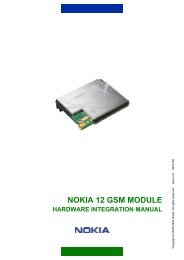
Nokia 12 GSM Module Hardware Integration ... - KORE Telematics
Nokia 12 GSM Module Hardware Integration ... - KORE Telematics
Nokia 12 GSM Module Hardware Integration ... - KORE Telematics

Create successful ePaper yourself
Turn your PDF publications into a flip-book with our unique Google optimized e-Paper software.
NOKIA <strong>12</strong> <strong>GSM</strong> MODULE<br />
HARDWARE INTEGRATION MANUAL<br />
Copyright © 2003-2004 <strong>Nokia</strong>. All rights reserved. Issue 1.3 923<strong>12</strong>30
Contents<br />
ACRONYMS AND TERMS ......................................................................................................1<br />
1. ABOUT THIS DOCUMENT ................................................................................................3<br />
2. INTRODUCTION ................................................................................................................4<br />
3. MECHANICAL INTEGRATION...........................................................................................5<br />
3.1 DIMENSIONS ...............................................................................................................5<br />
4. ELECTRICAL INTEGRATION ............................................................................................7<br />
4.1 M2M SYSTEM CONNECTOR......................................................................................7<br />
4.1.1 Electrical characteristics ........................................................................................8<br />
4.1.2 Connector pin-out ..................................................................................................9<br />
4.2 GROUNDING .............................................................................................................16<br />
4.3 POWER SUPPLY .......................................................................................................16<br />
4.4 SERIAL COMMUNICATION.......................................................................................17<br />
4.4.1 PORT1.................................................................................................................17<br />
4.4.2 PORT2.................................................................................................................18<br />
4.4.3 PORT3.................................................................................................................18<br />
4.5 SIM INTERFACE ........................................................................................................18<br />
4.6 AUDIO INTERFACE ...................................................................................................19<br />
4.6.1 Analog audio........................................................................................................19<br />
4.6.1.1 Analog audio example ..................................................................................21<br />
4.6.1.2 Acoustic echo ...............................................................................................23<br />
4.6.2 Digital audio .........................................................................................................23<br />
4.6.2.1 Sign-extended linear code ............................................................................24<br />
5. RF AND ANTENNA INTEGRATION.................................................................................26<br />
5.1 ANTENNA INSTALLATION ........................................................................................26<br />
6. TEST BOARD FOR THE NOKIA <strong>12</strong> <strong>GSM</strong> MODULE .......................................................28<br />
6.1 POWERING................................................................................................................28<br />
6.2 SIM CARD READER ..................................................................................................28<br />
6.3 RS-232 CONVERTERS..............................................................................................28<br />
6.4 AUDIO ........................................................................................................................29<br />
7. CERTIFICATIONS............................................................................................................32
7.1.1 RX-2.....................................................................................................................32<br />
7.1.2 RX-9.....................................................................................................................32<br />
7.2 TECHNICAL REQUIREMENTS .................................................................................33<br />
7.2.1 SIM testing...........................................................................................................33<br />
7.2.2 Power supply .......................................................................................................33<br />
7.2.3 EMC/ESD and safety tests ..................................................................................33<br />
7.2.4 RF testing ............................................................................................................33<br />
7.2.5 RF exposure ........................................................................................................34<br />
7.2.6 Additional type approval notes.............................................................................34<br />
REFERENCES.......................................................................................................................35<br />
APPENDIX: NOKIA <strong>12</strong> TEST BOARD PART LIST, ASSEMBLY DRAWING AND<br />
SCHEMATICS ..................................................................................................................36
Legal Notice<br />
Copyright © 2003-2004 <strong>Nokia</strong>. All rights reserved.<br />
Reproduction, transfer, distribution or storage of part or all of the contents in this document in any form without the<br />
prior written permission of <strong>Nokia</strong> is prohibited.<br />
<strong>Nokia</strong> and <strong>Nokia</strong> Connecting People are registered trademarks of <strong>Nokia</strong> Corporation. Java and all Java-based<br />
marks are trademarks or registered trademarks of Sun Microsystems, Inc. Other product and company names<br />
mentioned herein may be trademarks or trade names of their respective owners.<br />
<strong>Nokia</strong> operates a policy of continuous development. <strong>Nokia</strong> reserves the right to make changes and improvements<br />
to any of the products described in this document without prior notice.<br />
Under no circumstances shall <strong>Nokia</strong> be responsible for any loss of data or income or any special, incidental,<br />
consequential or indirect damages howsoever caused.<br />
The contents of this document are provided "as is". Except as required by applicable law, no warranties of any<br />
kind, either express or implied, including, but not limited to, the implied warranties of merchantability and fitness<br />
for a particular purpose, are made in relation to the accuracy, reliability or contents of this document. <strong>Nokia</strong><br />
reserves the right to revise this document or withdraw it at any time without prior notice.<br />
RX-9:<br />
FCC/INDUSTRY CANADA NOTICE<br />
Your device may cause TV or radio interference (for example, when using a telephone in close proximity to<br />
receiving equipment). The FCC or Industry Canada can require you to stop using your telephone if such<br />
interference cannot be eliminated. If you require assistance, contact your local service facility. This device<br />
complies with part 15 of the FCC rules. Operation is subject to the condition that this device does not cause<br />
harmful interference.
ACRONYMS AND TERMS<br />
Acronym/term<br />
A<br />
AC<br />
A/D<br />
API<br />
AT<br />
Description<br />
Ampere<br />
°C Celcius<br />
CE<br />
CORBA<br />
CMOS<br />
CSD<br />
CTS<br />
dB<br />
dBi<br />
DC<br />
DCD<br />
DCE<br />
DSR<br />
DTE<br />
DTR<br />
EARN<br />
EARP<br />
EDGE<br />
E<strong>GSM</strong><br />
EMC<br />
ESD<br />
F<br />
Alternating Current<br />
Analog-to-Digital<br />
Application Programming Interface<br />
ATtention (command language)<br />
Mark for a product that fulfils the EU safety and<br />
R&TTE requirements<br />
Common Object Request Broker Architecture<br />
Complementary Metal-Oxide Semiconductor<br />
Circuit Switched Data<br />
Clear To Send<br />
Decibel<br />
Antenna Gain<br />
Direct Current<br />
Data Carrier Detect<br />
Data Circuit Terminating Equipment<br />
Data Set Ready<br />
Data Terminal Equipment<br />
Data Terminal Ready<br />
Earphone Amplifier Inverting Input Pin<br />
Earphone Amplifier Non-Inverting Input Pin<br />
Enhanced Data Rates for Global Evolution<br />
Extended <strong>GSM</strong><br />
Electromagnetic Compatibility<br />
Electrostatic Discharge<br />
Farad<br />
°F Fahrenheit<br />
FCC<br />
GGSN<br />
GPRS<br />
Federal Communications Commission<br />
Gateway GPRS Support Node<br />
General Packet Radio Service<br />
1/44
Acronym/term<br />
GPS<br />
<strong>GSM</strong><br />
HBM<br />
Hi-Z<br />
HSCSD<br />
HW<br />
Hz<br />
IC<br />
IP<br />
M2M<br />
MICN<br />
MICP<br />
MMCX<br />
PCB<br />
PCM<br />
RF<br />
RI<br />
RS-232<br />
RTS<br />
RX-2<br />
RX-9<br />
SIM<br />
SMS<br />
SW<br />
TCP<br />
UART<br />
UDP<br />
V<br />
W<br />
Description<br />
Global Positioning System<br />
Global System for Mobile Communication<br />
Human Body Model<br />
High Impedance<br />
High Speed Circuit Switched Data<br />
<strong>Hardware</strong><br />
Hertz<br />
Integrated Circuit<br />
Internet Protocol<br />
Machine-to-machine<br />
Microphone amplifier inverting input pin<br />
Microphone amplifier non-inverting input pin<br />
Miniature Microax<br />
Printed Circuit Board<br />
Pulse Code Modulation<br />
Radio Frequency<br />
Ring Indicator<br />
Interface, standardised by the Electronic Industries<br />
Alliance (EIA), for communication between<br />
computers, terminals, and modems<br />
Request to Send<br />
Type designation for the <strong>Nokia</strong> <strong>12</strong> <strong>GSM</strong> module<br />
(E<strong>GSM</strong> 900/<strong>GSM</strong> 1800 MHz bands)<br />
Type designation for the <strong>Nokia</strong> <strong>12</strong> <strong>GSM</strong> module<br />
(<strong>GSM</strong> 850/<strong>GSM</strong> 1900 MHZ bands)<br />
Subscriber Identity <strong>Module</strong><br />
Short Message Service<br />
Software<br />
Transmission Control Protocol<br />
Universal Asynchronous Receiver/Transmitter<br />
User Datagram Protocol<br />
Volt<br />
Watt<br />
2/44
1. ABOUT THIS DOCUMENT<br />
This document provides instructions for the <strong>Nokia</strong> <strong>12</strong> <strong>GSM</strong> module (hereafter<br />
<strong>Nokia</strong> <strong>12</strong> module) hardware integration. The document is intended to help the<br />
system integrator to integrate the <strong>Nokia</strong> <strong>12</strong> module into a remote end hardware<br />
application and to gain the necessary type approvals.<br />
The document describes the mechanical, electrical and radio frequency (RF)<br />
integration as well as antenna installation. In addition the document describes<br />
the technical characteristics of the <strong>Nokia</strong> <strong>12</strong> test board, and lists the<br />
certifications and technical requirements needed for type approval.<br />
Note: For more information on the <strong>Nokia</strong> <strong>12</strong> module usage and software<br />
integration, see the <strong>Nokia</strong> <strong>12</strong> <strong>GSM</strong> <strong>Module</strong> Product Specification, <strong>Nokia</strong> M2M<br />
Platform Software Developer’s Guide and <strong>Nokia</strong> M2M Platform <strong>Nokia</strong> <strong>12</strong> <strong>GSM</strong><br />
<strong>Module</strong> IMlet Programming Guide.<br />
3/44
2. INTRODUCTION<br />
The <strong>Nokia</strong> <strong>12</strong> module has been designed for M2M (machine-to-machine)<br />
applications and other wireless solutions. There are two versions of the <strong>Nokia</strong><br />
<strong>12</strong> module:<br />
• RX-2 dual-band <strong>GSM</strong> device supporting EDGE, GPRS, HSCSD, CSD, and<br />
SMS in E<strong>GSM</strong> 900/<strong>GSM</strong> 1800 MHz bands<br />
• RX-9 dual band <strong>GSM</strong> device supporting EDGE, GPRS, CSD, SMS in <strong>GSM</strong><br />
850/<strong>GSM</strong> 1900 MHZ bands.<br />
The <strong>Nokia</strong> <strong>12</strong> module can be used in several applications due to its three<br />
different operating modes. Simple I/O applications can be easily implemented<br />
by using the <strong>Nokia</strong> <strong>12</strong> module in the User control mode that offers message<br />
personalising, secure messaging, and timing functionality for SMS controlled<br />
I/O applications. In the AT command mode, the <strong>Nokia</strong> <strong>12</strong> module can be used<br />
as a <strong>GSM</strong> modem. In modem use, all supported bearers are available. The<br />
<strong>Nokia</strong> <strong>12</strong> module is <strong>Nokia</strong> M2M Platform compatible. In the M2M system mode,<br />
the <strong>Nokia</strong> <strong>12</strong> module communicates with the server application through the<br />
<strong>Nokia</strong> M2M Gateway, and all the compatible features of the <strong>Nokia</strong> <strong>12</strong> module<br />
are available for developing a wide range of M2M applications.<br />
In addition to the different operating modes, the <strong>Nokia</strong> <strong>12</strong> module has an<br />
integrated TCP/IP stack which enables direct GPRS or <strong>GSM</strong> data connection<br />
between a remote end application and a server application. Due to the<br />
integrated TCP/IP stack, the HTTP and Socket APIs of the <strong>Nokia</strong> <strong>12</strong> are<br />
available for application development.<br />
In addition to the bearers and operating modes listed above, the <strong>Nokia</strong> <strong>12</strong><br />
supports several Java APIs, location service for external GPS module<br />
integration, reliability features like AutoPIN, <strong>GSM</strong> encryption and security<br />
codes, reset mechanism and <strong>Nokia</strong> M2M Platform authentication. Java<br />
technology support enables upgrading the application software over-the-air,<br />
and smart messaging makes the installation flexible. <strong>GSM</strong> phase 2+<br />
supplementary services enable voice application development.<br />
Note: All data bearers as well as TCP/IP are dependent on network support.<br />
4/44
3. MECHANICAL INTEGRATION<br />
The <strong>Nokia</strong> <strong>12</strong> module contains two holes for mounting screws. The screws can<br />
be used in mounting, but are not compulsory. The <strong>Nokia</strong> <strong>12</strong> module has been<br />
tested according to the automotive standard DIN 72300-3 (although not in<br />
various temperatures), and it can be integrated into various applications without<br />
the screws.<br />
3.1 DIMENSIONS<br />
The general dimensions and overall area of the <strong>Nokia</strong> <strong>12</strong> module are listed in<br />
Table 1 and Table 2.<br />
Table 1. General dimensions of the <strong>Nokia</strong> <strong>12</strong> <strong>GSM</strong> module (in millimetres<br />
and inches)<br />
Height 36 mm 1.41 inch<br />
Width 45 mm 1.77 inch<br />
Thickness 9 mm 0.35 inch<br />
Table 2. Overall area of the <strong>Nokia</strong> <strong>12</strong> <strong>GSM</strong> module (in square centimetres<br />
and square inches)<br />
Area 16.2 cm 2 2.48 inch 2<br />
The detailed physical dimensions (in millimeters) of the <strong>Nokia</strong> <strong>12</strong> module are<br />
shown in Figure 1.<br />
5/44
Figure 1. Detailed physical dimensions of the <strong>Nokia</strong> <strong>12</strong> <strong>GSM</strong> module (in<br />
millimetres)<br />
6/44
4. ELECTRICAL INTEGRATION<br />
4.1 M2M SYSTEM CONNECTOR<br />
All signals are routed through the M2M System Connector, except the antenna,<br />
which is routed through the miniature microax (MMCX) RF connector.<br />
The M2M System Connector is a 60-pin (2 rows, 30 pins per row), 1.27<br />
mm/0.05 inch pitch pin header connector. It has a frame that helps in the<br />
physical integration and also holds the <strong>Nokia</strong> <strong>12</strong> module firmly in position.<br />
The possible mating connector is described in Table 3.<br />
Table 3. Possible mating connectors for the <strong>Nokia</strong> <strong>12</strong> module<br />
Supplier Part number Description<br />
SAMTEC SFMC-130-02-S-D Female connector. Board-to-board<br />
SAMTEC SFM-130-02-S-D Female connector. Board-to-board.<br />
With alignment mark.<br />
Table 4 defines the recommended operating conditions for the actual device<br />
and/or interface operation, and Table 5 defines the absolute maximum ratings.<br />
Table 4. Recommended operating conditions<br />
Parameter Value Note<br />
Supply Voltage (V BB ) 3.6…4.0 V (3.8 V typical) Voltage must never<br />
drop below the low<br />
limit.<br />
Logic voltage (I/O<br />
voltage)<br />
DC output source or sink<br />
current (any I/O pin, user<br />
adjustable)<br />
Operating temperature<br />
range<br />
1.8…5.0 V<br />
0…5 V Upper limit<br />
depending on I/O<br />
voltage.<br />
-10…+55 °C<br />
+14…+131 °F<br />
Table 5. Absolute maximum ratings<br />
Parameter<br />
Supply voltage<br />
DC input voltage (any signal pin)<br />
Value<br />
+4.2 V<br />
-0.5…5.5 V<br />
7/44
Parameter<br />
Value<br />
Operating temperature range -25…+55 °C<br />
-13…+131 °F<br />
Storage temperature range -40…+85 °C<br />
-40…+185 °F<br />
4.1.1 Electrical characteristics<br />
All digital outputs (1-9) are open drain outputs, and all pins have a 10 kohm<br />
pull-up resistor to I/O voltage.<br />
Table 6. Digital output characteristics<br />
Parameter<br />
Application load resistance<br />
Application load capacitance<br />
High level output voltage minimum (Io=-20µA)<br />
Low level output voltage maximum (Io=1mA)<br />
Value<br />
>100 kohm<br />
Table 8. Digital input characteristics<br />
Parameter<br />
Application driving impedance<br />
Low level input voltage (IO VOLTAGE/pin 52<br />
1.8 - 5V)<br />
High level input voltage ((IO VOLTAGE/pin 52<br />
1.8 - 5V)<br />
Value<br />
Figure 2. Pin numbering of the <strong>Nokia</strong> <strong>12</strong> M2M System Connector<br />
The pin-out of the M2M System Connector in shown in Table 11.<br />
Table 11. M2M System Connector pin-out<br />
Pin Name Pin Name<br />
1 VBB 2 GND<br />
3 VBB 4 GND<br />
5 VBB 6 GND<br />
7 VBB 8 GND<br />
9 VBB 10 GND<br />
11 NC <strong>12</strong> NC<br />
13 NC 14 NC<br />
15 MICP 16 EARP<br />
17 MICN 18 EARN<br />
19 AD3 20 AD2<br />
21 PCMDCLK 22 PCMSCLK<br />
23 PCMTX 24 PCMRX<br />
25 RESET T 26 RESET A<br />
27 PORT1RX 28 NC<br />
29 PORT1TX 30 OUTPUT2<br />
31 OUTPUT3 32 OUTPUT4<br />
10/44
Pin Name Pin Name<br />
33 OUTPUT5 34 INPUT6<br />
35 INPUT5 36 AD1<br />
37 BSI 38 PORT2RX<br />
39 PORT2TX 40 PORT2RTS<br />
41 PORT2CTS 42 OUTPUT8<br />
43 INPUT8 44 OUTPUT9<br />
45 SLEEPX 46 INPUT11<br />
47 VSIM 48 SIMRST<br />
49 SIMCLK 50 SIMDATA<br />
51 SIMDET 52 IO VOLTAGE<br />
53 OUTPUT1/P3RX 54 INPUT4/P3TX<br />
55 INPUT10 56 INPUT7<br />
57 OUTPUT6 58 OUTPUT7<br />
59 INPUT9 60 NC<br />
The pin functions are described in Table <strong>12</strong>.<br />
Table <strong>12</strong>. M2M System Connector pin descriptions<br />
Pin Name Description<br />
1 VBB Device power. Voltage nominal 3.8 V, 3.6 V – 4.0 V,<br />
maximum current 2A peak. Regulated power input for<br />
the <strong>Nokia</strong> <strong>12</strong> module.<br />
All V BB pins must be connected together at the<br />
application end. The device end is not fuse-protected,<br />
so the application should provide sufficient overload<br />
protection.<br />
Current consumption can be as high as 2 A when<br />
transmitting at full power. When the <strong>Nokia</strong> <strong>12</strong> module<br />
is transmitting data, there is a current peak (max. 2A )<br />
at 4.6 ms intervals that lasts 0.577ms (1 TX slot) or<br />
1.154 ms (2 TX slots). Average power consumption is<br />
about 500 mA. The power supply should be designed<br />
according to this.<br />
If the operating voltage falls below 3.4 V, the <strong>Nokia</strong><br />
<strong>12</strong> module automatically shuts down. For more<br />
information on the power supply, see Chapter 4.3.<br />
2 GND Return ground for device power. These pins are used<br />
for device power (V BB ) return ground. Connect to<br />
common ground. All GND pins must be connected at<br />
11/44
Pin Name Description<br />
3 VBB See PIN 1<br />
4 GND See PIN 2<br />
5 VBB See PIN 1<br />
6 GND See PIN 2<br />
7 VBB See PIN 1<br />
8 GND See PIN 2<br />
9 VBB See PIN 1<br />
10 GND See PIN 2<br />
11 NC Not used<br />
<strong>12</strong> NC Not used<br />
13 NC Not used<br />
14 NC Not used<br />
the application end. For more information on<br />
grounding, see Chapter 4.2.<br />
15 MICP MICP is used with analog audio as differential<br />
positive input. The line is AC coupled at the device<br />
end. Frequency response is 300 - 3400 Hz. For more<br />
information on the analog audio, see chapter 4.6.1.<br />
16 EARP EARP is used with analog audio as differential<br />
positive output. Frequency response is 300 - 3400<br />
Hz. For more information on the analog audio, see<br />
Chapter 4.6.1.<br />
17 MICN MICN is used with analog audio as differential<br />
negative input. The line is AC coupled at the device<br />
end. Frequency response is 300 - 3400 Hz. For more<br />
information on the analog audio, see chapter 4.6.1.<br />
18 EARN EARN is used with analog audio as differential<br />
negative output. Frequency response is 300 - 3400<br />
Hz. For more information on the analog audio, see<br />
chapter 4.6.1.<br />
19 AD3 Input for 10 bit analog-to-digital (A/D) converter. The<br />
application end must scale voltage level between 0 -<br />
2.8 V.<br />
20 AD2 See PIN 19<br />
21 PCMDCLK PCMDCLK is a 5<strong>12</strong> kHz digital audio clock from the<br />
application module. Logic level is set by the IO<br />
VOLTAGE pin (pin 52). For more information on the<br />
digital audio, see Chapter 4.6.2.<br />
22 PCMSCLK PCMSCLK is one PCMDCLK cycle that repeats itself<br />
every 64 PCMDCLK cycles. Frame sync frequency is<br />
thus is 8 kHz. The logic level is set by the IO<br />
<strong>12</strong>/44
Pin Name Description<br />
VOLTAGE pin (pin 52). For more information on the<br />
digital audio, see Chapter 4.6.2.<br />
23 PCMTX Digital audio, transmits data from the device to the<br />
application. Logic level is set by the IO VOLTAGE pin<br />
(pin 52). For more information on the digital audio,<br />
see Chapter 4.6.2.<br />
24 PCMRX Digital audio, receives data from the application to the<br />
device. Logic level is set by the IO VOLTAGE pin (pin<br />
52). For more information on the digital audio, see<br />
Chapter 4.6.2.<br />
25 RESET T Reset input for the <strong>Nokia</strong> <strong>12</strong> module, active low. The<br />
<strong>Nokia</strong> <strong>12</strong> module is reset when this line is low. Logic<br />
level is set by the IO VOLTAGE pin (pin 52).<br />
Minimum duration is approximately 500 ms.<br />
26 RESET A Reset output for the application, active low. Reset<br />
goes high after approximately 170 ms of power-up.<br />
Logic level is set by the IO VOLTAGE pin (pin 52).<br />
27 PORT1RX PORT1 receive. PORT1RX is an asynchronous serial<br />
channel receive pin. Functionality otherwise as in pin<br />
29, PORT1TX. Logic level is set by the IO VOLTAGE<br />
pin (pin 52).<br />
28 NC Not used<br />
29 PORT1TX PORT1 transmit. PORT1TX is an asynchronous<br />
serial channel transmit pin that can be used with pin<br />
27 (PORT1RX) to form a full duplex serial link. Pins<br />
30-35 can be used to provide handshaking functions.<br />
Logic level is set by the IO VOLTAGE pin (pin52)<br />
30 OUTPUT2 Digital output from device. Logic level is set by the IO<br />
VOLTAGE pin (pin 52). If the AT command mode is<br />
active, this pin is used as a Data Carrier Detect<br />
(DCD) output for Port 1.<br />
31 OUTPUT3 Digital output from module. Logic level is set by the<br />
IO VOLTAGE pin (pin 52). If the AT command mode<br />
is active, this pin is used as Data Set Ready (DSR)<br />
output for Port 1.<br />
32 OUTPUT4 Digital output from module. Logic level is set by the<br />
I/O voltage pin (pin 52). If the AT command mode is<br />
active, this pin is used as Clear To Send (CTS) output<br />
for Port 1.<br />
33 OUTPUT5 Digital output from module. Logic level is set by the<br />
IO VOLTAGE pin (pin 52). If the AT command mode<br />
is active, this pin is used as Ring Indicator (RI) output<br />
for Port 1.<br />
34 INPUT6 Digital input to module. Logic level is set by the IO<br />
VOLTAGE pin (pin 52). If the AT command mode is<br />
active, this pin is used as Request To Send (RTS)<br />
13/44
Pin Name Description<br />
input for Port 1.<br />
35 INPUT5 Digital input to module. Logic level is set by the IO<br />
VOLTAGE pin (pin 52). If the AT command mode is<br />
active, this pin is used as Data Terminal Ready (DTR)<br />
input for Port 1<br />
36 AD1 Input for 10 bit A/D converter. The application end<br />
must scale voltage level between 0 to 2.8 V.<br />
37 BSI Input for 10 bit A/D converter. The application end<br />
must scale voltage level between 0 to 2.8 V.<br />
38 PORT2RX PORT2 receive. PORT2RX is an asynchronous serial<br />
channel receive pin and it is used with pin 39. Logic<br />
level is set by the IO VOLTAGE pin (pin 52).<br />
39 PORT2TX PORT2 Transmit. PORT2RX is an asynchronous<br />
serial channel transmit pin that is used with pin 38.<br />
Logic level is set by the IO VOLTAGE pin (pin 52).<br />
40 PORT2RTS RTS for PORT2. PORT2RTS provides handshaking<br />
signal for asynchronous communication between the<br />
<strong>Nokia</strong> <strong>12</strong> module and the application when using<br />
PORT2. Works together with pin 41. Logic level is set<br />
by the IO VOLTAGE pin (pin 52).<br />
41 PORT2CTS CTS for PORT2. PORT2CTS provides handshaking<br />
signal for asynchronous communication between the<br />
<strong>Nokia</strong> <strong>12</strong> module and the application when using<br />
PORT2. Works together with pin 40. Logic level is set<br />
by the IO VOLTAGE pin (pin 52).<br />
42 OUTPUT8 Digital output from the <strong>Nokia</strong> <strong>12</strong> module. Logic level is<br />
set by the IO VOLTAGE pin (pin 52).<br />
43 INPUT8 Digital input to the <strong>Nokia</strong> <strong>12</strong> module. Logic level is set<br />
by the IO VOLTAGE pin (pin 52).<br />
44 OUTPUT9 Digital output from the <strong>Nokia</strong> <strong>12</strong> module. Logic level is<br />
set by the IO VOLTAGE pin (pin 52).<br />
45 SLEEPX Sleep indicator of the <strong>Nokia</strong> <strong>12</strong> module. When the<br />
<strong>Nokia</strong> <strong>12</strong> module is in the sleep mode, the level of<br />
this output pin is low, otherwise high. The sleep mode<br />
is automatic. Logic level is set by the IO VOLTAGE<br />
pin (pin 52).<br />
46 INPUT11 Digital input to the <strong>Nokia</strong> <strong>12</strong> module. Logic level is set<br />
by the IO VOLTAGE pin (pin 52).<br />
47 VSIM Operating voltage for the SIM card, generated by the<br />
<strong>Nokia</strong> <strong>12</strong> module. For more information on the SIM<br />
interface, see Chapter 4.5.<br />
48 SIMRST Reset signal for the SIM card, generated by the <strong>Nokia</strong><br />
<strong>12</strong> module. For more information on the SIM<br />
interface, see Chapter 4.5.<br />
14/44
Pin Name Description<br />
49 SIMCLK Clock signal for the SIM card, generated by the <strong>Nokia</strong><br />
<strong>12</strong> module. For more information on the SIM<br />
interface, see Chapter 4.5.<br />
50 SIMDATA Data line between the SIM card and the <strong>Nokia</strong> <strong>12</strong><br />
module. For more information on the SIM interface,<br />
see Chapter 4.5.<br />
51 SIMDET SIM card detection signal. For more information on<br />
the SIM interface, see Chapter 4.5.<br />
52 IO VOLTAGE This pin sets logic level for the application. Voltage<br />
must be 1.8 V - 5.0 V. For more information on the<br />
power supply, see Chapter 4.3.<br />
53 OUTPUT1 /<br />
PORT3RX<br />
Digital output from the <strong>Nokia</strong> <strong>12</strong> module. Logic level is<br />
set by the IO VOLTAGE pin (pin 52). If PORT3 is<br />
configured for serial communication, this is a receive<br />
(input) signal.<br />
54 INPUT4 /<br />
PORT3TX<br />
Note! Direction changes if pin 53 is configured for<br />
serial communication.<br />
Digital input to the <strong>Nokia</strong> <strong>12</strong> module. Logic level is set<br />
by the IO VOLTAGE pin (pin 52). If PORT3 is<br />
configured for serial communication, this is a<br />
transmitter (output) signal.<br />
Note! Direction changes if pin 54 is configured for<br />
serial communication.<br />
55 INPUT10 Digital input to the <strong>Nokia</strong> <strong>12</strong> module. Logic level is set<br />
by the IO VOLTAGE pin (pin 52).<br />
56 INPUT7 Digital input to the <strong>Nokia</strong> <strong>12</strong> module. Logic level is set<br />
by the IO VOLTAGE pin (pin 52).<br />
57 OUTPUT6 Digital output from the <strong>Nokia</strong> <strong>12</strong> module. Logic level is<br />
set by the IO VOLTAGE pin (pin 52).<br />
58 OUTPUT7 Digital output from the <strong>Nokia</strong> <strong>12</strong> module. Logic level is<br />
set by the IO VOLTAGE pin (pin 52).<br />
59 INPUT9 Digital input to the <strong>Nokia</strong> <strong>12</strong> module. Logic level is set<br />
by the IO VOLTAGE pin (pin 52).<br />
60 NC Not used<br />
15/44
4.2 GROUNDING<br />
There is only one common ground for the power supply and I/Os in the <strong>Nokia</strong><br />
<strong>12</strong> module. That is, there are no separate analog/digital ground pins in the M2M<br />
System Connector.<br />
All ground pins must be connected together at the application end. Grounding<br />
through screws is not allowed. The mounting screws must be isolated from the<br />
application ground.<br />
4.3 POWER SUPPLY<br />
The <strong>Nokia</strong> <strong>12</strong> module is powered by the hardware application to which it is<br />
integrated. The operating voltage must not fall below the specification limit<br />
under any circumstances. The recommended operation conditions are shown in<br />
Table 4. For example, at full power, the TX can be up to 2 A, when current is<br />
drawn from the power supply. There are no capacitors on the power supply line<br />
of the <strong>Nokia</strong> <strong>12</strong> module, so the application must provide sufficient filtering.<br />
The power supply must be capable of supplying at least 3 W average power,<br />
but it is recommended that the power supply also provides the peak current.<br />
Otherwise a large capacitor bank is needed to compensate the voltage drop<br />
during transmit bursts.<br />
The <strong>Nokia</strong> <strong>12</strong> module does not have protection for over-voltage of current, so<br />
the hardware application must be equipped with one if there is a possibility for<br />
over-voltage. The hardware application should at least include a fuse.<br />
The ripple on the operating voltage must not exceed 100 mV and the voltage<br />
must never drop below 3.6 V during operation.<br />
The application must also produce I/O voltage. The logic levels of digital inputs<br />
and outputs correspond to this I/O voltage. I/O voltage can be supplied from a<br />
linear regulator.<br />
16/44
Figure 3. Example powering with simple DC/DC converter and linear<br />
regulator<br />
4.4 SERIAL COMMUNICATION<br />
The <strong>Nokia</strong> <strong>12</strong> module is accessible through three different asynchronous serial<br />
interfaces with different protocols. The pins provide one asynchronous channel<br />
with a simple handshaking capability. The usage of the 3 ports can be<br />
configured with the <strong>Nokia</strong> <strong>12</strong> Configurator software. The <strong>Nokia</strong> <strong>12</strong> Configurator<br />
is downloadable at www.forum.nokia.com/m2m free of charge.<br />
The <strong>Nokia</strong> <strong>12</strong> module supports the industry standard DB9 RS-232C connection,<br />
but an external level converter is required. For more information on the<br />
available handshake signals for different ports, see Chapters 4.4.1, 4.4.2 and<br />
4.4.3.<br />
The <strong>Nokia</strong> <strong>12</strong> module is a DCE (Data Communication Equipment) and the<br />
hardware application to which it is integrated is a DTE (Data Terminal<br />
Equipment). One possible method of implementing the level conversions is to<br />
use a MAX3237 transceiver or an equivalent integrated circuit (IC) level<br />
converter.<br />
Note: When port settings are changed, the new settings will not become valid<br />
until the <strong>Nokia</strong> <strong>12</strong> module is restarted.<br />
4.4.1 PORT1<br />
PORT1 provides the first asynchronous channel. This port can be used with full<br />
8 signal RS-232 handshaking signals. The baud rate for PORT1 can be<br />
between <strong>12</strong>00 and 230400 bit/s.<br />
17/44
Note: Baud rate 230400 bit/s can be used only with AT command mode and<br />
autobauding.<br />
There are several settings for PORT1. The default setting for PORT1 is ‘HW<br />
Detection’. This means that when a 68 kohm resistor is set between the BSI<br />
(pin 37) and the ground, the <strong>Nokia</strong> <strong>12</strong> module enters the AT command mode<br />
when it is started. It is also possible to set the AT command mode on by using<br />
the <strong>Nokia</strong> <strong>12</strong> Configurator (the connection type is set to ‘AT’).<br />
The <strong>Nokia</strong> <strong>12</strong> module provides all signals for the industry standard DB9 RS-<br />
232C connection, but an external level converter is required.<br />
4.4.2 PORT2<br />
PORT2 provides the second asynchronous channel with a simple handshaking<br />
capability (only RTS and CTS). The baud rate for PORT2 can be set to 9600,<br />
19200, 38400, 57600 or 115200 bit/s. PORT2 is the default port for using the<br />
M2M System Protocol. However, if PORT1 is configured to use the M2M<br />
System Protocol, PORT2 cannot be used.<br />
4.4.3 PORT3<br />
PORT3 provides the third asynchronous channel with no hardware<br />
handshakes. The baud rate for PORT3 can be set between <strong>12</strong>00 and 115200<br />
bit/s.<br />
4.5 SIM INTERFACE<br />
All leads from the M2M System Connector to the SIM card reader must be<br />
shorter than 15 cm/5.9 inches, because the voltage drop and increasing<br />
capacitance will affect timing. Furthermore, it is recommended that a 100 nF<br />
bypass capacitor is placed as close as possible to the SIM reader on the VSIM<br />
(pin47) line.<br />
The leads between the M2M System Connector and the SIM card reader must<br />
be protected against interferences, and that is why the striplines must always<br />
be placed within the interlayers of the printed circuit board (PCB).<br />
Note: The striplines must never be placed to the overlayer of the PCB.<br />
A possible SIM card reader supplier is listed in Table 13.<br />
Table 13. Possible SIM card reader supplier<br />
18/44
Supplier Part Number Description<br />
Amphenol M-C707_10M006_522_2 SIM reader with a lid open<br />
indication switch.<br />
DATA NC GND<br />
7 5 5<br />
3 2 1<br />
CLK RST VSIM<br />
Figure 4. SIM card connections (using Amphenol)<br />
The <strong>Nokia</strong> <strong>12</strong> module supports 1.8 V and 3 V SIM cards, and it automatically<br />
sets the correct voltage according to the SIM card that is used.<br />
Note: The SIM card reader must have a switch that indicates when the SIM card<br />
is being removed, so that the <strong>Nokia</strong> <strong>12</strong> module can shut it down correctly. The<br />
switch must open when the card is removed or the lid is open. The <strong>Nokia</strong> <strong>12</strong><br />
module has a pull-up in the SIM detection line, so the hardware application must<br />
connect the other end of the switch to the ground.<br />
4.6 AUDIO INTERFACE<br />
4.6.1 Analog audio<br />
The M2M System Connector provides possibilities to build different kind of<br />
audio applications around the <strong>Nokia</strong> <strong>12</strong> module.<br />
19/44
The analog TX path (from the external application to the <strong>Nokia</strong> <strong>12</strong> module) has<br />
a DC isolation inside the <strong>Nokia</strong> <strong>12</strong> module with 100 nF capacitors, and these<br />
capacitors together with the microphone preamplifier input impedance form a 1 st<br />
order high pass filter with 32 Hz roll-off (-3 dB).<br />
Table 14. Microphone audio characteristics<br />
Name Symbol Min Type Max Units<br />
Differential input<br />
voltage range for<br />
microphone input<br />
(MICP & MICN)<br />
Microphone amplifier<br />
input resistor<br />
Common mode voltage<br />
level<br />
0.316 2.0 V PP<br />
RMIC 30 50 kohm<br />
VCM 1.3 1.35 1.4 V<br />
The earphone lines from the <strong>Nokia</strong> <strong>12</strong> module are driven differentially to<br />
achieve the best possible audio quality, free of radio frequency noise. In the<br />
differential mode, positive output is driven from EARP and negative signal from<br />
EARN output.<br />
Table 15. Earphone audio characteristics<br />
Name Test condition Min Type Max Units<br />
Output voltage swing<br />
in fully differential<br />
mode<br />
EARP to EARN 0.316 2 V PP<br />
Output resistance 1 ohm<br />
Load resistance<br />
Load resistance<br />
Load capacitance<br />
Common voltage level<br />
for Earphone output<br />
EARP to EARN<br />
(with dynamic<br />
transducer)<br />
EARP to EARN<br />
(with external<br />
audio circuitry)<br />
EARP to EARN<br />
(with external<br />
audio circuitry)<br />
30 45 ohm<br />
1 kohm<br />
10 nF<br />
VCMEar 0.75 0.8 0.85 V<br />
Offset voltage -50 50 mV<br />
20/44
The following chapter gives an example of using the audio properties of the<br />
<strong>Nokia</strong> <strong>12</strong> module for voice communication purposes. The circuits presented in<br />
the example illustrate the connection methods.<br />
There are also other possibilities for using the <strong>Nokia</strong> <strong>12</strong> audio interface. The<br />
presented component values are examples only; the customer can adjust the<br />
application-specific values to achieve the best performance for the application<br />
in question.<br />
4.6.1.1 Analog audio example<br />
Analog TX path: Due to the small audio signal level of the electret microphone,<br />
it is recommended to use a preamplifier for the microphone before connecting it<br />
to the <strong>Nokia</strong> <strong>12</strong> module. It is strongly recommended to protect the differential<br />
connection against RF noise. A microphone preamplifier with 20 dB input gain<br />
is recommended for reasonable uplink audio levels.<br />
Microphone input: See Figure 5.<br />
VANA<br />
R5<br />
R4<br />
VANA<br />
C1<br />
VANA<br />
R3<br />
-<br />
C2<br />
MicP<br />
R1<br />
+<br />
R6<br />
R7<br />
VANA<br />
R2<br />
-<br />
+<br />
C3<br />
MicN<br />
Figure 5. Single-ended microphone pre-amplifier<br />
Analog RX path: In voice applications, the <strong>Nokia</strong> <strong>12</strong> module is able to drive an<br />
earphone application without external electronics. However, it is also possible<br />
to build a high-volume loudspeaker application by using an external power<br />
amplifier with a high sensitivity loudspeaker. The following paragraphs show<br />
example circuits for both cases.<br />
21/44
Earphone application: An earphone can be connected to the <strong>Nokia</strong> <strong>12</strong> module<br />
without external components. In Figure 6 external components are used for<br />
EMC purposes to optimise audio quality and reliability.<br />
R1<br />
L1<br />
R2<br />
C1<br />
C2<br />
J1<br />
J2<br />
Figure 6. Earphone application circuit<br />
The recommended earphone type is dynamic. The maximum allowed load for<br />
this application is 32 ohm. In the example circuit, L1 is the common mode<br />
choke for the suppression of common mode disturbance in the earphone lines.<br />
J1 and J2 are surge protector gaps for ESD protection. These can be replaced<br />
with varistor or any other state-of-the-art ESD protection component. C1 and<br />
C2 are used for RF noise filtering.<br />
R1 and R2 are used as an attenuator if the signal level from the <strong>Nokia</strong> <strong>12</strong><br />
module is too high for the application. These resistors can be replaced with<br />
linear potentiometers and thus get adjustable volume control for the earphone<br />
application. The following component list gives example values for the circuit:<br />
• L1= 1000ohm@100MHz<br />
• C1=C2=27pF<br />
• R1=R2= Must be defined together with the sensitivity of the earphone<br />
External Audio Power amplifier: External audio power must be used if there<br />
is a need to drive low impedance load as loudspeaker. Figure 7 shows an<br />
example connection circuit for differential audio boomer. In this application only<br />
the connection interface to the <strong>Nokia</strong> <strong>12</strong> module is presented. For more detailed<br />
information on the boomer connections and specification, see the boomer<br />
manufacturer application note.<br />
22/44
VDD<br />
C4<br />
R2<br />
Differential Audio<br />
Boomer<br />
VDD<br />
EarP<br />
EarN<br />
C1<br />
C2<br />
R1<br />
R3<br />
-<br />
+<br />
R5<br />
R4<br />
VDD<br />
R6<br />
Bypass<br />
-<br />
C3<br />
Bias<br />
+<br />
Shutdown control<br />
Figure 7. Differential external power amplifier connection<br />
Refer to the audio boomer manufacturer and loudspeaker application notes for<br />
information on maximum safe ratings for the selected components. Also keep in<br />
mind the limitation of V DD to avoid overdriving the audio boomer and thus<br />
distorting the output signal unnecessarily.<br />
4.6.1.2 Acoustic echo<br />
Because in a <strong>GSM</strong> voice call the uplink and downlink audios are activated at<br />
the same time, it is recommended to use common sense when evaluating a<br />
suitable distance between the loudspeaker and the microphone. The acoustic<br />
echo canceller inside the <strong>Nokia</strong> <strong>12</strong> module is tuned so that the optimum result<br />
is achieved with 20 cm or longer distance between the microphone and the<br />
speaker. It is also advisable to locate the microphone and the loudspeaker so<br />
that they are pointed away from each other to achieve the best possible doubletalk<br />
performance.<br />
4.6.2 Digital audio<br />
There is a pulse code modulation (PCM) codec interface in the <strong>Nokia</strong> <strong>12</strong><br />
module for digital audio support. The digital audio interface supports signextended<br />
13-bit linear code (total 16 bits are transmitted).<br />
23/44
4.6.2.1 Sign-extended linear code<br />
PCM digital audio data transmission between the <strong>Nokia</strong> <strong>12</strong> module and the<br />
application is handled with four signals: PCMDCLK, PCMSCLK, PCMTX, and<br />
PCMRX. The format of the data transmission is sign-extended 13-bit linear<br />
code. A total of 16 bits are transmitted, and higher order bits must be signextended.<br />
Transmission of data commences after frame sync (PCMSCLK) rises<br />
high for one PCMDCLK clock cycle. After returning low, each data bit is<br />
transmitted on the falling edge of PCMDCLK.<br />
PCMDClk<br />
PCMSClk<br />
PCMTxData<br />
PCMRxData<br />
15 14 13 <strong>12</strong> 11 10<br />
MSB<br />
Sign extended<br />
15 14 13 <strong>12</strong> 11 10<br />
MSB<br />
Sign extended<br />
0<br />
LSB<br />
0<br />
LSB<br />
Figure 8. Timing of clock and transmission signals<br />
The application must provide both the PCMDCLK and PCMSCLK. PCMDCLK<br />
frequency is 5<strong>12</strong> kHz and PCMSCLK is repeated at 8 kHz, that is, at every 64th<br />
clock cycle. All bits but the 16 data bits following the frame sync are discarded.<br />
PCMDCLK has a typical 50 % duty-cycle; a variation of 5 % can be tolerated.<br />
For detailed timing, refer to Figure 9 and Table 16. Tcyc is the cycle time (1.953<br />
microseconds) of the 5<strong>12</strong> kHz clock. The PCMSCLK rising edge must occur at<br />
the maximum of 8 ns after the PCMSCLK rising edge.<br />
The pulse width of the frame sync pulse should be one data clock cycle.<br />
PCMDClk<br />
Td(SCL)<br />
PCMSClk<br />
Td(PCMTxData)<br />
PCMTxData<br />
PCMRxData<br />
Th(PCMRxData)<br />
Tsu(PCMRxData)<br />
MSB<br />
MSB<br />
Figure 9. PCM timing diagram<br />
24/44
PCM timing characteristics are described in Table 16. The coding format<br />
presented in Table 16 is supported, for example, by the Motorola type<br />
MC145483 codec.<br />
Table 16. PCM timing characteristics<br />
Parameter Symbol Min Max Unit<br />
Delay time (PCMSClk valid after<br />
PCMDClk rising)<br />
Delay time (PCMTxData valid<br />
after PCMDClk rising)<br />
PCMRxData setup time before<br />
PCMDClk falling edge<br />
PCMRxData hold time after<br />
PCMDClk falling edge<br />
Td(SClk) 0 8 ns<br />
Td(TxData) 5 25 ns<br />
Tsu(RxData) 20 Tcyc-20 ns<br />
Th(RxData) 20 Tcyc-20 ns<br />
25/44
5. RF AND ANTENNA INTEGRATION<br />
The RF requirements for the <strong>Nokia</strong> <strong>12</strong> module are type-dependent:<br />
• RF requirements for the RX-2 type follow the ETSI E<strong>GSM</strong>900/<strong>GSM</strong>1800<br />
phase2+ specifications.<br />
• RF requirements for the RX-9 type follow the ETSI <strong>GSM</strong>850/<strong>GSM</strong>1900<br />
phase2+ specifications.<br />
Table 17. RF specifications for the <strong>Nokia</strong> <strong>12</strong> <strong>GSM</strong> module<br />
Parameter Value Description<br />
RF impedance 50 ohm<br />
RF power 2W (class 4) E<strong>GSM</strong>900 & <strong>GSM</strong> 850<br />
1W (class 1) <strong>GSM</strong>1800 & <strong>GSM</strong> 1900<br />
The RF signal from the <strong>Nokia</strong> <strong>12</strong> module to an external antenna goes trough<br />
the MMCX connector.<br />
An adapter cable between the MMCX connector and the antenna may be<br />
needed. Suitable connectors and cables are available, for example, from<br />
Amphenol, TYCO, and IMS Connector Systems.<br />
The <strong>Nokia</strong> <strong>12</strong> module is certified with a Smarteq dual-band antenna (art no:<br />
1140.26 for 900/1800MHz and 1140.27 for 850/1900MHz). Suitable antennas<br />
are available, for example, from Smarteq and Hirschmann.<br />
For more information on the RF exposure, see Chapter 7.2.5.<br />
5.1 ANTENNA INSTALLATION<br />
The antenna must be placed within a good RF field; a location where the signal<br />
strength is adequate. A hand-portable phone can be used to check the best<br />
location for the antenna.<br />
Note: Electronic devices can cause interference, which affects the performance of<br />
the <strong>Nokia</strong> <strong>12</strong> module. Do not place the antenna close to electronic devices or<br />
other antennas.<br />
If an additional cable is needed between the antenna and the <strong>Nokia</strong> <strong>12</strong> module,<br />
use low-loss cables (for example RG-58. Amphenol, Suhner, etc.) and<br />
connectors. Every additional cable, adapter, and connector increases the loss<br />
of signal power.<br />
26/44
When designing the hardware application to which the <strong>Nokia</strong> <strong>12</strong> module is<br />
integrated into, it is important to take care of RF emissions. Do not place any<br />
sensitive components or striplines near the antenna or the antenna connector.<br />
For more information on the RF exposure, see Chapter 7.2.5.<br />
27/44
6. TEST BOARD FOR THE NOKIA <strong>12</strong> <strong>GSM</strong> MODULE<br />
The <strong>Nokia</strong> <strong>12</strong> test board is a hardware development tool for application<br />
developers and system integrators. It manages DC voltages, SIM card, I/O’s,<br />
and audios. You can measure several interfaces by pin headers, and the<br />
software interfaces of the D9 connectors can be seen and handled. The device<br />
can be reset with the reset button on the test board PCB.<br />
The <strong>Nokia</strong> <strong>12</strong> module has been type approved with the <strong>Nokia</strong> <strong>12</strong> test board. For<br />
more information on the <strong>Nokia</strong> <strong>12</strong> test board, see Appendix: <strong>Nokia</strong> <strong>12</strong> test<br />
board part list, assembly drawing and schematics.<br />
6.1 POWERING<br />
A 3A step down converter is used to produce module V CC . Low ESR capacitors<br />
are used.<br />
Table 18. Powering for the <strong>Nokia</strong> <strong>12</strong> test board<br />
6.2 SIM CARD READER<br />
The SIM card reader is directly connected to the M2M System Connector. The<br />
VSIM (pin47) decoupling capacitor must be present in all designs. To see the<br />
connections between the SIM card reader and the M2M System Connector, see<br />
Figure 4.<br />
6.3 RS-232 CONVERTERS<br />
All three serial ports of the <strong>Nokia</strong> <strong>12</strong> module are equipped with RS-232 level<br />
translators and D9 connector in the test board. If they are not used, there is a<br />
switch that can be used to set the converters in the Hi-Z mode.<br />
28/44
6.4 AUDIO<br />
For testing analog audio, the test board includes a connector for the <strong>Nokia</strong><br />
HSU-3 handset. The HSU-3 handset can be purchased from <strong>Nokia</strong> dealers.<br />
Figure 10. <strong>Nokia</strong> <strong>12</strong> test board microphone amplifier<br />
The <strong>Nokia</strong> <strong>12</strong> test board and its key components are shown in Figure 11.<br />
Figure 11. <strong>Nokia</strong> <strong>12</strong> test board components<br />
The <strong>Nokia</strong> <strong>12</strong> test board includes the following switches:<br />
29/44
• RS-232 translator switches for PORT1 and PORT2/PORT3<br />
−<br />
−<br />
When the RS-232 translators are on, PORT1 and PORT2/PORT3 are<br />
connected the <strong>Nokia</strong> <strong>12</strong> module via the M2M System Connector.<br />
When the RS-232 translators are off, PORT1 and PORT2/PORT3 are<br />
not connected the <strong>Nokia</strong> <strong>12</strong> module via the M2M System Connector.<br />
When the RS-232 translators are off, it is possible to establish a<br />
connection to the <strong>Nokia</strong> <strong>12</strong> module by using the pin headers (1-4).<br />
• Microphone input selection switches<br />
−<br />
−<br />
MIC FROM HSU-3 means that microphone signals are routed from the<br />
HSU- 3 connector on the testboard to the <strong>Nokia</strong> <strong>12</strong> module.<br />
MIC FROM PIN HEADER means that microphone signals are routed to<br />
pins 10 and 11 in pin header X100 on testboard edge.<br />
• Communication mode switches<br />
−<br />
−<br />
When the switches are in the normal mode position, the BSI line of the<br />
<strong>Nokia</strong> <strong>12</strong> module is floating.<br />
When the switches are in the AT mode position, a 68 kohm resistor is<br />
connected between the <strong>Nokia</strong> <strong>12</strong> module BSI line and ground.<br />
Note: To use the normal mode/AT mode settings on the test board, the<br />
connection type setting on the <strong>Nokia</strong> <strong>12</strong> Configurator must be set to ‘HW<br />
Detection’. If the connection type setting on the <strong>Nokia</strong> <strong>12</strong> Configurator is set to<br />
‘AT’, the communication mode switch settings on the <strong>Nokia</strong> <strong>12</strong> test board are<br />
overridden.<br />
The use of the switches on the <strong>Nokia</strong> <strong>12</strong> test board is illustrated in Figure <strong>12</strong>.<br />
30/44
Figure <strong>12</strong>. <strong>Nokia</strong> <strong>12</strong> test board switch usage<br />
31/44
7. CERTIFICATIONS<br />
The test house requires the following documentation from the application<br />
integrator for type approval tests:<br />
• <strong>Hardware</strong> description<br />
• Schematics<br />
• Block diagram<br />
• PWB/component layout<br />
• Bill of materials<br />
• HW/SW versions used in tests.<br />
• Summary of application<br />
• User’s guide<br />
If the application HW or SW changes, the integrator is responsible for verifying<br />
the effect, and if needed, to perform all required tests again in an accredited<br />
laboratory.<br />
7.1.1 RX-2<br />
The <strong>Nokia</strong> <strong>12</strong> module (RX-2) is a CE marked device. In order to show<br />
compliance to R&TTE requirements, the integrator has to show that all the<br />
instructions in this document have been followed in the integration, and a<br />
declaration of conformity has been written.<br />
The final product must carry CE marking to show compliance with all the<br />
directives that are applicable to it. The numbers of all the Notified Bodies<br />
involved in every aspect of the conformity assessment must be shown next to<br />
the CE marking with any additional markings that can be needed (for example,<br />
Alert symbol for WLAN). The technical documentation explains the role of each<br />
Notified Body. If external elements are designed according to this document,<br />
only the following tests must be carried out in an accredited laboratory:<br />
• EMC tests in all working modes (EN 301 489-1/7, 3GPP TS 51.010)<br />
• Safety (Europe: EN/IEC 60950)<br />
7.1.2 RX-9<br />
The <strong>Nokia</strong> <strong>12</strong> module (RX-9) is an FCC equipment authorized device (47CFR<br />
15, 22, 24). If external elements are designed according to this document, only<br />
the following tests must be carried out in an accredited laboratory:<br />
32/44
• FCC equipment authorization (all applicable parts of 47CFR15)<br />
7.2 TECHNICAL REQUIREMENTS<br />
7.2.1 SIM testing<br />
SIM testing is not needed, because the SIM card reader is a passive<br />
component. In the implementation, SIM presence must follow the type approval<br />
conditions of the <strong>Nokia</strong> <strong>12</strong> module. 6- or 8-pin SIM card readers can be used.<br />
For more information on the SIM interface, see Chapter 4.5.<br />
7.2.2 Power supply<br />
The power supply must be designed as advised in Chapter 4.3. If this<br />
specification is exactly followed and fulfilled, the number of required RF tests is<br />
minimized in the type approval process.<br />
Note: If the power supply specification is not followed, the <strong>Nokia</strong> <strong>12</strong> module type<br />
approval is not valid.<br />
7.2.3 EMC/ESD and safety tests<br />
EMC and safety tests according to <strong>GSM</strong> standards (EN 301 489-1/7, 3GPP TS<br />
51.010 and EN 60 950) are mandatory and must be completed by the<br />
application integrator. The integrator should guarantee overall ESD protection<br />
in the integrated application (EN 301 489).<br />
Note: The <strong>Nokia</strong> <strong>12</strong> test board is an ESD supersensitive device.<br />
7.2.4 RF testing<br />
The antenna must be connected to the <strong>Nokia</strong> <strong>12</strong> module as this document<br />
instructs. The antenna impedance has to be as specified in Chapter 5. Further<br />
passive RF testing for the type approval is not required. Radiation performance<br />
is always the responsibility of the integrator.<br />
Note: If the antenna specification is not followed, the <strong>Nokia</strong> <strong>12</strong> type approval is not<br />
valid.<br />
33/44
7.2.5 RF exposure<br />
In order to comply with the RF exposure requirements, install the antenna so<br />
that a minimum separation distance of 20 cm/7.9 inch can be maintained<br />
between the antenna and all persons.<br />
If some other antenna than the one in the sales package is used, it must be<br />
ensured that the maximum antenna gain of 3 dBi is not exceeded.<br />
RX-2<br />
If the application does not provide a separation distance of at least 20 cm/7.9<br />
inch, the integrator must carry out all needed certifications.<br />
RX-9<br />
The <strong>Nokia</strong> <strong>12</strong> module cannot be used in applications that allow the separation<br />
distance between antenna and all persons to be less than 20 cm/7.9 inch.<br />
7.2.6 Additional type approval notes<br />
Changes in the application software have no effect on type approval issues.<br />
If the <strong>Nokia</strong> <strong>12</strong> module software is updated, no type approval actions are<br />
required from the application integrator. All <strong>Nokia</strong> products are officially type<br />
approved.<br />
Any changes to the RF path are not allowed. Power supply instructions must be<br />
followed.<br />
RX-9<br />
The <strong>Nokia</strong> <strong>12</strong> module (RX-9) type label has the FCC ID number to indicate that<br />
it is FCC equipment authorized. If the application prevents the label from being<br />
visible, the application must be labeled so that it contains the text: “Contains<br />
FCC ID LJPRX-9”.<br />
34/44
REFERENCES<br />
<strong>Nokia</strong> M2M customer documents<br />
The following <strong>Nokia</strong> M2M customer documents are available at<br />
http://www.forum.nokia.com/m2m or http://www.americas.forum.nokia.com.<br />
/1/ <strong>Nokia</strong> M2M Platform Software Developer’s Guide<br />
/2/ <strong>Nokia</strong> M2M Platform <strong>Nokia</strong> <strong>12</strong> <strong>GSM</strong> <strong>Module</strong> IMlet Programming Guide<br />
/3/ <strong>Nokia</strong> <strong>12</strong> <strong>GSM</strong> <strong>Module</strong> Product Specification<br />
General standards and specifications<br />
/1/ 3GPP TS 51.010, Digital cellular telecommunication system (Phase 2+)<br />
Mobile Station (MS) conformance specification<br />
/ 3rd Generation Partnership Project (3GPP)<br />
/2/ 47CFR 15, 22, 24,Code of Federal Regulations, 47: Telecommunication<br />
Part 15: Radio frequency devides<br />
Part 22: Public mobile services<br />
Part 24: Personal communications services<br />
/ Federal Communications Commission (FCC)<br />
/3/ DIN 72300-3 Electrical and electronic equipment for road vehicles -<br />
Environmental condititons - Part 3: Mechanical loads<br />
/ Deutsches Institut fur Normung (DIN)<br />
/4/ EN 301 489-1/7 Electromagnetic compatibity and Radio spectrum Matters<br />
(ERM); Electro-Magnetic Compatibility (EMC) standard for radio<br />
equiment and services<br />
Part 1: Common tecnical requirements<br />
Part 7: Specific conditions for mobile and portable radio and ancillary<br />
equipment of digital cellular radio telecommunications systems (<strong>GSM</strong> and DCS)<br />
/ European Telecommunications Standards Institute (ETSI)<br />
/5/ EN/IEC 60950 Safety of Information technology equipment<br />
/ European Committee for Electrotecnical Standardization (Cenelec)<br />
35/44
APPENDIX: NOKIA <strong>12</strong> TEST BOARD PART LIST, ASSEMBLY<br />
DRAWING AND SCHEMATICS<br />
This appendix includes the <strong>Nokia</strong> <strong>12</strong> test board part list, assembly drawing and<br />
schematics. The reference numbers and x/y axis indicators on the part list can<br />
be used to locate the <strong>Nokia</strong> <strong>12</strong> test board parts on the assembly drawing.<br />
Table 19. <strong>Nokia</strong> <strong>12</strong> test board part list<br />
Ref. X Y Component<br />
Component<br />
value<br />
C100 J 13 Chipcap X7R 10% 50V 0402 1n0 50V<br />
C101 J 14 Cer. cap 10uF 16V Z <strong>12</strong>10 10u 16V<br />
C102 I 14 Tantal cap 20% 35V 100n_35V 35V<br />
C103 I 14 Tantal cap 20% 35V 100n_35V 35V<br />
C104 K 13 CHIPCAP X5R 100N K 10V 0402 100n 10V<br />
C105 K 13 Chipcap 5% NP0 22p 50V<br />
C106 K 13 Chipcap 5% NP0 22p 50V<br />
C107 K 13 CHIPCAP X5R 100N K 10V 0402 100n 10V<br />
C108 K 13 Chipcap 5% NP0 22p 50V<br />
C109 K 14 CHIPCAP NP0 180P J 25V 0402 180p 25V<br />
C110 K 14 Chipcap 5% NP0 22p 50V<br />
C111 K 13 CHIPCAP NP0 180P J 25V 0402 180p 25V<br />
C1<strong>12</strong> K <strong>12</strong> Chipcap 5% NP0 22p 50V<br />
C113 M 14 CHIPCAP X5R 1U0 10V 0805 1u0 10V<br />
C114 M 13 CHIPCAP X5R 1U0 10V 0805 1u0 10V<br />
C115 M 13 Chipcap 5% NP0 150p 50V<br />
C116 M 13 CHIPCAP X7R 18N J 25V 0603 18n 25V<br />
C117 M <strong>12</strong> Chipcap X7R 10% 16V 0402 10n 16V<br />
C118 K 13 CHIPCAP X5R 1U0 10V 0805 1u0 10V<br />
C119 J <strong>12</strong> Chipcap 5% NP0 22p 50V<br />
C<strong>12</strong>0 J <strong>12</strong> chipcap x7r 47n k 10v 0402 47n 10V<br />
C<strong>12</strong>1 J <strong>12</strong> CHIPCAP X5R 4U7 K 6V3 0805 4u7 6V3<br />
Voltage<br />
C<strong>12</strong>2 I 13 CHIPCAP X5R 1U K 6V3 0603 1u0 6.3V<br />
C<strong>12</strong>3 J <strong>12</strong> Chipcap X7R 5% 16V 0402 10n 16V<br />
C<strong>12</strong>4 I 13 Chipcap 5% NP0 22p 50V<br />
C<strong>12</strong>5 G 14 Cer. cap 10uF 16V Z <strong>12</strong>10 10u 16V<br />
36/44
Ref. X Y Component<br />
Component<br />
value<br />
C<strong>12</strong>6 H 14 Cer. cap 10uF 16V Z <strong>12</strong>10 10u 16V<br />
C400 P 11 CHIPCAP X5R 4U7 K 6V3 0805 4u7 6V3<br />
Voltage<br />
C401 O 11 CHIPCAP X5R 1U K 6V3 0603 1u0 6.3V<br />
C402 M 10 CHIPTCAP 470U M 10V L7.3X4.3X4.1 470u_10V 10V<br />
C403 L 10 CHIPTCAP 470U M 10V L7.3X4.3X4.1 470u_10V 10V<br />
C404 K 10 CHIPTCAP 470U M 10V L7.3X4.3X4.1 470u_10V 10V<br />
C405 J 10 CHIPTCAP 470U M 10V L7.3X4.3X4.1 470u_10V 10V<br />
C406 H 10 CHIPTCAP 470U M 10V L7.3X4.3X4.1 470u_10V 10V<br />
C4<strong>12</strong> P 14 CHIPCAP X7R 100N K 25V 0805 100n 25V<br />
C413 P 11 CHIPCAP X7R 100N K 25V 0805 100n 25V<br />
C414 O 13 CHIPCAP X7R 100N K 25V 0805 100n 25V<br />
C415 P 11 CHIPCAP X7R 100N K 25V 0805 100n 25V<br />
C416 P 14 CHIPCAP X7R 100N K 25V 0805 100n 25V<br />
C417 J 15 Chipcap X7R 10% 50V 0402 220p 50V<br />
C418 J 15 Chipcap X7R 10% 50V 0402 220p 50V<br />
C419 K 15 Chipcap X7R 10% 50V 0402 220p 50V<br />
C420 J 15 Chipcap X7R 10% 50V 0402 220p 50V<br />
C421 P 14 Chipcap X7R 10% 50V 0402 220p 50V<br />
C422 P 15 Chipcap X7R 10% 50V 0402 220p 50V<br />
C423 Q 14 Chipcap X7R 10% 50V 0402 220p 50V<br />
C424 Q 15 Chipcap X7R 10% 50V 0402 220p 50V<br />
C425 Q 14 Chipcap X7R 10% 50V 0402 220p 50V<br />
C426 Q 15 Chipcap X7R 10% 50V 0402 220p 50V<br />
C427 Q 14 Chipcap X7R 10% 50V 0402 220p 50V<br />
C428 Q 15 Chipcap X7R 10% 50V 0402 220p 50V<br />
C429 S <strong>12</strong> CHIPCAP X5R 1U K 6V3 0603 1u0 6.3V<br />
C430 Z 8 CHIPCAP X5R 100N K 10V 0402 100n 10V<br />
C431 J 11 Chipcap 5% NP0 22p 50V<br />
C432 U 11 Chipcap 5% NP0 22p 50V<br />
C433 U 11 Chipcap 5% NP0 22p 50V<br />
C434 U 11 Chipcap 5% NP0 22p 50V<br />
C435 T 11 Chipcap 5% NP0 22p 50V<br />
C436 V 11 CHIPCAP X7R 100N K 25V 0805 100n 25V<br />
37/44
Ref. X Y Component<br />
Component<br />
value<br />
C437 U 14 CHIPCAP X7R 100N K 25V 0805 100n 25V<br />
C438 V 11 CHIPCAP X7R 100N K 25V 0805 100n 25V<br />
C439 V 14 CHIPCAP X7R 100N K 25V 0805 100n 25V<br />
C440 V <strong>12</strong> CHIPCAP X7R 100N K 25V 0805 100n 25V<br />
C441 U 11 Chipcap 5% NP0 22p 50V<br />
C442 U 11 Chipcap 5% NP0 22p 50V<br />
C443 W 14 Chipcap X7R 10% 50V 0402 220p 50V<br />
C444 W 15 Chipcap X7R 10% 50V 0402 220p 50V<br />
C445 W 14 Chipcap X7R 10% 50V 0402 220p 50V<br />
C446 W 15 Chipcap X7R 10% 50V 0402 220p 50V<br />
C447 W 14 Chipcap X7R 10% 50V 0402 220p 50V<br />
C448 W 15 Chipcap X7R 10% 50V 0402 220p 50V<br />
C449 X 14 Chipcap X7R 10% 50V 0402 220p 50V<br />
C450 X 15 Chipcap X7R 10% 50V 0402 220p 50V<br />
C451 Y 14 Chipcap X7R 10% 50V 0402 220p 50V<br />
C452 Y 15 Chipcap X7R 10% 50V 0402 220p 50V<br />
C453 X 14 Chipcap X7R 10% 50V 0402 220p 50V<br />
C454 X 15 Chipcap X7R 10% 50V 0402 220p 50V<br />
C455 X 14 Chipcap X7R 10% 50V 0402 220p 50V<br />
C456 X 15 Chipcap X7R 10% 50V 0402 220p 50V<br />
C457 X 14 Chipcap X7R 10% 50V 0402 220p 50V<br />
C458 X 15 Chipcap X7R 10% 50V 0402 220p 50V<br />
C459 A 6 Chipcap 5% NP0 56p 50V<br />
C461 A 8 CHIPTCAP 68U M 25V 7.3X4.3X4.1 68u_25V 25V<br />
C462 B 7 Chipcap X7R 10% 50V 0402 1n0 50V<br />
C463 C 7 Chipcap 5% NP0 56p 50V<br />
C464 C 7 CHIPCAP X7R 100N K 16V 0603 100n 16V<br />
C465 D 7 CHIPTCAP 68U M 25V 7.3X4.3X4.1 68u_25V 25V<br />
Voltage<br />
C466 I 6 POSCAP 100UF+-20M 100u 6.3V<br />
C467 H 7 CHIPCAP X7R 100N K 16V 0603 100n 16V<br />
C468 H 7 Chipcap X7R 10% 50V 0402 220p 50V<br />
C469 H 8 CHIPTCAP 68UF M 6V3 68u 6.3V<br />
C470 H 8 CHIPCAP X7R 100N K 16V 0603 100n 16V<br />
38/44
Ref. X Y Component<br />
Component<br />
value<br />
C490 D 6 Chipcap X7R 10% 16V 0402 10n 16V<br />
Voltage<br />
C491 G 5 ELCAP 470U M 6V3 0R025 105C 8X10 470u_6V3 6.3V<br />
C492 I 5 ELCAP 470U M 6V3 0R025 105C 8X10 470u_6V3 6.3V<br />
C493 P 11 Chipcap X7R 5% 16V 0402 10n 16V<br />
F400 A 4 SM FUSE F2A 63V <strong>12</strong>06 2.0A ~<br />
L100 I 13 FERRITE BEAD 0R6 600R/100M 0402 600R/100MHz ~<br />
L101 I 13 FERRITE BEAD 0R6 600R/100M 0402 600R/100MHz ~<br />
L400 J 15 FERRITE BEAD 0R35 240R/100M 0402 240R/100MHz ~<br />
L401 K 15 FERRITE BEAD 0R35 240R/100M 0402 240R/100MHz ~<br />
L402 P 14 FERRITE BEAD 0R35 240R/100M 0402 240R/100MHz ~<br />
L403 Q 14 FERRITE BEAD 0R35 240R/100M 0402 240R/100MHz ~<br />
L404 Q 14 FERRITE BEAD 0R35 240R/100M 0402 240R/100MHz ~<br />
L405 Q 14 FERRITE BEAD 0R35 240R/100M 0402 240R/100MHz ~<br />
L406 W 15 FERRITE BEAD 0R35 240R/100M 0402 240R/100MHz ~<br />
L407 W 15 FERRITE BEAD 0R35 240R/100M 0402 240R/100MHz ~<br />
L408 W 15 FERRITE BEAD 0R35 240R/100M 0402 240R/100MHz ~<br />
L409 X 15 FERRITE BEAD 0R35 240R/100M 0402 240R/100MHz ~<br />
L410 Y 15 FERRITE BEAD 0R35 240R/100M 0402 240R/100MHz ~<br />
L411 X 15 FERRITE BEAD 0R35 240R/100M 0402 240R/100MHz ~<br />
L4<strong>12</strong> Y 15 FERRITE BEAD 0R35 240R/100M 0402 240R/100MHz ~<br />
L413 X 15 FERRITE BEAD 0R35 240R/100M 0402 240R/100MHz ~<br />
L414 A 4 FERR.BEAD 0R03 42R/100MHZ 3A 0805 42R/100MHz ~<br />
L415 B 8 FERR.BEAD 0R03 42R/100MHZ 3A 0805 42R/100MHz ~<br />
L416 B 7 FERR.BEAD 0R03 42R/100MHZ 3A 0805 42R/100MHz ~<br />
L418 H 7 FERR.BEAD 0R03 42R/100MHZ 3A 0805 42R/100MHz ~<br />
L490 F 7 CHOKE 33U M 3.0A 65MR <strong>12</strong>X<strong>12</strong>X8 33uH ~<br />
N100 L 13 4XOPAMP 2.7-<strong>12</strong>V TS974 SO14 ~ ~<br />
N101 I 13 REG 3.3V/150MA LP2985A-3.3 SOT23-5 ~ 3.3V<br />
N400 P 11 REG 3.3V/150MA LP2985A-3.3 SOT23-5 ~ 3.3V<br />
N401 C 5 SW REG 1.2-37V 3A LM2676 TO263-7 ~ ADJ<br />
N402 P 13 MAX3237EAI RS323 5TX3RX SSOP28 ~ ~<br />
N403 U 13 MAX3237EAI RS323 5TX3RX SSOP28 ~ ~<br />
R100 Y 6 Resistor 5% 63mW 560R ~<br />
39/44
Ref. X Y Component<br />
Component<br />
value<br />
R101 L 8 Resistor 5% 63mW 560R ~<br />
R102 L 8 Resistor 5% 63mW 560R ~<br />
R103 L 8 Resistor 5% 63mW 560R ~<br />
R104 L 7 Resistor 5% 63mW 560R ~<br />
R105 L 7 Resistor 5% 63mW 560R ~<br />
R106 L 7 Resistor 5% 63mW 560R ~<br />
R107 L 6 Resistor 5% 63mW 560R ~<br />
R108 L 6 Resistor 5% 63mW 560R ~<br />
R109 L 5 Resistor 5% 63mW 560R ~<br />
R110 L 5 Resistor 5% 63mW 560R ~<br />
R111 L 4 Resistor 5% 63mW 560R ~<br />
R1<strong>12</strong> L 4 Resistor 5% 63mW 560R ~<br />
R113 L 4 Resistor 5% 63mW 560R ~<br />
R114 L 4 Resistor 5% 63mW 560R ~<br />
R115 Y 4 Resistor 5% 63mW 560R ~<br />
R116 Y 4 Resistor 5% 63mW 560R ~<br />
R117 Y 4 Resistor 5% 63mW 560R ~<br />
R118 L 6 Resistor 5% 63mW 560R ~<br />
R119 L 5 Resistor 5% 63mW 560R ~<br />
R<strong>12</strong>0 Y 6 Resistor 5% 63mW 560R ~<br />
R<strong>12</strong>1 Y 7 Resistor 5% 63mW 560R ~<br />
R<strong>12</strong>2 Y 5 Resistor 5% 63mW 560R ~<br />
R<strong>12</strong>3 Y 5 Resistor 5% 63mW 560R ~<br />
R<strong>12</strong>4 Y 6 Resistor 5% 63mW 560R ~<br />
R<strong>12</strong>5 Y 6 Resistor 5% 63mW 560R ~<br />
R<strong>12</strong>6 Y 5 Resistor 5% 63mW 560R ~<br />
R<strong>12</strong>7 Y 4 Resistor 5% 63mW 560R ~<br />
R<strong>12</strong>8 Y 3 Resistor 5% 63mW 560R ~<br />
R<strong>12</strong>9 Y 7 Resistor 5% 63mW 560R ~<br />
R130 Y 7 Resistor 5% 63mW 560R ~<br />
R131 Y 8 Resistor 5% 63mW 560R ~<br />
R132 P 8 Chipres 0W06 jumper 0402 0R ~<br />
R133 P 8 Chipres 0W06 jumper 0402 0R ~<br />
Voltage<br />
40/44
Ref. X Y Component<br />
R140 F 14<br />
R141 E 14<br />
Component<br />
value<br />
VARISTOR ARRAY 2XVWM16V VC50<br />
0405 2XVWM16V ~<br />
VARISTOR ARRAY 2XVWM16V VC50<br />
0405 2XVWM16V ~<br />
R142 J 13 Resistor 5% 63mW 1k0 ~<br />
R143 J 13 Resistor 5% 63mW 1k8 ~<br />
R144 J 13 Resistor 5% 63mW 2k2 ~<br />
R145 J 13 Resistor 5% 63mW 1k0 ~<br />
R146 J 14 Resistor 5% 63mW 1k8 ~<br />
R147 J 13 Resistor 5% 63mW 2k2 ~<br />
R148 J 14 Resistor 5% 63mW 330R ~<br />
R149 K 14 Resistor 5% 63mW 330k ~<br />
R150 K 13 Resistor 5% 63mW 330k ~<br />
R151 K 14 Resistor 5% 63mW 1k0 ~<br />
R152 M 14 Resistor 5% 63mW 4k7 ~<br />
R153 K <strong>12</strong> Resistor 5% 63mW 1k0 ~<br />
R154 M <strong>12</strong> Resistor 5% 63mW 4k7 ~<br />
R155 M 13 Resistor 5% 63mW 47R ~<br />
R156 N 13 Resistor 5% 63mW 47R ~<br />
R157 M 13 Resistor 5% 63mW 47R ~<br />
R158 M 13 Resistor 5% 63mW 47R ~<br />
R159 M <strong>12</strong> Resistor 5% 63mW 2k2 ~<br />
R160 J 13 Resistor 5% 63mW 10k ~<br />
R161 J 13 Resistor 5% 63mW 10k ~<br />
R400 F <strong>12</strong> Resistor 5% 63mW 100R ~<br />
R401 F <strong>12</strong> Resistor 5% 63mW 100R ~<br />
R402 G 11 Resistor 5% 63mW 68k ~<br />
R403 G 11 Resistor 5% 63mW 1k0 ~<br />
R406 Q 11 Chipres 0W06 jumper 0402 0R ~<br />
R410 B 7 Resistor 5% 63mW 47k ~<br />
R413 Q <strong>12</strong> Resistor 5% 63mW 47k ~<br />
R415 J 11 Resistor 5% 63mW 4k7 ~<br />
R416 R <strong>12</strong> Resistor 5% 63mW 10k ~<br />
R417 T 13 Resistor 5% 63mW 47k ~<br />
Voltage<br />
41/44
Ref. X Y Component<br />
Component<br />
value<br />
R418 T <strong>12</strong> Resistor 5% 63mW 10k ~<br />
R419 A 6 CHIP VARISTOR VWM18V VC50 0603 18V ~<br />
R420 B 6 Resistor 1% 63mW <strong>12</strong>k ~<br />
R421 B 6 CHIPRES 0W06 10K F 0402 10k ~<br />
R422 B 7 CHIPRES 0W06 10K F 0402 10k ~<br />
S100 M 11 Slide Switch 1-pole 2-pos ~ ~<br />
S101 M <strong>12</strong> Slide Switch 1-pole 2-pos ~ ~<br />
S400 G 13 Slide Switch 1-pole 2-pos ~ ~<br />
S401 G <strong>12</strong> Slide Switch 1-pole 2-pos ~ ~<br />
S402 I 11 SM SW TACT SPST <strong>12</strong>V 50MA ~ ~<br />
S403 R 13 Slide Switch 1-pole 2-pos ~ ~<br />
S404 T 13 Slide Switch 1-pole 2-pos ~ ~<br />
V100 Y 6 LED CL190HR RED>5MCD 20MA 0603 ~ ~<br />
V101 M 8 LED CL190HR RED>5MCD 20MA 0603 ~ ~<br />
V102 M 8 LED CL190HR RED>5MCD 20MA 0603 ~ ~<br />
V103 M 8 LED CL190HR RED>5MCD 20MA 0603 ~ ~<br />
V104 M 7 LED CL190HR RED>5MCD 20MA 0603 ~ ~<br />
V105 M 7 LED CL190HR RED>5MCD 20MA 0603 ~ ~<br />
V106 M 7 LED CL190HR RED>5MCD 20MA 0603 ~ ~<br />
V107 M 6 LED CL190HR RED>5MCD 20MA 0603 ~ ~<br />
V108 M 6 LED CL190HR RED>5MCD 20MA 0603 ~ ~<br />
V109 M 5 LED CL190HR RED>5MCD 20MA 0603 ~ ~<br />
V110 M 5 LED CL190HR RED>5MCD 20MA 0603 ~ ~<br />
V111 M 4 LED CL190HR RED>5MCD 20MA 0603 ~ ~<br />
V1<strong>12</strong> M 4 LED CL190HR RED>5MCD 20MA 0603 ~ ~<br />
V113 M 4 LED CL190HR RED>5MCD 20MA 0603 ~ ~<br />
V114 M 4 LED CL190HR RED>5MCD 20MA 0603 ~ ~<br />
V115 Y 4 LED CL190HR RED>5MCD 20MA 0603 ~ ~<br />
V116 Y 4 LED CL190HR RED>5MCD 20MA 0603 ~ ~<br />
V117 Y 4 LED CL190HR RED>5MCD 20MA 0603 ~ ~<br />
V118 M 6 LED CL190HR RED>5MCD 20MA 0603 ~ ~<br />
V119 M 5 LED CL190HR RED>5MCD 20MA 0603 ~ ~<br />
V<strong>12</strong>0 Y 6 LED CL190HR RED>5MCD 20MA 0603 ~ ~<br />
Voltage<br />
42/44
Ref. X Y Component<br />
Component<br />
value<br />
V<strong>12</strong>1 Y 7 LED CL190HR RED>5MCD 20MA 0603 ~ ~<br />
V<strong>12</strong>2 Y 5 LED CL190HR RED>5MCD 20MA 0603 ~ ~<br />
V<strong>12</strong>3 Y 5 LED CL190HR RED>5MCD 20MA 0603 ~ ~<br />
V<strong>12</strong>4 Y 6 LED CL190HR RED>5MCD 20MA 0603 ~ ~<br />
V<strong>12</strong>5 Y 6 LED CL190HR RED>5MCD 20MA 0603 ~ ~<br />
V<strong>12</strong>6 Y 5 LED CL190HR RED>5MCD 20MA 0603 ~ ~<br />
V<strong>12</strong>7 Y 4 LED CL190HR RED>5MCD 20MA 0603 ~ ~<br />
V<strong>12</strong>8 Y 3 LED CL190HR RED>5MCD 20MA 0603 ~ ~<br />
V<strong>12</strong>9 Y 7 LED CL190HR RED>5MCD 20MA 0603 ~ ~<br />
V130 Y 7 LED CL190HR RED>5MCD 20MA 0603 ~ ~<br />
V131 Y 8 LED CL190HR RED>5MCD 20MA 0603 ~ ~<br />
V132 X 6<br />
V133 M 8<br />
V135 M 8<br />
V137 M 7<br />
V139 M 6<br />
V141 M 5<br />
V143 M 4<br />
V145 M 4<br />
V147 X 3<br />
V148 X 4<br />
V150 M 6<br />
V153 X 7<br />
V154 X 5<br />
TRX2+RX4 UMH2N N 50V 0.03A<br />
SOT363 ~ ~<br />
TRX2+RX4 UMH2N N 50V 0.03A<br />
SOT363 ~ ~<br />
TRX2+RX4 UMH2N N 50V 0.03A<br />
SOT363 ~ ~<br />
TRX2+RX4 UMH2N N 50V 0.03A<br />
SOT363 ~ ~<br />
TRX2+RX4 UMH2N N 50V 0.03A<br />
SOT363 ~ ~<br />
TRX2+RX4 UMH2N N 50V 0.03A<br />
SOT363 ~ ~<br />
TRX2+RX4 UMH2N N 50V 0.03A<br />
SOT363 ~ ~<br />
TRX2+RX4 UMH2N N 50V 0.03A<br />
SOT363 ~ ~<br />
TRX2+RX4 UMH2N N 50V 0.03A<br />
SOT363 ~ ~<br />
TRX2+RX4 UMH2N N 50V 0.03A<br />
SOT363 ~ ~<br />
TRX2+RX4 UMH2N N 50V 0.03A<br />
SOT363 ~ ~<br />
TRX2+RX4 UMH2N N 50V 0.03A<br />
SOT363 ~ ~<br />
TRX2+RX4 UMH2N N 50V 0.03A<br />
SOT363 ~ ~<br />
Voltage<br />
43/44
Ref. X Y Component<br />
V156 X 6<br />
V158 X 5<br />
V161 X 7<br />
Component<br />
value<br />
TRX2+RX4 UMH2N N 50V 0.03A<br />
SOT363 ~ ~<br />
TRX2+RX4 UMH2N N 50V 0.03A<br />
SOT363 ~ ~<br />
TRX2+RX4 UMH2N N 50V 0.03A<br />
SOT363 ~ ~<br />
V400 A 5 SCH DI 40V 3A SOD6 ~ ~<br />
V490 E 5 SCH DI 40V 3A DO214AB ~ ~<br />
X100 L 2 SM CONN 2X10M P2.54 3A 90DEG ~ ~<br />
X101 F 2 SM CONN 2X10M P2.54 3A 90DEG ~ ~<br />
X102 R 2 SM CONN 2X10M P2.54 3A 90DEG ~ ~<br />
X103 X 2 SM CONN 2X10M P2.54 3A 90DEG ~ ~<br />
X150 F 16<br />
X400 B 16<br />
CONN MOD JACK 6POL <strong>12</strong>5V 1.5A<br />
90DEG ~ ~<br />
PC MODULAR JACK 10POL P1.27<br />
90DEG ~ ~<br />
X401 R 10 SM SOCKET STRIP 2X30F P1.27MM ~ ~<br />
X402 C 10<br />
X403 C <strong>12</strong><br />
X404 Q 11<br />
X406 J 17<br />
X407 Q 17<br />
X408 X 17<br />
CONN F 90DEG PCB RED BANANA<br />
SOCK ~ ~<br />
CONN F 90DEG PCB BLACK BANANA<br />
SOC ~ ~<br />
SINGLE ROW STRAIGHT PIN HEADER<br />
2X1 ~ ~<br />
CONN D9 F 90DEG B/LOCK 4-40UNC<br />
AU ~ ~<br />
CONN D9 F 90DEG B/LOCK 4-40UNC<br />
AU ~ ~<br />
CONN D9 F 90DEG B/LOCK 4-40UNC<br />
AU ~ ~<br />
X409 B 2 SMD JACK 3.0MM F DC 20V 2A ~ ~<br />
X410 Y 11 SM SIM CARD READER 2X3POL P2.54 ~ ~<br />
Voltage<br />
44/44
2<br />
1<br />
2<br />
1<br />
2<br />
1<br />
2<br />
1<br />
2<br />
1<br />
2<br />
1<br />
2<br />
1<br />
2<br />
1<br />
2<br />
1<br />
3<br />
1<br />
2<br />
3<br />
1<br />
2<br />
2<br />
1<br />
2<br />
1<br />
2<br />
1<br />
2<br />
1<br />
2<br />
1<br />
2<br />
1<br />
2<br />
1<br />
2<br />
1<br />
2<br />
1<br />
3<br />
1<br />
2<br />
2<br />
1<br />
3<br />
1<br />
2<br />
2<br />
1<br />
2<br />
1<br />
2<br />
1<br />
2<br />
1<br />
2<br />
4<br />
1<br />
3<br />
2<br />
1<br />
2<br />
1<br />
INPUT10<br />
OUTPUT6<br />
OUTPUT7<br />
INPUT9<br />
OUTPUT9<br />
PORT1TX<br />
5<br />
(SCK/MBUS)<br />
2<br />
2<br />
1<br />
C<br />
D9 FEMALE<br />
8=CTS<br />
PORT2CTS<br />
SERVICE<br />
1=DCD<br />
9=RI<br />
6=DSR<br />
9=RI<br />
B<br />
A<br />
AD3<br />
INPUT11<br />
7=RTS<br />
6=DSR<br />
5=GND<br />
4=DTR<br />
(TXD/FBUSTXO)<br />
3<br />
AD2<br />
2=RxD<br />
3=TxD<br />
D<br />
7=RTS<br />
8=CTS<br />
A<br />
RESET_T<br />
RESET_A<br />
OUTPUT8<br />
3=TxD<br />
OUTPUT4<br />
INPUT4/P3TX<br />
1<br />
INPUT5<br />
INPUT6<br />
1 3 6<br />
MICP<br />
PCMDCLK<br />
PORT2RTS<br />
B<br />
5=GND<br />
1=DCD<br />
2=RxD<br />
VSIM<br />
(BSI)<br />
4=DTR<br />
5=GND<br />
NC<br />
NC<br />
A<br />
C<br />
D<br />
2<br />
9=RI<br />
D9 FEMALE<br />
SIMRST<br />
4=DTR<br />
4<br />
PORT2RX<br />
NC<br />
MBUS<br />
BSI<br />
NC<br />
OUPUT2<br />
8=CTS<br />
4<br />
PCMTX<br />
EARP<br />
SIMDET<br />
PORT2TX<br />
PORT1RX<br />
OUTPUT1/P3RX<br />
3=TxD<br />
1=DCD<br />
INPUT8<br />
OUTPUT3<br />
(RXD/FBUSRXO)<br />
6=DSR<br />
7=RTS<br />
D9 FEMALE<br />
6<br />
INPUT7<br />
PCMRX<br />
EARN<br />
PCMSCLK<br />
SIMDATA<br />
AD1<br />
IO_VOLTAGE<br />
SLEEPX<br />
SIMCLK<br />
MICN<br />
2=RxD<br />
OUTPUT5<br />
5<br />
STPS340U<br />
V400<br />
36<br />
NC<br />
XAUD(3:0)<br />
<strong>12</strong><br />
13<br />
14<br />
34<br />
470u_10V<br />
C406<br />
ANA_AUDIO(3:0)<br />
E425<br />
5<br />
6<br />
7<br />
8<br />
S2<br />
S1 9<br />
L413<br />
240R/100MHz<br />
VBB<br />
M-C707_10M006_522_2<br />
X410<br />
1<br />
2<br />
3<br />
220p<br />
C468<br />
9<br />
X408<br />
1<br />
2<br />
3<br />
4<br />
5<br />
6<br />
7<br />
8<br />
9<br />
VCC<br />
27<br />
C1+ 28<br />
C2- 3<br />
4 V-<br />
T1OUT<br />
5<br />
T2OUT<br />
6<br />
T3OUT<br />
7<br />
R1IN 8<br />
R2IN<br />
18<br />
19<br />
T4IN<br />
R2OUT<br />
20<br />
R1OUT<br />
21<br />
T3IN 22<br />
T2IN 23<br />
T1IN 24<br />
C1- 25<br />
V+<br />
10 T4OUT<br />
R3IN 11<br />
<strong>12</strong> T5OUT<br />
_EN 13<br />
14 _SHDN<br />
15 MBAUD<br />
16 R1OUTB<br />
17<br />
T5IN<br />
R3OUT<br />
E422<br />
MAX3237EAI<br />
GND 2=<br />
3V3 26=<br />
N403<br />
C2+ 1<br />
C401<br />
1u0<br />
C492<br />
2517865<br />
470u_6V3<br />
470u_6V3<br />
2517865<br />
GND<br />
GND<br />
GND<br />
GND<br />
C491<br />
GND<br />
C463<br />
56p<br />
42R/100MHz<br />
L416<br />
240R/100MHz<br />
L405<br />
GND<br />
220p<br />
C454<br />
27<br />
R416<br />
38<br />
29<br />
GND<br />
10k<br />
220p<br />
C456<br />
GND<br />
L4<strong>12</strong><br />
240R/100MHz<br />
C414<br />
100n<br />
23<br />
24<br />
25<br />
GND<br />
GND<br />
GND<br />
GND<br />
GND<br />
GND<br />
R421<br />
10k<br />
10k<br />
R422<br />
470u_10V<br />
C405<br />
470u_10V<br />
C404<br />
470u_10V<br />
C403<br />
<strong>12</strong>k<br />
R420<br />
26<br />
17<br />
C466<br />
100u<br />
47k<br />
R417<br />
10n<br />
C493<br />
59<br />
C421<br />
220p<br />
37<br />
GND<br />
45<br />
48<br />
GND<br />
E421<br />
20<br />
VCC<br />
R419<br />
18V<br />
C432<br />
42<br />
43<br />
GND<br />
C433<br />
22p<br />
220p<br />
C458<br />
22p<br />
220p<br />
C452<br />
2611689<br />
C402<br />
L410<br />
240R/100MHz<br />
470u_10V<br />
GND<br />
GND<br />
L401<br />
240R/100MHz<br />
100R<br />
R401<br />
GND<br />
GND<br />
GND<br />
GND<br />
GND<br />
GND<br />
R400<br />
100R<br />
9 3V3<br />
60<br />
GND<br />
GND<br />
49<br />
5<br />
50<br />
51<br />
52<br />
53<br />
54<br />
55<br />
56<br />
57<br />
58<br />
59<br />
6<br />
60<br />
7<br />
8<br />
9<br />
34<br />
35<br />
36<br />
37<br />
38<br />
39<br />
4<br />
40<br />
41<br />
42<br />
43<br />
44<br />
45<br />
46<br />
47<br />
48<br />
20<br />
21<br />
22<br />
23<br />
24<br />
25<br />
26<br />
27<br />
28<br />
29<br />
3<br />
30<br />
31<br />
32<br />
33<br />
X401<br />
1<br />
10<br />
11<br />
<strong>12</strong><br />
13<br />
14<br />
15<br />
16<br />
17<br />
18<br />
19<br />
2<br />
C434<br />
GND<br />
C435<br />
22p<br />
22p<br />
E424<br />
GND<br />
GND<br />
68u_25V<br />
E423<br />
4341603<br />
SW_OUT<br />
IN<br />
CBOOST<br />
G<br />
FB<br />
ON/_OFF<br />
G<br />
C461<br />
GND<br />
GND<br />
3<br />
2<br />
1<br />
0<br />
LM2676S-ADJ<br />
N401<br />
C441<br />
22p<br />
GND<br />
C442<br />
22p<br />
3V3<br />
44<br />
47k<br />
C455<br />
220p<br />
GND<br />
3V3<br />
R413<br />
220p<br />
C445<br />
GND<br />
C446<br />
220p<br />
GND<br />
GND<br />
C464<br />
100n<br />
GND<br />
GND<br />
C428<br />
220p<br />
1k0<br />
R403<br />
L411<br />
240R/100MHz<br />
220p<br />
C423<br />
C419<br />
220p<br />
220p<br />
C450<br />
GND<br />
L409<br />
240R/100MHz<br />
C457<br />
220p<br />
GND<br />
GND<br />
GND<br />
GND<br />
GND GND<br />
E411<br />
GND<br />
GND<br />
GND<br />
L402<br />
240R/100MHz<br />
100n<br />
C467<br />
GND<br />
GND<br />
GND<br />
49<br />
22<br />
4<br />
C469<br />
68u<br />
2.0A<br />
F400<br />
X409<br />
2<br />
3<br />
220p<br />
C422<br />
E400<br />
GND<br />
GND<br />
GND<br />
21<br />
C4<strong>12</strong><br />
100n<br />
100n<br />
C413<br />
E420<br />
240R/100MHz<br />
L403<br />
C424<br />
220p<br />
GND<br />
E415<br />
GND<br />
GND<br />
GND<br />
15<br />
GND<br />
GND<br />
E410<br />
16<br />
GND<br />
X407<br />
1<br />
2<br />
3<br />
4<br />
5<br />
6<br />
7<br />
8<br />
9<br />
E409<br />
4u7<br />
GND<br />
LP2985AIM5X<br />
-3.3_NOPB<br />
BYPASS<br />
GND<br />
ON_OFF<br />
VIN<br />
VOUT<br />
GND<br />
C400<br />
100n<br />
S404<br />
1<br />
2<br />
3<br />
N400<br />
1<br />
2<br />
3<br />
GND<br />
C430<br />
50<br />
E419<br />
X403<br />
S400<br />
GND<br />
GND<br />
GND<br />
3V3<br />
53<br />
220p<br />
C420<br />
GND<br />
GND<br />
GND<br />
GND<br />
220p<br />
C417<br />
E408<br />
100n<br />
C438<br />
220p<br />
C426<br />
240R/100MHz<br />
GND<br />
GND<br />
L404<br />
C431<br />
220p<br />
C427<br />
R415<br />
22p<br />
32<br />
33<br />
GND<br />
4k7<br />
51<br />
X402<br />
GND<br />
220p<br />
11<br />
10<br />
0R<br />
R406<br />
C443<br />
GND<br />
S401<br />
1<br />
2<br />
3<br />
GND<br />
3V3<br />
L490<br />
3640155<br />
33uH<br />
GND<br />
GND<br />
L406<br />
240R/100MHz<br />
GND<br />
C425<br />
220p<br />
GND<br />
E418<br />
E417<br />
GND<br />
57<br />
C470<br />
100n<br />
GND<br />
E416<br />
R402<br />
GND<br />
GND<br />
E413<br />
E414<br />
GND<br />
68k<br />
68u_25V<br />
C465<br />
S403<br />
1<br />
2<br />
3<br />
V490<br />
MBRS340T3<br />
4110032<br />
C418<br />
220p<br />
GND<br />
240R/100MHz<br />
L400<br />
1u0<br />
C429<br />
10k<br />
GND<br />
X404<br />
1<br />
2<br />
R418<br />
100n<br />
GND<br />
GND<br />
E4<strong>12</strong><br />
C416<br />
T1OUT<br />
6 T2OUT<br />
7 T3OUT<br />
8<br />
R1IN<br />
9<br />
R2IN<br />
C415<br />
100n<br />
T3IN<br />
23<br />
T2IN<br />
24<br />
T1IN<br />
25<br />
C1-<br />
27 V+<br />
28<br />
C1+<br />
3<br />
C2-<br />
V-<br />
4<br />
5<br />
MBAUD<br />
15<br />
R1OUTB<br />
16<br />
T5IN 17<br />
18 R3OUT<br />
T4IN 19<br />
20 R2OUT<br />
21 R1OUT<br />
22<br />
2=<br />
GND<br />
MAX3237EAI<br />
1<br />
C2+<br />
T4OUT<br />
10<br />
11<br />
R3IN<br />
T5OUT<br />
<strong>12</strong><br />
13<br />
_EN<br />
_SHDN<br />
14<br />
3V3<br />
GND<br />
N402<br />
26=<br />
3V3<br />
220p<br />
100n<br />
C440<br />
6<br />
7<br />
8<br />
9<br />
35<br />
C453<br />
GND<br />
X400<br />
1<br />
10<br />
2<br />
3<br />
4<br />
5<br />
3<br />
4<br />
5<br />
6<br />
7<br />
8<br />
9<br />
E401<br />
E402<br />
GND<br />
GND<br />
X406<br />
1<br />
2<br />
C449<br />
220p<br />
L415<br />
42R/100MHz<br />
GND<br />
C462<br />
1n0<br />
E405<br />
E406<br />
E407<br />
40<br />
41<br />
GND<br />
GND<br />
L414<br />
C451<br />
220p<br />
3V3<br />
42R/100MHz<br />
47<br />
240R/100MHz<br />
L407<br />
GND<br />
B400<br />
-<br />
+<br />
GND<br />
56p<br />
C459<br />
S402<br />
1<br />
2<br />
3<br />
4<br />
55<br />
56<br />
46<br />
52<br />
E404<br />
54<br />
31<br />
C490<br />
10n<br />
18<br />
19<br />
28<br />
3V3<br />
30<br />
47k<br />
GND<br />
42R/100MHz<br />
L418<br />
GND<br />
R410<br />
220p<br />
220p<br />
C448<br />
C447<br />
L408<br />
240R/100MHz<br />
100n<br />
C436<br />
58<br />
E403<br />
C437<br />
100n<br />
220p<br />
C444<br />
100n<br />
C439<br />
39<br />
AIF(60:1)<br />
XAUD(3:0)<br />
AIF(60:1)
2<br />
1<br />
2<br />
1<br />
2<br />
1<br />
2<br />
1<br />
2<br />
1<br />
2<br />
1<br />
2<br />
1<br />
2<br />
1<br />
2<br />
1<br />
2<br />
1<br />
2<br />
1<br />
2<br />
1<br />
2<br />
1<br />
2<br />
1<br />
2<br />
1<br />
2<br />
1<br />
2<br />
1<br />
2<br />
1<br />
2<br />
1<br />
2<br />
1<br />
2<br />
1<br />
2<br />
1<br />
2<br />
1<br />
2<br />
1<br />
1<br />
2<br />
1<br />
2<br />
1<br />
2<br />
1<br />
2<br />
1<br />
2<br />
1<br />
2<br />
1<br />
2<br />
1<br />
2<br />
1<br />
2<br />
1<br />
2 2<br />
1<br />
2<br />
1<br />
2<br />
1<br />
2<br />
1<br />
2<br />
1<br />
2<br />
1<br />
GENIO13<br />
GENIO22<br />
PORT1RTS<br />
PORT1DTR<br />
PCMRX_G16<br />
BSI<br />
MICP<br />
A<br />
D<br />
C<br />
PORT1CTS<br />
SIMDATA<br />
SIMDET<br />
SLEEPX<br />
B<br />
AD1<br />
AD2<br />
5<br />
Reset_T<br />
Reset_A<br />
GENIO10<br />
PORT2RX<br />
PORT1RI<br />
VSIM<br />
SIMRST<br />
PCMDCLK_G14<br />
MICN<br />
PCMTX_G15<br />
EARP<br />
SIMCLK<br />
1 2 3<br />
IO_VOLTAGE<br />
GENIO4<br />
GENIO8<br />
PORT1TX<br />
AD3<br />
GENIO28<br />
PORT1DCD<br />
PORT1DSR<br />
A<br />
D<br />
C<br />
EARN<br />
PORT1RX<br />
6<br />
PORT3RX<br />
PORT3TX<br />
GENIO21<br />
B<br />
4 5 6<br />
1 2 3 4<br />
GENIO<strong>12</strong><br />
UMH2N-TN<br />
47k<br />
4219953<br />
V135<br />
47k<br />
3<br />
4<br />
5<br />
PORT2TX<br />
GENIO11<br />
PORT2RTS<br />
PORT2CTS<br />
BUZZO<br />
MBUS<br />
PCMSCLK_G17<br />
24<br />
25<br />
26<br />
27<br />
36<br />
10<br />
11<br />
22<br />
23<br />
GND<br />
560R<br />
R<strong>12</strong>7<br />
R116<br />
560R<br />
47k<br />
V158<br />
4219953<br />
47k<br />
UMH2N-TN 3<br />
4<br />
5<br />
UMH2N-TN<br />
47k<br />
4219953<br />
V145<br />
47k<br />
3<br />
4<br />
5<br />
34<br />
35<br />
VCC<br />
GND<br />
V114<br />
CL-190HR-CD-T<br />
CL-190HR-CD-T<br />
V<strong>12</strong>3<br />
V<strong>12</strong>2<br />
CL-190HR-CD-T<br />
31<br />
UMH2N-TN<br />
47k<br />
4219953<br />
V139<br />
47k<br />
3<br />
4<br />
5<br />
52<br />
53<br />
V108<br />
CL-190HR-CD-T<br />
1<br />
2<br />
R101<br />
560R<br />
GND<br />
VCC<br />
UMH2N-TN<br />
47k<br />
4219953<br />
V133<br />
47k<br />
6<br />
560R<br />
R<strong>12</strong>9<br />
GND<br />
45<br />
46<br />
47<br />
55<br />
40<br />
41<br />
42<br />
43<br />
44<br />
GND<br />
UMH2N-TN<br />
47k<br />
4219953<br />
V148<br />
47k<br />
6<br />
1<br />
2<br />
R102<br />
560R<br />
R108<br />
560R<br />
GND<br />
GND<br />
VCC<br />
R<strong>12</strong>6<br />
560R<br />
UMH2N-TN<br />
47k<br />
4219953<br />
V145<br />
47k<br />
6<br />
1<br />
2<br />
R113<br />
560R<br />
28<br />
29<br />
30<br />
VCC<br />
GND<br />
VCC<br />
V<strong>12</strong>5<br />
CL-190HR-CD-T<br />
6<br />
1<br />
2<br />
560R<br />
R<strong>12</strong>4<br />
CL-190HR-CD-T<br />
V<strong>12</strong>4<br />
47k<br />
V156<br />
4219953<br />
47k<br />
UMH2N-TN<br />
UMH2N-TN 3<br />
4<br />
5<br />
GND<br />
GND<br />
VCC<br />
47k<br />
V141<br />
4219953<br />
47k<br />
UMH2N-TN 3<br />
4<br />
5<br />
47k<br />
V154<br />
4219953<br />
47k<br />
GND<br />
VCC<br />
CL-190HR-CD-T<br />
V110<br />
1<br />
2<br />
560R<br />
R109<br />
CL-190HR-CD-T<br />
V109<br />
47k<br />
V141<br />
4219953<br />
47k<br />
UMH2N-TN 6<br />
E426<br />
E427<br />
VCC<br />
560R<br />
GND<br />
UMH2N-TN<br />
47k<br />
4219953<br />
V153<br />
47k<br />
6<br />
1<br />
2<br />
R131<br />
CL-190HR-CD-T<br />
V106<br />
V131<br />
CL-190HR-CD-T<br />
CL-190HR-CD-T<br />
V105<br />
V107<br />
CL-190HR-CD-T<br />
560R<br />
R106<br />
GND<br />
CL-190HR-CD-T<br />
V103<br />
5<br />
48<br />
49<br />
CL-190HR-CD-T<br />
V130<br />
47k<br />
V161<br />
4219953<br />
47k<br />
UMH2N-TN 3<br />
4<br />
GND<br />
GND<br />
VCC<br />
GND<br />
VCC<br />
560R<br />
R117<br />
VCC<br />
47k<br />
V161<br />
4219953<br />
47k<br />
UMH2N-TN 6<br />
1<br />
2<br />
GND<br />
VCC<br />
CL-190HR-CD-T<br />
V<strong>12</strong>9<br />
3<br />
4<br />
5<br />
R<strong>12</strong>8<br />
560R<br />
CL-190HR-CD-T<br />
UMH2N-TN<br />
47k<br />
4219953<br />
V147<br />
47k<br />
E465<br />
GND<br />
VCC<br />
V<strong>12</strong>8<br />
E462<br />
E463<br />
E464<br />
560R<br />
R115<br />
E454<br />
E455<br />
4219953<br />
47k<br />
UMH2N-TN 6<br />
1<br />
2<br />
CL-190HR-CD-T<br />
V<strong>12</strong>7<br />
CL-190HR-CD-T<br />
V117<br />
47k<br />
V147<br />
R1<strong>12</strong><br />
GND<br />
GND<br />
VCC<br />
V156<br />
47k<br />
3<br />
4<br />
5<br />
560R<br />
6<br />
7<br />
8<br />
9<br />
GND<br />
UMH2N-TN<br />
47k<br />
4219953<br />
14<br />
15<br />
16<br />
17<br />
18<br />
19<br />
2<br />
20<br />
3<br />
4<br />
5<br />
9<br />
GND<br />
X100<br />
1<br />
10<br />
11<br />
<strong>12</strong><br />
13<br />
18<br />
19<br />
2<br />
20<br />
3<br />
4<br />
5<br />
6<br />
7<br />
8<br />
1<br />
10<br />
11<br />
<strong>12</strong><br />
13<br />
14<br />
15<br />
16<br />
17<br />
19<br />
2<br />
20<br />
3<br />
4<br />
5<br />
6<br />
7<br />
8<br />
9<br />
X103<br />
1<br />
10<br />
11<br />
<strong>12</strong><br />
13<br />
14<br />
15<br />
16<br />
17<br />
18<br />
4<br />
5<br />
6<br />
7<br />
8<br />
9<br />
GND<br />
X101<br />
13<br />
14<br />
15<br />
16<br />
17<br />
18<br />
19<br />
2<br />
20<br />
3<br />
E437<br />
X102<br />
1<br />
10<br />
11<br />
<strong>12</strong><br />
GND<br />
VCC<br />
CL-190HR-CD-T<br />
V115<br />
6<br />
1<br />
2<br />
R<strong>12</strong>2<br />
560R<br />
GND<br />
VCC<br />
VCC<br />
UMH2N-TN<br />
47k<br />
4219953<br />
V154<br />
47k<br />
R<strong>12</strong>1<br />
560R<br />
E459<br />
E460<br />
E461<br />
E457<br />
E458<br />
VCC<br />
V116<br />
CL-190HR-CD-T<br />
VCC<br />
E456<br />
47k<br />
V132<br />
4219953<br />
47k<br />
UMH2N-TN 3<br />
4<br />
5<br />
GND<br />
560R<br />
R130<br />
560R<br />
R<strong>12</strong>0<br />
GND<br />
<strong>12</strong><br />
47k<br />
V137<br />
4219953<br />
47k<br />
UMH2N-TN 3<br />
4<br />
5<br />
560R<br />
R118<br />
GND<br />
CL-190HR-CD-T<br />
V100<br />
47k<br />
V150<br />
4219953<br />
47k<br />
UMH2N-TN 6<br />
1<br />
2<br />
E446<br />
GND<br />
VCC<br />
VCC<br />
VCC<br />
47k<br />
V148<br />
4219953<br />
47k<br />
UMH2N-TN 3<br />
4<br />
5<br />
560R<br />
R103<br />
GND<br />
VCC<br />
47k<br />
UMH2N-TN 6<br />
1<br />
2<br />
GND<br />
VCC<br />
VCC<br />
13<br />
47k<br />
V135<br />
4219953<br />
21<br />
560R<br />
R110<br />
17<br />
18<br />
19<br />
20<br />
3<br />
4<br />
5<br />
V101<br />
CL-190HR-CD-T<br />
16<br />
47k<br />
4219953<br />
V158<br />
47k<br />
6<br />
1<br />
2<br />
UMH2N-TN<br />
47k<br />
4219953<br />
V133<br />
47k<br />
V<strong>12</strong>6<br />
CL-190HR-CD-T<br />
UMH2N-TN<br />
E445<br />
R<strong>12</strong>5<br />
560R<br />
E442<br />
E443<br />
E444<br />
E439<br />
E440<br />
E441<br />
E438<br />
E436<br />
R114<br />
560R<br />
E432<br />
E433<br />
E434<br />
E435<br />
E430<br />
E431<br />
E428<br />
E429<br />
0R<br />
R132<br />
R133<br />
0R<br />
3<br />
4<br />
5<br />
32<br />
CL-190HR-CD-T<br />
V1<strong>12</strong><br />
47k<br />
V143<br />
4219953<br />
47k<br />
UMH2N-TN<br />
GND<br />
VCC<br />
UMH2N-TN<br />
47k<br />
4219953<br />
V143<br />
47k<br />
6<br />
1<br />
2<br />
R111<br />
560R<br />
VCC<br />
V111<br />
CL-190HR-CD-T<br />
3<br />
4<br />
5<br />
R119<br />
560R<br />
3<br />
2<br />
UMH2N-TN<br />
47k<br />
4219953<br />
V150<br />
47k<br />
E450<br />
E451<br />
E452<br />
E453<br />
E448<br />
E449<br />
V104<br />
CL-190HR-CD-T<br />
14<br />
15<br />
E447<br />
1<br />
0<br />
33<br />
V102<br />
CL-190HR-CD-T<br />
38<br />
39<br />
56<br />
57<br />
560R<br />
R100<br />
GND<br />
VCC<br />
47k<br />
V132<br />
4219953<br />
47k<br />
UMH2N-TN 6<br />
1<br />
2<br />
560R<br />
R<strong>12</strong>3<br />
58<br />
59<br />
60<br />
9<br />
VCC<br />
UMH2N-TN<br />
47k<br />
4219953<br />
V153<br />
47k<br />
3<br />
4<br />
5<br />
V<strong>12</strong>1<br />
CL-190HR-CD-T<br />
CL-190HR-CD-T<br />
V<strong>12</strong>0<br />
V119<br />
CL-190HR-CD-T<br />
CL-190HR-CD-T<br />
V118<br />
2<br />
R107<br />
560R<br />
50<br />
51<br />
UMH2N-TN<br />
47k<br />
4219953<br />
V139<br />
47k<br />
6<br />
1<br />
V113<br />
CL-190HR-CD-T<br />
37<br />
GND<br />
560R<br />
R105<br />
GND<br />
VCC<br />
VCC<br />
47k<br />
UMH2N-TN 6<br />
1<br />
2<br />
GND<br />
VCC<br />
54<br />
47k<br />
V137<br />
4219953<br />
XAUD(3:0)<br />
R104<br />
560R<br />
AIF(60:1)
1 2 3 4 5 6<br />
A<br />
A<br />
VA<br />
R148<br />
GND<br />
C101<br />
10u<br />
R146<br />
1k8<br />
330R<br />
C102<br />
100n_35V<br />
GND<br />
GND<br />
C103<br />
100n_35V<br />
C109<br />
180p<br />
R149<br />
330k<br />
GND<br />
C110<br />
22p<br />
L101<br />
600R/100MHz<br />
R145<br />
1k0<br />
R147<br />
2k2<br />
C104<br />
100n<br />
2<br />
-<br />
3<br />
+<br />
N100<br />
TS974ID<br />
1<br />
R151<br />
1k0<br />
VA_2<br />
4= VA<br />
11= GND<br />
R152<br />
4k7<br />
GND<br />
B<br />
GND<br />
HANDSET_CONNECTOR<br />
X150<br />
VCC 1<br />
HOOK 2<br />
GND 3<br />
EAR 4<br />
MIC- 5<br />
MIC+ 6<br />
R140<br />
1 /2 VWM16V<br />
R140<br />
/2 VWM16V<br />
2<br />
L102<br />
C<strong>12</strong>5<br />
10u<br />
C<strong>12</strong>6<br />
10u<br />
C<strong>12</strong>4<br />
22p<br />
L100<br />
600R/100MHz<br />
R142<br />
1k0<br />
C100<br />
1n0<br />
R143<br />
1k8<br />
GND<br />
GND<br />
R144<br />
2k2<br />
VA_2<br />
GND<br />
C105<br />
22p<br />
C108<br />
22p<br />
C107<br />
100n<br />
C106<br />
22p<br />
C111<br />
180p<br />
R150<br />
330k<br />
N100<br />
TS974ID<br />
6<br />
-<br />
7<br />
5<br />
+<br />
4= VA<br />
11= GND<br />
GND<br />
C1<strong>12</strong><br />
22p<br />
R153<br />
1k0<br />
R154<br />
GND<br />
4k7<br />
C113<br />
1u0<br />
C114<br />
1u0<br />
C115<br />
150p<br />
R155<br />
47R<br />
R157<br />
47R<br />
C116<br />
18n<br />
R156<br />
47R<br />
R158<br />
47R<br />
C117<br />
10n<br />
R159<br />
2k2<br />
3<br />
2<br />
2 3<br />
3<br />
2<br />
2 3<br />
S101<br />
S100<br />
1<br />
1<br />
1<br />
1<br />
0<br />
1<br />
2<br />
3<br />
B<br />
/2 VWM16V<br />
R141<br />
1<br />
R141<br />
ANA_AUDIO(3:0)<br />
2 /2 VWM16V<br />
GND<br />
XAUD(3:0)<br />
2<br />
3<br />
C<br />
0<br />
1<br />
VCC<br />
C<br />
VA_2<br />
VA<br />
VIN N101<br />
VOUT<br />
ON_OFF<br />
LP2985AIM5X<br />
BYPASS<br />
-3.3_NOPB<br />
10k<br />
R160<br />
C119<br />
22p<br />
C<strong>12</strong>0<br />
47n<br />
C<strong>12</strong>1<br />
4u7<br />
GND<br />
GND<br />
C<strong>12</strong>3<br />
10n<br />
C<strong>12</strong>2<br />
1u0<br />
GND<br />
GND<br />
GND<br />
GND<br />
GND<br />
C118<br />
1u0<br />
10k<br />
R161<br />
GND<br />
GND<br />
A101<br />
RF-SHIELD<br />
FRAME<br />
W2<br />
DTE-1<br />
D<br />
D<br />
GND<br />
1 2<br />
3 4<br />
5<br />
6