High Speed Current Mode Sense Amplifier for SRAM ... - IOSRJEN
High Speed Current Mode Sense Amplifier for SRAM ... - IOSRJEN
High Speed Current Mode Sense Amplifier for SRAM ... - IOSRJEN

Create successful ePaper yourself
Turn your PDF publications into a flip-book with our unique Google optimized e-Paper software.
IOSR Journal of Engineering<br />
Apr. 2012, Vol. 2(5) pp: 1124-1127<br />
<strong>High</strong> <strong>Speed</strong> <strong>Current</strong> <strong>Mode</strong> <strong>Sense</strong> <strong>Amplifier</strong> <strong>for</strong> <strong>SRAM</strong> Applications<br />
Ravi Dutt 1 , Mr. Abhijeet 2<br />
1 Electronics and Communication, M.M. Engineering College Maharishi Markandeshwar University Mullana (Ambala) India<br />
2 Lecturer in Electronics and Communication, M.M. Engineering College Maharishi Markandeshwar University Mullana<br />
(Ambala) India<br />
ABSTRACT<br />
The sense amplifier is one of the most important components of semiconductor memories used to sense stored date. This<br />
plays an important role to reduce the overall sensing delay and voltage. Earlier voltage mode sense amplifiers are used to<br />
sense the date it sense the voltage difference at bit and bitb lines but as the memory size increase the bit line and date line<br />
capacitances increases. As a result large time is required by capacitance to discharge so sensing delay and power<br />
dissipation increase. Used that sense the current directly from bit and bitb lines and reduce the sensing delay. This<br />
technique is used in current mode sense amplifiers. This thesis work explores the design and analysis of current mode<br />
sense amplifier using Tanner tool (14.0) version. The simulation is carried out at 1.5V / 0.13um technology using tanner<br />
(14.0 Version) tool. The results are verified with the existing results at 1.8V / 0.18um CMOS technology.<br />
Keywords- Minimum delay, current sensing, low voltage, current-mode sense amplifier.<br />
1. INTRODUCTION<br />
<strong>Sense</strong> amplifiers are used to translate small differential<br />
voltage to a full logic signal that can be further used by<br />
digital logic. The need <strong>for</strong> increased memory capacity,<br />
higher speed, and lower power consumption has defined a<br />
new operating environment <strong>for</strong> future sense amplifiers.<br />
<strong>Sense</strong> amplifiers are mainly used to read the contents of<br />
<strong>SRAM</strong> and DRAM cells. [1]<br />
<strong>Sense</strong> amplifier can be operated in voltage, current and<br />
charge mode but we operate them in current-mode because<br />
they present a low impedance to the inputs and respond to<br />
the differential current rather than to the voltage between<br />
the inputs , this can reduce interconnect delay in long wires<br />
there by providing speed improvement. The current mode<br />
sense amplifier reduces the bit line swing during read<br />
operation as compared to voltage mode sensing<br />
technique. It proves that current sensing technique<br />
would be faster than voltage mode due to the low<br />
impedance termination of the current<br />
mode. It shows that current sensing is relatively<br />
insensitive to the bit line capacitance. This gives the<br />
motivation to use current mode sensing in the bit lines<br />
in <strong>SRAM</strong>.<br />
From the past few decades, the growth of the electronics<br />
industry is very fast and also the use of integrated circuits in<br />
computing, telecommunications and consumer electronics<br />
increased. In 1958 there was only a single transistor on the<br />
chip called single transistor era and at present day ULSI<br />
(Ultra Large Scale Integration) systems with more than 50<br />
million transistors in a single chip [9]. As operating<br />
frequency increases, chip size grows bigger and<br />
packing density reaches the ultra low scale integration<br />
level, power consumption becomes extremely important.<br />
The memory capacities of <strong>SRAM</strong> have roughly quadrupled<br />
every three years. Each generation of CMOS <strong>SRAM</strong>s<br />
has advanced by reducing the memory cell size by<br />
about one-third and increasing the chip size by<br />
approximately 1.5 times with the advances in integrated<br />
circuit technology, the density of <strong>SRAM</strong>s in embedded<br />
applications has grown substantially in recent years.<br />
This has resulted in increase in bit and data lines<br />
capacitances thereby constituting a major bottleneck in<br />
achieving higher sensing speed in memory systems.<br />
The three most important parameters in a memory system<br />
are: Power, <strong>Speed</strong>, and Area<br />
The speed of VLSI chips is increasingly limited by signal<br />
delay in long interconnect lines. Major speed and power<br />
improvements are possible when using current mode<br />
rather than voltage mode signal transporting techniques.<br />
Moreover, with current mode sensing, reduction in the<br />
size of memory cell is another possibility. Since most<br />
of the memory related operations are read operations,<br />
this causes a large saving in the overall power<br />
dissipated by the memory. Also as sense amplifiers<br />
dissipates large quantity of short circuit power as<br />
opposed to the dynamic power dissipated by the cell<br />
array, large power is saved [3].<br />
The need <strong>for</strong> the robust design of low power high<br />
speed CMOS analog VLSI circuits is growing<br />
tremendously.<br />
2. ULTRA LOW POWER CURRENT MODE<br />
SENSE AMPLIFIER<br />
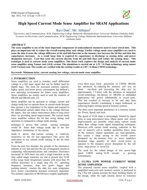
The proposed current sense amplifier, coupled with a<br />
simplified read-cycle-only memory system, is portrayed in<br />
Fig.1.The left column presents the basic building blocks of<br />
the design, while the right column shows its transistor<br />
ISSN: 2250-3021 www.iosrjen.org 1124 | P a g e
IOSR Journal of Engineering<br />
Apr. 2012, Vol. 2(5) pp: 1124-1127<br />
level/circuit structure .The proposed design has integrated<br />
the gist of the conventional current sense amplifier by<br />
including the transistors P 31, P 32, P 33 and P34 operating<br />
in saturation region. Owing to the simulation of this current<br />
conveyor ,the new circuit is intrinsically bit-line<br />
capacitance in sensitive science it has(ideally)zero input<br />
resistance during sensing .It also incorporates a current<br />
amplifier ,made up of two pairs of current mirrors at each<br />
bit-lines, which aims to amplify the bit-line current and<br />
Thus enhancing the sensing speed .Following that, Fig.1<br />
embraces across coupled CMOS amplifier (N 15, N 16, P<br />
45, P 46and N 47)<strong>for</strong> global sensing .<br />
CDL<br />
DL<br />
CDL<br />
DL<br />
Vo<br />
? it-line<br />
load<br />
VDD<br />
Memory<br />
Cell<br />
Memory<br />
Cell<br />
<strong>Current</strong>? conveyor<br />
<strong>Current</strong>? amplifier<br />
VDD<br />
P1<br />
N1<br />
E<br />
E?<br />
N3 ? ¬? 1<br />
N5<br />
? ? Data-lines F<br />
P45 ? ??<br />
Data-linesrequalization<br />
circuit<br />
Fig-1 Ultra Low Power <strong>Current</strong> <strong>Mode</strong> <strong>Sense</strong> <strong>Amplifier</strong><br />
[1]<br />
The complementary signals of the CMOS<br />
amplifier will feed their respective output sections, which<br />
are inverter stages, each cascaded with an additional NMOS<br />
transistor. This Supposedly minor tweak will aid in<br />
minimizing a major proportion of the unnecessary power<br />
dissipation. Data-line equalization is not compulsory in this<br />
circuit due to the inherent equalizing action of transistor N<br />
47. C BL and C DL signify then bit-line and data-line<br />
capacitances, respectively, where as RS and CS denote the<br />
row and column-select. Consider both RS1 and CS2 being<br />
activated during a read operation. The memory cell at the<br />
upper row and right column will be selected, resulting in a<br />
smaller <strong>Current</strong> flow through BL than that at BL. These<br />
0? 6T<br />
VDD<br />
WE<br />
? ?<br />
?L<br />
0? 6T<br />
C ?L<br />
C?L<br />
P21<br />
C<br />
D<br />
N15<br />
N47<br />
? ??<br />
P31<br />
P33<br />
N6<br />
?1<br />
VDD<br />
P22 P23<br />
VDD<br />
P2<br />
N2<br />
Vo<br />
P32<br />
P34<br />
N7<br />
P24<br />
RS1<br />
RS2<br />
CS2<br />
N8<br />
differential current signals that Appear at the common bitlines<br />
will then propagate to two pairs of NMOS current<br />
Mirror (N 5, N 6 and N 7, N 8). In view of the fact that P31,<br />
P 32, P 33and P 34 have to be in saturation mode to ensure<br />
a bit-line capacitance insensitive sensing delay ,the drains<br />
of P 33 and P 34 are pulled to a low-voltage with the aid of<br />
the relatively large-sized N 5 and N8. Mean while, the<br />
widths of N 6 and N 7 are appropriately sized to a smaller<br />
dimension to avoid non essential power wastage. However,<br />
the current mirrors at this stage act as current sink instead<br />
of current source. Two PMOS current mirrors (P 21, P<br />
22and P 23, P 24) are there<strong>for</strong>e included to change the<br />
current direction to comply with our novel design of the<br />
power saving cross-coupled CMOS latch .These two PMOS<br />
current mirrors also double up as current amplifiers, which<br />
serve the purpose of increasing the current transmitted from<br />
the bit-lines by the same amplification ratio. After current<br />
intensification, the bit line currents are considered<br />
adequately large to enhance the sensing speed. Prior to the<br />
read cycle , nodes C and D are clamp data same potentially<br />
the pre-equalizing signal , EQ .This voltage-clamping<br />
signal can only be released after the differential current<br />
from the bit-lines resides at the data-lines to establish a<br />
correct data output .Since the current through P 22 is<br />
smaller than its P 23 counterpart , node E Is charged to a<br />
potential lower than node F(VE
IOSR Journal of Engineering<br />
Apr. 2012, Vol. 2(5) pp: 1124-1127<br />
Fig-2 Voltage Wave <strong>for</strong>ms of <strong>High</strong> <strong>Speed</strong> <strong>Current</strong> <strong>Mode</strong><br />
<strong>Sense</strong> <strong>Amplifier</strong> Circuit<br />
Voltage Signal of <strong>High</strong> <strong>Speed</strong> <strong>Current</strong> <strong>Mode</strong> <strong>Sense</strong><br />
<strong>Amplifier</strong> Circuit at Node - clk<br />
Voltage Signal of <strong>High</strong> <strong>Speed</strong> <strong>Current</strong> <strong>Mode</strong> <strong>Sense</strong><br />
<strong>Amplifier</strong> Circuit at Node – wl<br />
Voltage Signal of <strong>High</strong> <strong>Speed</strong> <strong>Current</strong> <strong>Mode</strong> <strong>Sense</strong><br />
<strong>Amplifier</strong> Circuit at Node - cs<br />
Fig-3 Simulation Wave <strong>for</strong>ms of <strong>High</strong> <strong>Speed</strong> <strong>Current</strong><br />
<strong>Mode</strong> <strong>Sense</strong> <strong>Amplifier</strong> Circuit.<br />
<strong>Current</strong> wave<strong>for</strong>m of <strong>High</strong> <strong>Speed</strong> <strong>Current</strong> <strong>Mode</strong> <strong>Sense</strong><br />
<strong>Amplifier</strong> Circuit at Node – dlb<br />
Voltage wave<strong>for</strong>m of <strong>High</strong> <strong>Speed</strong> <strong>Current</strong> <strong>Mode</strong> <strong>Sense</strong><br />
<strong>Amplifier</strong> Circuit at Node – dlb<br />
Delay wave<strong>for</strong>m of <strong>High</strong> <strong>Speed</strong> <strong>Current</strong> <strong>Mode</strong> <strong>Sense</strong><br />
<strong>Amplifier</strong> Circuit at Node – delay<br />
ISSN: 2250-3021 www.iosrjen.org 1126 | P a g e
IOSR Journal of Engineering<br />
Apr. 2012, Vol. 2(5) pp: 1124-1127<br />
Table-1 Comparison of sensing delay <strong>for</strong> high speed<br />
current mode sense amplifier at CDL = 1PF, Cout = 0.1<br />
PF and CBL varies from 1 Pf of 5 Pf<br />
Bit Line<br />
Capacitance<br />
CBL<br />
(pf)<br />
1<br />
2<br />
3<br />
4<br />
5<br />
Sensing Delay <strong>for</strong><br />
<strong>High</strong> <strong>Speed</strong> <strong>Current</strong> <strong>Mode</strong><br />
<strong>Sense</strong> <strong>Amplifier</strong>(ns)<br />
6.1324e-010<br />
5.9127e-010<br />
5.9317e-010<br />
5.8848e-010<br />
5.8932e-010<br />
The analysis <strong>for</strong> <strong>High</strong> <strong>Speed</strong> <strong>Current</strong> mode <strong>Sense</strong> amplifier<br />
is done at TMSC 0.13um technology node with 1.5V power<br />
supply. The value of sensing delay is calculated <strong>for</strong><br />
combinations of CBL = 1PF, CDL = 1PF Cout = 0.1Pf as<br />
shown in table-1. The analysis shows that the sensing speed<br />
of <strong>High</strong> <strong>Speed</strong> <strong>Current</strong> mode <strong>Sense</strong> amplifier independent<br />
of the variations in bit line capacitances.<br />
REFERENCES<br />
[1] Zhi-Hui Kong, Kiat Seng Yeo, and Chip-Hong<br />
Chang, “An ultra low power current mode sense<br />
amplifier <strong>for</strong> <strong>SRAM</strong> applications”, IEEE Journal of<br />
Circuits, Syst., and Comp. 14, (2005) 939-951.<br />
[2] Yi-Ming Sheng, Ming-Jun Hsiao and Tsin-Yuan<br />
Chang,"A Measurement Unit <strong>for</strong> Input Signal<br />
Analysis of <strong>SRAM</strong> <strong>Sense</strong> <strong>Amplifier</strong>” Proceedings of<br />
the 13th Asian Test Symposium (ATS 2004) 0-7695-<br />
2235-1- 2004 IEEE<br />
[3] Hwang-Cherng Chow and Shu-Hsien Chang," <strong>High</strong><br />
Per<strong>for</strong>mance <strong>Sense</strong> <strong>Amplifier</strong> Circuit <strong>for</strong> Low Power<br />
<strong>SRAM</strong> Applications" Proceedings of the 13th Asian<br />
Test Symposium 0-7803-8251-X-2004 IEEE<br />
[4] Weizhong Wang and Haiyan Gong, “<strong>Sense</strong> <strong>Amplifier</strong><br />
Based RADHARD Flip Flop Design" IEEE<br />
Transactions on Nuclear Science, Vol. 51, No. 6,<br />
December 2004<br />
[5] R. Singh and N. Bhat, “An Offset Compensation<br />
Technique <strong>for</strong> Latch Type <strong>Sense</strong> <strong>Amplifier</strong> in <strong>High</strong>speed<br />
Low-power <strong>SRAM</strong>’s”. IEE Transactions on<br />
VLSI Systems, vol. 12, p. 652.657, June 2004.<br />
[6] Kiat-Seng Yeo, Zhi-Hui Kong, Wang-Ling Goh,<br />
Qingxiang Zhang and Wee-Guan Yeo, “A new<br />
current conveyor amplifier <strong>for</strong> low-voltage high-speed<br />
application”, IEEE, 2003.<br />
[7] Jinn-Shyan Wang and Hong-Yu Lee, “A New<br />
<strong>Current</strong>-<strong>Mode</strong> <strong>Sense</strong> <strong>Amplifier</strong> <strong>for</strong> Low-Voltage<br />
Low-Power <strong>SRAM</strong> Design” 0-7803-4980-<br />
6/98/$10.00 1630 1998-IEEE publishing company,<br />
1990.<br />
3. CONCLUSION<br />
The analysis <strong>for</strong> Conventional <strong>Current</strong> mode <strong>Sense</strong><br />
amplifier is done at TMSC 0.13um technology node with<br />
1.5V power supply. The value of sensing delay is<br />
calculated <strong>for</strong> combinations of CBL = 1PF, CDL = 1PF<br />
Cout = 0.1Pf as shown in table-1.<br />
The analysis shows that the sensing speed of <strong>Current</strong> mode<br />
<strong>Sense</strong> amplifier independent of the variations in bit line<br />
capacitances. It is clear from above table the read delay of<br />
<strong>High</strong> <strong>Speed</strong> <strong>Current</strong> mode <strong>Sense</strong> amplifier is significantly<br />
less as compared to Conventional <strong>Current</strong> mode <strong>Sense</strong><br />
amplifier<br />
ISSN: 2250-3021 www.iosrjen.org 1127 | P a g e