Investigations on Three Phase Five Level Cascaded type ... - IOSRJEN
Investigations on Three Phase Five Level Cascaded type ... - IOSRJEN
Investigations on Three Phase Five Level Cascaded type ... - IOSRJEN
Create successful ePaper yourself
Turn your PDF publications into a flip-book with our unique Google optimized e-Paper software.
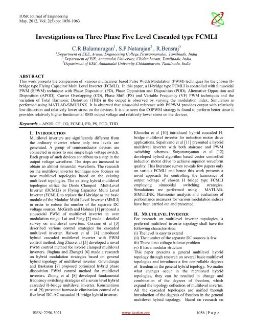
IOSR Journal of EngineeringMay. 2012, Vol. 2(5) pp: 1056-1063hybrid topologies and multicarrier SPWM applied tomultilevel inverter, the paper makes a deep study <strong>on</strong>various modulati<strong>on</strong> strategies applied to hybridtopologies.Fig. 1 shows a c<strong>on</strong>figurati<strong>on</strong> of the three phase fivelevel H bridge <strong>type</strong> FCMLI. The c<strong>on</strong>cept of thisinverter is based <strong>on</strong> c<strong>on</strong>necting H bridge inverters inseries to get a sinusoidal voltage output. The outputvoltage is the sum of the voltage that is generated byeach cell. The number of output voltage levels are2n+1 where n is the number of cells. The switchingangles can be chosen in such a way that the THD isminimized. The output voltage obtained from FCMLIcascade is E/2. An n level cascaded H-bridgemultilevel inverter needs 2(n-1) switching devicesSimilarly for FCMLI cascaded 2(n-1) switchingdevices are used. The gate signals for chosen fivelevel cascaded <strong>type</strong> FCMLI are simulated usingMATLAB-SIMULINK. The gate signal generatordeveloped is tested for various values of modulati<strong>on</strong>index m a and for various PWM strategies. Fig.2shows a sample SIMULINK developed for PDPWMtechnique. The simulati<strong>on</strong> results presented in thispaper in the form of the outputs of the chosen FCMLIcascaded are compared and evaluated.Fig. 1 A three phase five level H-bridge <strong>type</strong> FCMLIFig. 2 Sample PWM generati<strong>on</strong> logic usingSIMULINK developed for PDPWM techniqueIII. MODULATION STRATEGIESDevelopment of c<strong>on</strong>cerns PWM c<strong>on</strong>trol strategies thedevelopment of techniques to reduce the THD of thecurrent. It is generally recognized that increasing theswitching frequency of the PWM pattern reduces thelower frequency harm<strong>on</strong>ics by moving the switchingfrequency carrier harm<strong>on</strong>ics and associated sidebandharm<strong>on</strong>ics further away from the fundamentalfrequency comp<strong>on</strong>ent. The modulating/referencewave of multilevel carrier based PWM strategies canbe sinusoidal. In general for a five level inverter fourcarriers are needed for symmetrical multilevelinverter. As far as the particular reference wave isc<strong>on</strong>cerned, there is also multiple C<strong>on</strong>trol FreedomDegree (CFD) including frequency, amplitude, phaseangle of the reference wave. This paper focuses <strong>on</strong>hybrid power circuit with sinusoidal reference andtriangular carrier which have been used in chosenthree phase cascaded <strong>type</strong> FCMLI. The followingstrategies are employed in this study which have usedthe intersecti<strong>on</strong> of a sine wave with a triangular waveto generate firing pulses.The amplitude modulati<strong>on</strong> index forPD/POD/APOD/VFPWM = 2A m /(m-1)A c.The amplitude modulati<strong>on</strong> index forPSPWM = A m / (A c /2).The amplitude modulati<strong>on</strong> index forCOPWM = A m /(m/4) A C.m f = f c /f mwheref c – Frequency of the carrier signalf m – Frequency of the reference signalA m –Amplitude of the reference signalISSN: 2250-3021 www.iosrjen.org 1057 | P a g e
IOSR Journal of EngineeringMay. 2012, Vol. 2(5) pp: 1056-1063A c – Amplitude of the carrier signalm – number of levels.III. (a) APOD strategyAs can be seen in the Fig.3 for a five level inverter atotal of four carrier waves are used.i) They are arranged in such a manner that eachcarrier is out of phase with its neighbor by 180degrees.ii) The c<strong>on</strong>verter switches to + V dc / 2 when the sinewave is higher than all carrier.iii) The c<strong>on</strong>verter switches to +V dc / 4 when the sinewave is lower than the uppermost carrier waveformand greater than all other carrier.iv) The c<strong>on</strong>verter switches to 0 when the sine wave islower than the two uppermost carrier waveform andgreater than two lowermost carrier.v) The c<strong>on</strong>verter switches to - V dc / 4 when the sinewave is higher than the lowermost carrier waveformand lesser than all other carriers.vi) The c<strong>on</strong>verter switches to - V dc / 2 when the sinewave is lesser than all carrier.e) The c<strong>on</strong>verter switches to - V dc / 4 when the sinewave is higher than the lowermost carrier waveformand lesser than all other carriers.f) The c<strong>on</strong>verter is switched to - V dc / 2 when the sinewave is less than both carrier waveforms.In the PWM scheme there are four triangles, uppertwo triangle have magnitude from 2 to 0 and thelower two triangles exist from 0 to –2 and these twotriangle waveforms are out of phase.Fig. 4 Carrier arrangement for PODPWM strategy(m a = 0.8 and m f = 40)Fig. 3 Carrier arrangement for APODPWM strategy(m a = 0.8 and m f = 40)III. (b) POD strategya) Four carrier waveforms are arranged so that allcarrier waveforms above zero are in phase and are180 degrees out of phase with those below zero.b) The c<strong>on</strong>verter is switched to + V dc / 2 when thesine wave is higher than both carrier waveforms.c)The c<strong>on</strong>verter switches to +V dc / 4 when the sinewave is lower than the uppermost carrier waveformand greater than all other carrier.d) The c<strong>on</strong>verter is switched to zero when the sinewave is greater than the lower carrier waveform butless than the upper carrier waveform.III. (c) PD strategyThe rules for phase dispositi<strong>on</strong> method for amultilevel inverter area) 4 carrier waveforms in phase are arranged.b) The c<strong>on</strong>verter is switched to + V dc / 2 when thesine wave is greater than both carriers.c)The c<strong>on</strong>verter switches to +V dc / 4 when the sinewave is lower than the uppermost carrier waveformand greater than all other carriers.d) The c<strong>on</strong>verter is switched to zero when sine waveis lower than upper carrier but higher than the lowercarrier .e)The c<strong>on</strong>verter switches to - V dc / 4 when the sinewave is higher than the lowermost carrier waveformand lesser than all other carriers.f) The c<strong>on</strong>verter is switched to - V dc / 2 when the sinewave is less than both carrier waveforms.As can be seen from the Fig.5 in the PWM schemethere are four triangles, the upper two trianglesranges from 2 to 0 and the lower two triangle rangesfrom 0 to –2.ISSN: 2250-3021 www.iosrjen.org 1058 | P a g e
IOSR Journal of EngineeringMay. 2012, Vol. 2(5) pp: 1056-1063properly increased to balance the number ofswitchings for all the switches.Fig. 5 Carrier arrangement for PDPWM strategy(m a = 0.8 and m f = 40)III. (d) Carrier Overlapping (CO) strategyFor an m-level inverter using carrier overlappingtechnique, m-1 carriers with the same frequency f cand same peak-to-peak amplitude A c are disposedsuch that the bands they occupy overlap each other;the overlapping vertical distance between each carrieris A c /2. The reference waveform has amplitude of A mand frequency of f m and it is centered in the middle ofthe carrier signals. The reference wave isc<strong>on</strong>tinuously compared with each of the carriersignals. If the reference wave is more than a carriersignal, then the active devices corresp<strong>on</strong>ding to thatcarrier are switched <strong>on</strong>. Otherwise, the devices switchoff.Fig. 7 Carrier arrangement for VFPWM strategy(m a = 0.8 and m f = 40)III. (f) PS strategyThe phase shift multicarrier PWM technique usesfour carrier signals of the same amplitude andfrequency which are shifted by 90 degrees to <strong>on</strong>eanother to generate the five level inverter outputvoltage.Fig.8 Carrier arrangement for PSPWM strategy(m a = 0.8 and m f = 40)Fig. 6 Carrier arrangement for COPWM strategy(m a = 0.8 and m f = 40)III. (e) VF strategyThe number of switchings for upper and lowerdevices of chosen MLI is much more than that ofintermediate switches in PDPWM using c<strong>on</strong>stantfrequency carriers. In order to equalize the number ofswitchings for all the switches, variable frequencyPWM strategy is used as illustrated in which thecarrier frequency of the intermediate switches isIV. SIMULATION RESULTSThe cascaded <strong>type</strong> FCMLI is modeled in SIMULINKusing power system block set. Switching signals forFCMLI are developed using bipolar PWM techniquesdiscussed previously. Simulati<strong>on</strong> is performed fordifferent values of m a ranging from 0.6 – 1. Thecorresp<strong>on</strong>ding %THD values are measured usingFFT block and they are shown in Table 1. Table 2displays the V RMS of fundamental of inverter outputfor same modulati<strong>on</strong> indices. Figs 9-20 show thesimulated output voltage of FCMLI and thecorresp<strong>on</strong>ding FFT plots with above strategies but for<strong>on</strong>ly <strong>on</strong>e sample value of m a = 0.8. Fig.9 shows thefive level output voltage generated by APOD strategyISSN: 2250-3021 www.iosrjen.org 1059 | P a g e
IOSR Journal of EngineeringMay. 2012, Vol. 2(5) pp: 1056-1063and its FFT plot is shown in Fig.10. From Fig.10 it isobserved that the APOD strategy produces significant35 th and 37 th harm<strong>on</strong>ic energy. Fig.11 shows the fivelevel output voltage generated by POD strategy andits FFT plot is shown in Fig.12. From Fig.12 it isobserved that the POD produces significant 33 rd and35 th harm<strong>on</strong>ic energy. Fig.13 shows the five leveloutput voltage generated by PD strategy and its FFTplot is shown in Fig.14. From Fig.14 it is observedthat the PD strategy produces significant 30 th , 32 nd ,36 th and 38 th harm<strong>on</strong>ic energy. Fig.15 shows the fivelevel output voltage generated by CO strategy and itsFFT plot is shown in Fig.16. From Fig.16 it isobserved that the CO strategy produces significant 3 rdand 38 th harm<strong>on</strong>ic energy.Fig.17 shows the five level output voltage generatedby VF strategy and its FFT plot is shown in Fig.18.From Fig.18 it is observed that the VF strategyproduces significant 34 th and 38 th harm<strong>on</strong>ic energy.Fig.19 shows the five level output voltage generatedby PS strategy and its FFT plot is shown in Fig.20.From Fig.20 it is observed that the PS strategy doesnot produce significant harm<strong>on</strong>ic energy. Thefollowing parameter values are used for simulati<strong>on</strong>:V DC =440V, f c = 2KHz and R (load) = 100 ohms.Fig.11 Output voltage generated by PODPWMstrategyFig.12 FFT plot for output voltage of PODPWMstrategyFig.9 Output voltage generated by APODPWMstrategyFig.13 Output voltage generated by PDPWM strategyFig.10 FFT plot for output voltage of APODPWMstrategyFig.14 FFT plot for output voltage of PDPWMstrategyISSN: 2250-3021 www.iosrjen.org 1060 | P a g e
IOSR Journal of EngineeringMay. 2012, Vol. 2(5) pp: 1056-1063Fig.15 Output voltage generated by COPWMstrategyFig.18 FFT plot for output voltage of VFPWMstrategyFig.16 FFT plot for output voltage of COPWMstrategyFig.19 Output voltage generated by PSPWM strategyFig.17 Output voltage generated by VFPWM strategyFig.20 FFT plot for output voltage of PSPWMstrategyTable-1 % THD for different modulati<strong>on</strong> indicesm a PD POD APOD CO VF PS1 27.41 27.33 27.92 32.31 27.44 27.550.9 34.24 34.14 34.65 38.84 34.1 33.420.8 39.18 38.94 39.41 44.16 39.13 39.060.7 42.9 42.71 42.97 55.44 43.31 42.220.6 45.02 45.07 44.95 66.62 45.06 44.91ISSN: 2250-3021 www.iosrjen.org 1061 | P a g e
IOSR Journal of EngineeringMay. 2012, Vol. 2(5) pp: 1056-1063Table-2 V RMS (fundamental) for different modulati<strong>on</strong> indicesm a PD POD APOD CO VF PS1 154.4 154.4 154.2 157.8 154.4 154.50.9 138.6 138.6 138.4 144 138.6 138.80.8 122.7 122.9 122.6 128.9 122.8 122.40.7 106.7 106.5 106.7 110.5 106.4 107.10.6 90.86 90.66 90.91 91.01 91.06 90.11Table-3 Crest factor for different modulati<strong>on</strong> indicesm a PD POD APOD CO VF PS1 1.41386 1.41386 1.414397 1.414449 1.415155 1.4129450.9 1.414141 1.414141 1.414017 1.414583 1.415584 1.4121040.8 1.414018 1.414158 1.414356 1.571761 1.409609 1.4183010.7 1.413308 1.415023 1.414246 1.413575 1.422932 1.4052290.6 1.414264 1.414075 1.414586 1.41413 1.399078 1.429364Table-4 Form factor for different modulati<strong>on</strong> indicesm a PD POD APOD CO VF PS1 199.32 175.5 174.47 10.24 28343.42 140.610.9 150.76 128.09 127.44 7.44 11433.27 151.490.8 86.71 98.08 98.15 6.42 12578.35 111.940.7 105.74 77.11 76.54 4.07 11028.73 87.350.6 75.9 61.92 61.71 2.99 11576.31 64.12V. CONCLUSIONIt is observed from Table 1 PSPWM techniqueprovides output with relatively low distorti<strong>on</strong>.COPWM strategy is found to perform better since itREFERENCES[1] B.P.McGrath and D.G. Holmes, SinusoidalPWM of Multilevel Inverters in theOvermodulati<strong>on</strong> Regi<strong>on</strong>, IEEE Transacti<strong>on</strong>s <strong>on</strong>Industrial Applicati<strong>on</strong>s, Vol.3, No.7, 2002,pp.574-582.[2] J.S.Lai and F.Z.Peng, Multilevel Inverters ASurvey of Topologies, C<strong>on</strong>trols, andApplicati<strong>on</strong>s, IEEE Transacti<strong>on</strong>s <strong>on</strong> IndustrialElectr<strong>on</strong>ics, Vol.49, No.4, 2002, pp.724-738.[3] Keith A. Corzine, Mike W. Wielebski, FangZ. Peng and Jin Wang, C<strong>on</strong>trol of <strong>Cascaded</strong>provides relatively higher fundamental RMS outputvoltage (Table 2) and also relatively lower stress <strong>on</strong>the devices. Table 3 shows crest factor. Next table 4provides FF for all modulati<strong>on</strong> indices.Multilevel Inverter, IEEE Transacti<strong>on</strong>s <strong>on</strong>Power Electr<strong>on</strong>ics, Vol.19, No.3, 2004,pp.732-738.[4] Haiwen Liu, Le<strong>on</strong> M.Tolbert, Surin Khomfoi,Burak Ozpineci and Zh<strong>on</strong>g Du, Hybrid<strong>Cascaded</strong> Multilevel Inverter with PWMC<strong>on</strong>trol Method, IEEE C<strong>on</strong>f. Rec: 978-1-4244-1668-4/08, 2008, pp.162-166.[5] Jing Zhao, Xiangning He and R<strong>on</strong>gxiang Zhao,A Novel PWM C<strong>on</strong>trol Method for Hybrid-Clamped Multilevel Inverters, IEEEISSN: 2250-3021 www.iosrjen.org 1062 | P a g e
IOSR Journal of EngineeringMay. 2012, Vol. 2(5) pp: 1056-1063Transacti<strong>on</strong>s <strong>on</strong> Industrial Electr<strong>on</strong>ics, Vol.57,No.7, 2010, pp.2365-2373.[6] Zhou Jinghua and Li Zhengxi, Research <strong>on</strong>Hybrid Modulati<strong>on</strong> Strategies Based <strong>on</strong>General Hybrid Topology of MultilevelInverter, Internati<strong>on</strong>al Symposium <strong>on</strong> PowerElectr<strong>on</strong>ics Electrical Drives, Automati<strong>on</strong> &Moti<strong>on</strong>, Rec: 978-1-4244-1664-6, 2008,pp.784-788.[7] C.Govindaraju and K.Baskaran, OptimizedHybrid <strong>Phase</strong> Dispositi<strong>on</strong> PWM C<strong>on</strong>trolMethod for Multilevel Inverter, Internati<strong>on</strong>alJournal of Recent Trends in Engineering,Vol.1, No.3, 2009, pp.129-134.[8] Zh<strong>on</strong>g Du, Le<strong>on</strong> M. Tolbert, Burnk Ozpineciand John N. Chiass<strong>on</strong>, Fundamental FrequencySwitching Strategies of a Seven <strong>Level</strong> Hybrid<strong>Cascaded</strong> H-Bridge Multilevel Inverter, IEEETransacti<strong>on</strong>s <strong>on</strong> Power Electr<strong>on</strong>ics, Vol.24,No.1, 2009, pp.25-33.[9] Georgious S. K<strong>on</strong>stantinou, Sridhar R.Pulikantiand Vassilios G. Agelidis, Harm<strong>on</strong>icEliminati<strong>on</strong> C<strong>on</strong>trol of a <strong>Five</strong>-<strong>Level</strong> DC-AC<strong>Cascaded</strong> H-bridge Hybrid Inverter, 2 nd IEEEInternati<strong>on</strong>al Symposium <strong>on</strong> Power Electr<strong>on</strong>icsfor Distributed Generati<strong>on</strong> Systems, 2010,pp.352-357.[10] Farid Khoucha, Soumia Mouna Lagoun,Khoudir Marouani, Abdelaziz Kheloui andMohamed Ei Hachemi Benbouzid, Hybridcascaded H-Bridge Multilevel InverterInducti<strong>on</strong> Motor Drive Direct Torque C<strong>on</strong>trolFor Automotive Applicati<strong>on</strong>s, IEEETransacti<strong>on</strong>s <strong>on</strong> Industrial Electr<strong>on</strong>ics, Vol.57,No.3, 2010, pp.892-899.[11] Hossein Sepahvand, Mostafa Khazraei, MehdiFerdowsi and Keith Corzine, A HybridMultilevel Inverter with Both Staircase andPWM Switching Schemes, IEEE C<strong>on</strong>f. Rec:978-1-4244-5287-3/10, 2010, pp.4364-4367.[12] K.Satyanarayana, J.Amarnath and A.KailasaRao, Hybrid PWM Algorithm Based VectorC<strong>on</strong>trolled Inducti<strong>on</strong> Motor Drive to AchieveSuperior Waveform Quality, Internati<strong>on</strong>alJournal of Engineering & AdvancedTechnology(IJEAT), ISSN:2249-8958, Vol.1,No.2, 2011, pp.56-63.ISSN: 2250-3021 www.iosrjen.org 1063 | P a g e


