TSC2046: Low Voltage I/O Touch Screen Controller (Rev. B)
TSC2046: Low Voltage I/O Touch Screen Controller (Rev. B)
TSC2046: Low Voltage I/O Touch Screen Controller (Rev. B)

You also want an ePaper? Increase the reach of your titles
YUMPU automatically turns print PDFs into web optimized ePapers that Google loves.
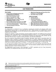
INTERNAL REFERENCE<br />
The <strong>TSC2046</strong> has an internal 2.5V voltage reference that can<br />
be turned on or off with the control bit, PD1 (see Table V and<br />
Figure 3). Typically, the internal reference voltage is only used<br />
in the single-ended mode for battery monitoring, temperature<br />
measurement, and for using the auxiliary input. Optimal touch<br />
screen performance is achieved when using the differential<br />
mode. The internal reference voltage of the <strong>TSC2046</strong> must be<br />
commanded to be off to maintain compatibility with the<br />
ADS7843. Therefore, after power-up, a write of PD1 = 0 is<br />
required to insure the reference is off (see the Typical Characteristics<br />
for power-up time of the reference from powerdown).<br />
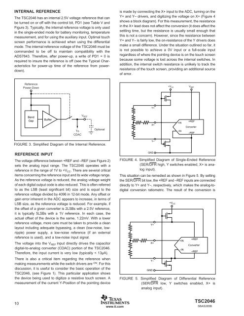
is made by connecting the X+ input to the ADC, turning on the<br />
Y+ and Y– drivers, and digitizing the voltage on X+ (Figure 4<br />
shows a block diagram). For this measurement, the resistance<br />
in the X+ lead does not affect the conversion (it does affect the<br />
settling time, but the resistance is usually small enough that<br />
this is not a concern). However, since the resistance between<br />
Y+ and Y– is fairly low, the on-resistance of the Y drivers does<br />
make a small difference. Under the situation outlined so far, it<br />
is not possible to achieve a 0V input or a full-scale input<br />
regardless of where the pointing device is on the touch screen<br />
because some voltage is lost across the internal switches. In<br />
addition, the internal switch resistance is unlikely to track the<br />
resistance of the touch screen, providing an additional source<br />
of error.<br />
Reference<br />
Power-Down<br />
+V CC V REF<br />
Y+<br />
Band<br />
Gap<br />
Buffer<br />
To<br />
CDAC<br />
V REF<br />
Optional<br />
X+<br />
+IN<br />
–IN<br />
+REF<br />
Converter<br />
–REF<br />
FIGURE 3. Simplified Diagram of the Internal Reference.<br />
Y–<br />
REFERENCE INPUT<br />
The voltage difference between +REF and –REF (see Figure 2)<br />
sets the analog input range. The <strong>TSC2046</strong> operates with a<br />
reference in the range of 1V to +V CC . There are several critical<br />
items concerning the reference input and its wide voltage range.<br />
As the reference voltage is reduced, the analog voltage weight<br />
of each digital output code is also reduced. This is often referred<br />
to as the LSB (least significant bit) size and is equal to the<br />
reference voltage divided by 4096 in 12-bit mode. Any offset or<br />
gain error inherent in the ADC appears to increase, in terms of<br />
LSB size, as the reference voltage is reduced. For example, if<br />
the offset of a given converter is 2LSBs with a 2.5V reference,<br />
it is typically 5LSBs with a 1V reference. In each case, the<br />
actual offset of the device is the same, 1.22mV. With a lower<br />
reference voltage, more care must be taken to provide a clean<br />
layout including adequate bypassing, a clean (low-noise, lowripple)<br />
power supply, a low-noise reference (if an external<br />
reference is used), and a low-noise input signal.<br />
The voltage into the V REF input directly drives the capacitor<br />
digital-to-analog converter (CDAC) portion of the <strong>TSC2046</strong>.<br />
Therefore, the input current is very low (typically < 13µA).<br />
There is also a critical item regarding the reference when<br />
making measurements while the switch drivers are ON . For this<br />
discussion, it is useful to consider the basic operation of the<br />
<strong>TSC2046</strong>, (see Figure 1). This particular application shows<br />
the device being used to digitize a resistive touch screen. A<br />
measurement of the current Y-Position of the pointing device<br />
GND<br />
FIGURE 4. Simplified Diagram of Single-Ended Reference<br />
(SER/DFR high, Y switches enabled, X+ is analog<br />
input).<br />
This situation can be remedied as shown in Figure 5. By setting<br />
the SER/DFR bit low, the +REF and –REF inputs are connected<br />
directly to Y+ and Y–, respectively, which makes the analog-todigital<br />
conversion ratiometric. The result of the conversion is<br />
Y+<br />
X+<br />
Y–<br />
GND<br />
+V CC<br />
Converter<br />
FIGURE 5. Simplified Diagram of Differential Reference<br />
(SER/DFR low, Y switches enabled, X+ is<br />
analog input).<br />
+IN<br />
–IN<br />
+REF<br />
–REF<br />
10<br />
www.ti.com<br />
<strong>TSC2046</strong><br />
SBAS265B