TSC2046: Low Voltage I/O Touch Screen Controller (Rev. B)
TSC2046: Low Voltage I/O Touch Screen Controller (Rev. B)
TSC2046: Low Voltage I/O Touch Screen Controller (Rev. B)

You also want an ePaper? Increase the reach of your titles
YUMPU automatically turns print PDFs into web optimized ePapers that Google loves.
PD1 PD0 PENIRQ DESCRIPTION<br />
0 0 Enabled Power-Down Between Conversions. When each<br />
conversion is finished, the converter enters a<br />
low-power mode. At the start of the next conversion,<br />
the device instantly powers up to full power.<br />
There is no need for additional delays to ensure<br />
full operation, and the very first conversion is<br />
valid. The Y– switch is on when in power-down.<br />
0 1 Disabled Reference is off and ADC is on.<br />
1 0 Enabled Reference is on and ADC is off.<br />
1 1 Disabled Device is always powered. Reference is on and<br />
ADC is ON.<br />
TABLE V. Power-Down and Internal Reference Selection.<br />
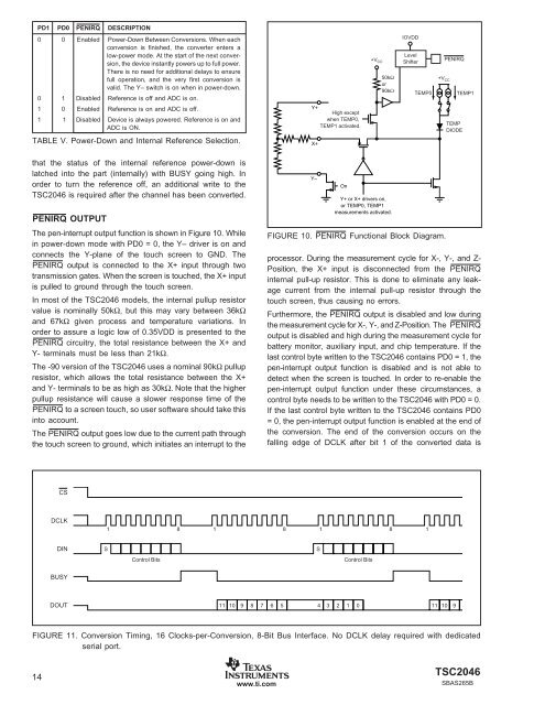
Y+<br />
X+<br />
High except<br />
when TEMP0,<br />
TEMP1 activated.<br />
50kΩ<br />
or<br />
90kΩ<br />
IOVDD<br />
+V CC<br />
Level<br />
Shifter<br />
TEMP0<br />
+V CC<br />
PENIRQ<br />
TEMP<br />
DIODE<br />
TEMP1<br />
that the status of the internal reference power-down is<br />
latched into the part (internally) with BUSY going high. In<br />
order to turn the reference off, an additional write to the<br />
<strong>TSC2046</strong> is required after the channel has been converted.<br />
PENIRQ OUTPUT<br />
Y–<br />
On<br />
Y+ or X+ drivers on,<br />
or TEMP0, TEMP1<br />
measurements activated.<br />
The pen-interrupt output function is shown in Figure 10. While<br />
in power-down mode with PD0 = 0, the Y– driver is on and<br />
connects the Y-plane of the touch screen to GND. The<br />
PENIRQ output is connected to the X+ input through two<br />
transmission gates. When the screen is touched, the X+ input<br />
is pulled to ground through the touch screen.<br />
In most of the <strong>TSC2046</strong> models, the internal pullup resistor<br />
value is nominally 50kΩ, but this may vary between 36kΩ<br />
and 67kΩ given process and temperature variations. In<br />
order to assure a logic low of 0.35VDD is presented to the<br />
PENIRQ circuitry, the total resistance between the X+ and<br />
Y- terminals must be less than 21kΩ.<br />
The -90 version of the <strong>TSC2046</strong> uses a nominal 90kΩ pullup<br />
resistor, which allows the total resistance between the X+<br />
and Y- terminals to be as high as 30kΩ. Note that the higher<br />
pullup resistance will cause a slower response time of the<br />
PENIRQ to a screen touch, so user software should take this<br />
into account.<br />
The PENIRQ output goes low due to the current path through<br />
the touch screen to ground, which initiates an interrupt to the<br />
FIGURE 10. PENIRQ Functional Block Diagram.<br />
processor. During the measurement cycle for X-, Y-, and Z-<br />
Position, the X+ input is disconnected from the PENIRQ<br />
internal pull-up resistor. This is done to eliminate any leakage<br />
current from the internal pull-up resistor through the<br />
touch screen, thus causing no errors.<br />
Furthermore, the PENIRQ output is disabled and low during<br />
the measurement cycle for X-, Y-, and Z-Position. The PENIRQ<br />
output is disabled and high during the measurement cycle for<br />
battery monitor, auxiliary input, and chip temperature. If the<br />
last control byte written to the <strong>TSC2046</strong> contains PD0 = 1, the<br />
pen-interrupt output function is disabled and is not able to<br />
detect when the screen is touched. In order to re-enable the<br />
pen-interrupt output function under these circumstances, a<br />
control byte needs to be written to the <strong>TSC2046</strong> with PD0 = 0.<br />
If the last control byte written to the <strong>TSC2046</strong> contains PD0<br />
= 0, the pen-interrupt output function is enabled at the end of<br />
the conversion. The end of the conversion occurs on the<br />
falling edge of DCLK after bit 1 of the converted data is<br />
CS<br />
DCLK<br />
1<br />
8 1<br />
8 1 8<br />
1<br />
DIN<br />
S<br />
S<br />
Control Bits<br />
Control Bits<br />
BUSY<br />
DOUT<br />
11<br />
10 9 8 7 6 5 4 3 2 1 0 11 10 9<br />
FIGURE 11. Conversion Timing, 16 Clocks-per-Conversion, 8-Bit Bus Interface. No DCLK delay required with dedicated<br />
serial port.<br />
14<br />
www.ti.com<br />
<strong>TSC2046</strong><br />
SBAS265B