ProService Magazine - International Society of Certified Electronics ...
ProService Magazine - International Society of Certified Electronics ...
ProService Magazine - International Society of Certified Electronics ...

Create successful ePaper yourself
Turn your PDF publications into a flip-book with our unique Google optimized e-Paper software.
Exploring Class-D Amplifiers<br />
By David Bates CET, CA<br />
The Class-B or Class-AB amplifier has<br />
been the main choice for many designers <strong>of</strong><br />
audio amplifiers. This linear amplifier configuration<br />
has been able to provide the necessary<br />
conventional performance and cost<br />
requirements. Now, products such as LDC<br />
TVs, plasma TVs, and desktop PCs are driving<br />
the necessity for greater power output<br />
while maintaining or reducing the form-factor,<br />
without increasing costs. Portable powered<br />
devices, such as PDAs, cell phones,<br />
and notebook PCs, are demanding higher<br />
circuit efficiencies. Due to very high efficiency<br />
and low heat dissipation, the Class-D<br />
amplifier is now challenging the Class-AB<br />
amplifiers in many applications.<br />
A Class-D amplifier uses output transistors<br />
operated as switches. This enables the<br />
transistor to either be in a cut<strong>of</strong>f or saturated<br />
mode. When cut<strong>of</strong>f, its current is zero.<br />
When it is saturated, the voltage across it is<br />
low. In each mode, its power dissipation is<br />
very low. This concept increases the circuit<br />
efficiency, therefore, requires less power<br />
from the power supply and enables the use<br />
<strong>of</strong> smaller heat sinks for the amplifier.<br />
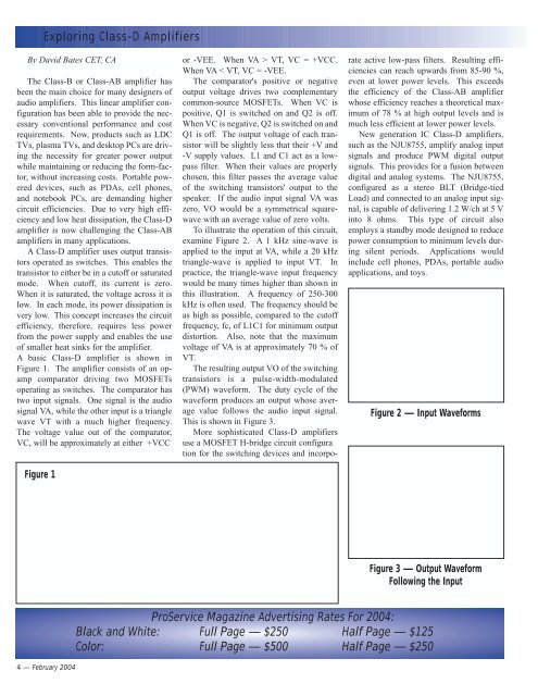
A basic Class-D amplifier is shown in<br />
Figure 1. The amplifier consists <strong>of</strong> an opamp<br />
comparator driving two MOSFETs<br />
operating as switches. The comparator has<br />
two input signals. One signal is the audio<br />
signal VA, while the other input is a triangle<br />
wave VT with a much higher frequency.<br />
The voltage value out <strong>of</strong> the comparator,<br />
VC, will be approximately at either +VCC<br />
Figure 1<br />
or -VEE. When VA > VT, VC = +VCC.<br />
When VA < VT, VC = -VEE.<br />
The comparator's positive or negative<br />
output voltage drives two complementary<br />
common-source MOSFETs. When VC is<br />
positive, Q1 is switched on and Q2 is <strong>of</strong>f.<br />
When VC is negative, Q2 is switched on and<br />
Q1 is <strong>of</strong>f. The output voltage <strong>of</strong> each transistor<br />
will be slightly less that their +V and<br />
-V supply values. L1 and C1 act as a lowpass<br />
filter. When their values are properly<br />
chosen, this filter passes the average value<br />
<strong>of</strong> the switching transistors' output to the<br />
speaker. If the audio input signal VA was<br />
zero, VO would be a symmetrical squarewave<br />
with an average value <strong>of</strong> zero volts.<br />
To illustrate the operation <strong>of</strong> this circuit,<br />
examine Figure 2. A 1 kHz sine-wave is<br />
applied to the input at VA, while a 20 kHz<br />
triangle-wave is applied to input VT. In<br />
practice, the triangle-wave input frequency<br />
would be many times higher than shown in<br />
this illustration. A frequency <strong>of</strong> 250-300<br />
kHz is <strong>of</strong>ten used. The frequency should be<br />
as high as possible, compared to the cut<strong>of</strong>f<br />
frequency, fc, <strong>of</strong> L1C1 for minimum output<br />
distortion. Also, note that the maximum<br />
voltage <strong>of</strong> VA is at approximately 70 % <strong>of</strong><br />
VT.<br />
The resulting output VO <strong>of</strong> the switching<br />
transistors is a pulse-width-modulated<br />
(PWM) waveform. The duty cycle <strong>of</strong> the<br />
waveform produces an output whose average<br />
value follows the audio input signal.<br />
This is shown in Figure 3.<br />
More sophisticated Class-D amplifiers<br />
use a MOSFET H-bridge circuit configura<br />
tion for the switching devices and incorporate<br />
active low-pass filters. Resulting efficiencies<br />
can reach upwards from 85-90 %,<br />
even at lower power levels. This exceeds<br />
the efficiency <strong>of</strong> the Class-AB amplifier<br />
whose efficiency reaches a theoretical maximum<br />
<strong>of</strong> 78 % at high output levels and is<br />
much less efficient at lower power levels.<br />
New generation IC Class-D amplifiers,<br />
such as the NJU8755, amplify analog input<br />
signals and produce PWM digital output<br />
signals. This provides for a fusion between<br />
digital and analog systems. The NJU8755,<br />
configured as a stereo BLT (Bridge-tied<br />
Load) and connected to an analog input signal,<br />
is capable <strong>of</strong> delivering 1.2 W/ch at 5 V<br />
into 8 ohms. This type <strong>of</strong> circuit also<br />
employs a standby mode designed to reduce<br />
power consumption to minimum levels during<br />
silent periods. Applications would<br />
include cell phones, PDAs, portable audio<br />
applications, and toys.<br />
Figure 2 — Input Waveforms<br />
Figure 3 — Output Waveform<br />
Following the Input<br />
4— February 2004<br />
<strong>ProService</strong> <strong>Magazine</strong> Advertising Rates For 2004:<br />
Black and White: Full Page — $250 Half Page — $125<br />
Color: Full Page — $500 Half Page — $250