Click here to view RFM23BP datasheet - HOPE Microelectronics
Click here to view RFM23BP datasheet - HOPE Microelectronics
Click here to view RFM23BP datasheet - HOPE Microelectronics

You also want an ePaper? Increase the reach of your titles
YUMPU automatically turns print PDFs into web optimized ePapers that Google loves.
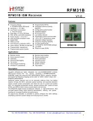
<strong>RFM23BP</strong><br />
<strong>RFM23BP</strong> ISM TRANSCEIVER MODULE<br />
Features<br />
V2.0<br />
• Frequency Range<br />
• 433/868/915MHz ISM bands<br />
• Sensitivity = –120 dBm<br />
• Output power range<br />
• +30 dBm Max (<strong>RFM23BP</strong>)<br />
• Low Power Consumption<br />
• 25 mA receive<br />
• 550 mA @ +30 dBm transmit<br />
• Data Rate = 0.123 <strong>to</strong> 256 kbps<br />
• FSK, GFSK, and OOK modulation<br />
• Power Supply = 3.3 <strong>to</strong> 6 V<br />
• Ultra low power shutdown mode<br />
• Digital RSSI<br />
Applications<br />
• Wake-up timer<br />
• Au<strong>to</strong>-frequency calibration (AFC)<br />
• Power-on-reset (POR)<br />
• Antenna diversity and TR switch<br />
control<br />
• Configurable packet handler<br />
• Preamble detec<strong>to</strong>r<br />
• TX and RX 64 byte FIFOs<br />
• Low battery detec<strong>to</strong>r<br />
• Temperature sensor and 8-bit ADC<br />
• –40 <strong>to</strong> +85 °C temperature range<br />
• Integrated voltage regula<strong>to</strong>rs<br />
• Frequency hopping capability<br />
• On-chip crystal tuning<br />
• 16-PIN SMD package<br />
• Low cost<br />
<strong>RFM23BP</strong><br />
• Remote control<br />
• Home security & alarm<br />
• Telemetry<br />
• Personal data logging<br />
• Toy control<br />
• Tire pressure moni<strong>to</strong>ring<br />
• Wireless PC peripherals<br />
Description<br />
• Remote meter reading<br />
• Remote keyless entry<br />
• Home au<strong>to</strong>mation<br />
• Industrial control<br />
• Sensor networks<br />
• Health moni<strong>to</strong>rs<br />
• Tag readers<br />
HopeRF's <strong>RFM23BP</strong> are highly integrated, low cost,433/868/915MHZ<br />
wireless ISM transceivers module. The low receive sensitivity(–120dBm)<br />
coupled with industry leading +30dBm output power ensures extended<br />
range and improved link performance. Built-in antenna diversity and<br />
support for frequency hopping can be used <strong>to</strong> further extend range and enhance<br />
performance.<br />
Additional system features such as an au<strong>to</strong>matic wake-up timer, low<br />
battery detec<strong>to</strong>r, 64 byte TX/RX FIFOs, au<strong>to</strong>matic packet handling, and preamble<br />
detection reduce overall current consumption and allow the use of lower-cost<br />
system MCUs. An integrated temperature sensor, general purpose ADC, poweron-reset<br />
(POR), and GPIOs further reduce overall system cost and size.<br />
The <strong>RFM23BP</strong> digital receive archit ecture features a high-performance ADC<br />
and DSP based modem which performs demodulation, filtering, and packet<br />
handling for increased flexibility and performance. The direct digital transmit<br />
modulation and au<strong>to</strong>matic PA power ramping ensure precise transmit modulation<br />
and reduced spectral spreading ensuring compliance with global regulations<br />
including FCC, ETSI.<br />
An easy-<strong>to</strong>-use calcula<strong>to</strong>r is provided <strong>to</strong> quickly configure the radio settings,<br />
simplifying cus<strong>to</strong>mer's system design and reducing time <strong>to</strong> market.<br />
1 Tel: +86-755-82973805 Fax: +86-755-82973550 E-mail: sales@hoperf.com http://www.hoperf.com 1
<strong>RFM23BP</strong><br />
TABLE OF C ONTENTS<br />
Section<br />
Page<br />
1. Electrical Specifications . . . . . . . . . . . . . . . . . . . . . . . . . . . . . . . . . . . . . . . . . . . . . . . . . . .4<br />
2. Functional Description . . . . . . . . . . . . . . . . . . . . . . . . . . . . . . . . . . . . . . . . . . . . . . . . . . . 11<br />
2.1. Operating Modes . . . . . . . . . . . . . . . . . . . . . . . . . . . . . . . . . . . . . . . . . . . . . . . . . . . . 13<br />
3. Controller Interface . . . . . . . . . . . . . . . . . . . . . . . . . . . . . . . . . . . . . . . . . . . . . . . . . . . . . . 14<br />
3.1. Serial Peripheral Interface (SPI) . . . . . . . . . . . . . . . . . . . . . . . . . . . . . . . . . . . . . . . . 14<br />
3.2. Operating Mode Control . . . . . . . . . . . . . . . . . . . . . . . . . . . . . . . . . . . . . . . . . . . . . . 16<br />
3.3. Interrupts . . . . . . . . . . . . . . . . . . . . . . . . . . . . . . . . . . . . . . . . . . . . . . . . . . . . . . . . . 19<br />
3.4. System Timing . . . . . . . . . . . . . . . . . . . . . . . . . . . . . . . . . . . . . . . . . . . . . . . . . . . . . 20<br />
3.5. Frequency Control . . . . . . . . . . . . . . . . . . . . . . . . . . . . . . . . . . . . . . . . . . . . . . . . . . . 21<br />
4. Modulation Options . . . . . . . . . . . . . . . . . . . . . . . . . . . . . . . . . . . . . . . . . . . . . . . . . . . . . . 28<br />
4.1. Modulation Type . . . . . . . . . . . . . . . . . . . . . . . . . . . . . . . . . . . . . . . . . . . . . . . . . . . . 28<br />
4.2. Modulation Data Source . . . . . . . . . . . . . . . . . . . . . . . . . . . . . . . . . . . . . . . . . . . . . .29<br />
5. Internal Functional Blocks . . . . . . . . . . . . . . . . . . . . . . . . . . . . . . . . . . . . . . . . . . . . . . . . 33<br />
5.1. RX LNA . . . . . . . . . . . . . . . . . . . . . . . . . . . . . . . . . . . . . . . . . . . . . . . . . . . . . . . . . . . 33<br />
5.2. RX I-Q Mixer . . . . . . . . . . . . . . . . . . . . . . . . . . . . . . . . . . . . . . . . . . . . . . . . . . . . . . . 33<br />
5.3. Programmable Gain Amplifier . . . . . . . . . . . . . . . . . . . . . . . . . . . . . . . . . . . . . . . . . . 33<br />
5.4. ADC . . . . . . . . . . . . . . . . . . . . . . . . . . . . . . . . . . . . . . . . . . . . . . . . . . . . . . . . . . . . . . 33<br />
5.5. Digital Modem . . . . . . . . . . . . . . . . . . . . . . . . . . . . . . . . . . . . . . . . . . . . . . . . . . . . . . 33<br />
5.6. Synthesizer . . . . . . . . . . . . . . . . . . . . . . . . . . . . . . . . . . . . . . . . . . . . . . . . . . . . . . . . 34<br />
5.7. Power Amplifier . . . . . . . . . . . . . . . . . . . . . . . . . . . . . . . . . . . . . . . . . . . . . . . . . . . . . 35<br />
5.8. Crystal Oscilla<strong>to</strong>r . . . . . . . . . . . . . . . . . . . . . . . . . . . . . . . . . . . . . . . . . . . . . . . . . . . . 36<br />
5.9. Regula<strong>to</strong>rs . . . . . . . . . . . . . . . . . . . . . . . . . . . . . . . . . . . . . . . . . . . . . . . . . . . . . . . . . 36<br />
6. Data Handling and Packet Handler . . . . . . . . . . . . . . . . . . . . . . . . . . . . . . . . . . . . . . . . . . 37<br />
6.1. RX and TX FIFOs . . . . . . . . . . . . . . . . . . . . . . . . . . . . . . . . . . . . . . . . . . . . . . . . . . . 37<br />
6.2. Packet Configuration . . . . . . . . . . . . . . . . . . . . . . . . . . . . . . . . . . . . . . . . . . . . . . . . .38<br />
6.3. Packet Handler TX Mode . . . . . . . . . . . . . . . . . . . . . . . . . . . . . . . . . . . . . . . . . . . . .39<br />
6.4. Packet Handler RX Mode . . . . . . . . . . . . . . . . . . . . . . . . . . . . . . . . . . . . . . . . . . . . .39<br />
6.5. Data Whitening, Manchester Encoding, and CRC . . . . . . . . . . . . . . . . . . . . . . . . . . 42<br />
6.6. Preamble Detec<strong>to</strong>r . . . . . . . . . . . . . . . . . . . . . . . . . . . . . . . . . . . . . . . . . . . . . . . . . . 42<br />
6.7. Preamble Length . . . . . . . . . . . . . . . . . . . . . . . . . . . . . . . . . . . . . . . . . . . . . . . . . . . . 43<br />
6.8. Invalid Preamble Detec<strong>to</strong>r . . . . . . . . . . . . . . . . . . . . . . . . . . . . . . . . . . . . . . . . . . . . . 43<br />
6.9. Synchronization Word Configuration . . . . . . . . . . . . . . . . . . . . . . . . . . . . . . . . . . . . . 43<br />
6.10. Receive Header Check . . . . . . . . . . . . . . . . . . . . . . . . . . . . . . . . . . . . . . . . . . . . . . 44<br />
6.11. TX Retransmission and Au<strong>to</strong> TX . . . . . . . . . . . . . . . . . . . . . . . . . . . . . . . . . . . . . . . 44<br />
7. RX Modem Configuration . . . . . . . . . . . . . . . . . . . . . . . . . . . . . . . . . . . . . . . . . . . . . . . . . 45<br />
7.1. Modem Settings for FSK and GFSK . . . . . . . . . . . . . . . . . . . . . . . . . . . . . . . . . . . . . 45<br />
8. Auxiliary Functions . . . . . . . . . . . . . . . . . . . . . . . . . . . . . . . . . . . . . . . . . . . . . . . . . . . . . . 46<br />
8.1. Smart Reset . . . . . . . . . . . . . . . . . . . . . . . . . . . . . . . . . . . . . . . . . . . . . . . . . . . . . . . 46<br />
Tel: +86-755-82973805 Fax: +86-755-82973550<br />
E-mail: sales@hoperf.com http://www.hoperf.com<br />
2
<strong>RFM23BP</strong><br />
8.2. Microcontroller Clock . . . . . . . . . . . . . . . . . . . . . . . . . . . . . . . . . . . . . . . . . . . . . . . . . 47<br />
8.3. General Purpose ADC . . . . . . . . . . . . . . . . . . . . . . . . . . . . . . . . . . . . . . . . . . . . . . .48<br />
8.4. Temperature Sensor . . . . . . . . . . . . . . . . . . . . . . . . . . . . . . . . . . . . . . . . . . . . . . . . .49<br />
8.5. Low Battery Detec<strong>to</strong>r . . . . . . . . . . . . . . . . . . . . . . . . . . . . . . . . . . . . . . . . . . . . . . . . . 51<br />
8.6. Wake-Up Timer and 32 kHz Clock Source . . . . . . . . . . . . . . . . . . . . . . . . . . . . . . . . 52<br />
8.7. Low Duty Cycle Mode . . . . . . . . . . . . . . . . . . . . . . . . . . . . . . . . . . . . . . . . . . . . . . . . 54<br />
8.8. GPIO Configuration . . . . . . . . . . . . . . . . . . . . . . . . . . . . . . . . . . . . . . . . . . . . . . . . . . 55<br />
8.9. Antenna Diversity . . . . . . . . . . . . . . . . . . . . . . . . . . . . . . . . . . . . . . . . . . . . . . . . . . . 56<br />
8.10. RSSI and Clear Channel Assessment . . . . . . . . . . . . . . . . . . . . . . . . . . . . . . . . . . 57<br />
9. Reference Design . . . . . . . . . . . . . . . . . . . . . . . . . . . . . . . . . . . . . . . . . . . . . . . . . . . . . . . .58<br />
10. Register Table and Descriptions . . . . . . . . . . . . . . . . . . . . . . . . . . . . . . . . . . . . . . . . . .59<br />
11. Pin Descriptions: <strong>RFM23BP</strong> . . . . . . . . . . . . . . . . . . . . . . . . . . . . . . . . . . . . . . . . . . . .60<br />
12. Mechanical Dimension:<strong>RFM23BP</strong>. . . . . . . . . . . . . . . . . . . . . . . . . . . . . . . . . . . . . . . . .61<br />
13. Ordering Information.. . . . . . . . . . . . . . . . . . . . . . . . . . . . . . . . . . . . . . . . . . . . . . . . . . . .62<br />
Contact Information . . . . . . . . . . . . . . . . . . . . . . . . . . . . . . . . . . . . . . . . . . . . . . . . . . . . . .62<br />
3<br />
Tel: +86-755-82973805 Fax: +86-755-82973550<br />
E-mail: sales@hoperf.com http://www.hoperf.com
<strong>RFM23BP</strong><br />
1. Electrical Specifications<br />
Table 1. DC Characteristics<br />
Parameter Symbol Conditions Min Typ Max Units<br />
Supply Voltage Range V DD 3.3 5 6 V<br />
Power Saving Modes<br />
I Shutdown<br />
I Standby<br />
I Sleep<br />
I Sensor-LBD<br />
I Sensor-TS<br />
I Ready<br />
RC Oscilla<strong>to</strong>r, Main Digital Regula<strong>to</strong>r,<br />
and Low Power Digital Regula<strong>to</strong>r OFF<br />
Low Power Digital Regula<strong>to</strong>r ON (Register values retained)<br />
and Main Digital Regula<strong>to</strong>r, and RC Oscilla<strong>to</strong>r OFF<br />
RC Oscilla<strong>to</strong>r and Low Power Digital Regula<strong>to</strong>r ON<br />
(Register values retained) and Main Digital Regula<strong>to</strong>r OFF<br />
Main Digital Regula<strong>to</strong>r and Low Battery Detec<strong>to</strong>r ON,<br />
Crystal Oscilla<strong>to</strong>r and all other blocks OFF<br />
Main Digital Regula<strong>to</strong>r and Temperature Sensor ON,<br />
Crystal Oscilla<strong>to</strong>r and all other blocks OFF<br />
Crystal Oscilla<strong>to</strong>r and Main Digital Regula<strong>to</strong>r ON,<br />
all other blocks OFF. Crystal Oscilla<strong>to</strong>r buffer disabled<br />
— 15 50 nA<br />
— 450 800 nA<br />
— 1 — µA<br />
— 1 — µA<br />
— 1 — µA<br />
— 800 — µA<br />
TUNE Mode Current I Tune Synthesizer and regula<strong>to</strong>rs enabled — 8.5 — mA<br />
RX Mode Current I RX — 25 — mA<br />
TX Mode Current<br />
—<strong>RFM23BP</strong><br />
I TX_+Max txpow[2:0] = 110 (+30 dBm)<br />
— 550 — mA<br />
I TX_+Min<br />
txpow[2:0] = 001 (TBD dBm) — TBD — mA<br />
Tel: +86-755-82973805 Fax: +86-755-82973550 E-mail: sales@hoperf.com http://www.hoperf.com<br />
4<br />
- 4 -
<strong>RFM23BP</strong><br />
Table 2. Synthesizer AC Electrical Characteristics<br />
Parameter Symbol Conditions Min Typ Max Units<br />
Synthesizer Frequency<br />
Range—<strong>RFM23BP</strong><br />
F SYN<br />
433MHz band<br />
868MHz band<br />
915MHz band<br />
413<br />
848<br />
901<br />
453<br />
888<br />
929<br />
MHz<br />
MHZ<br />
MHz<br />
Synthesizer Frequency<br />
Resolution<br />
F RES-LB 433MHz Band — 156.25 — Hz<br />
F RES-HB 868/915MHz Band — 312.5 — Hz<br />
Reference Frequency<br />
Input Level<br />
f REF_LV<br />
When using external reference signal<br />
driving XOUT pin, instead of using<br />
crystal. Measured peak-<strong>to</strong>-peak (V PP )<br />
0.7 — 1.6 V<br />
Synthesizer Settling Time t LOCK Measured from exiting Ready mode with<br />
XOSC running <strong>to</strong> any frequency.<br />
Including VCO Calibration.<br />
Residual FM ΔF RMS Integrated over ±250 kHz bandwidth<br />
(500 Hz lower bound of integration)<br />
— 200 — µs<br />
— 2 4 kHz RMS<br />
Phase Noise<br />
Lφ(f M ) ΔF = 10 kHz — –80 — dBc/Hz<br />
ΔF = 100 kHz — –90 — dBc/Hz<br />
ΔF = 1 MHz — –115 — dBc/Hz<br />
ΔF = 10 MHz — –130 — dBc/Hz<br />
Tel: +86-755-82973805 Fax: +86-755-82973550 E-mail: sales@hoperf.com http://www.hoperf.com
Table 3. Receiver AC Electrical Characteristics<br />
- 6 -<br />
<strong>RFM23BP</strong><br />
Parameter Symbol Conditions Min Typ Max Units<br />
RX Frequency<br />
Range—<strong>RFM23BP</strong><br />
RX Sensitivity<br />
433MHz band<br />
F RX<br />
868MHz band<br />
915MHz band<br />
P RX_2 (BER < 0.1%)<br />
(2 kbps, GFSK, BT = 0.5, Δf = ± 5 kHz)<br />
special crystal is used on the module<br />
P RX_40 (BER < 0.1%)<br />
(1.2 kbps, FSK, BT=0.5,<br />
Δf = ±45kHz)<br />
P RX_100 (BER < 0.1%)<br />
(100 kbps, GFSK, BT = 0.5,<br />
Δf = ±50 kHz)<br />
P RX_125 (BER < 0.1%)<br />
(125 kbps, GFSK, BT = 0.5,<br />
Δf = ±62.5 kHz)<br />
(BER < 0.1%)<br />
(4.8 kbps, 350 kHz BW, OOK)<br />
(BER < 0.1%)<br />
(40 kbps, 400 kHz BW, OOK)<br />
P RX_OOK<br />
413<br />
848<br />
895<br />
453<br />
888<br />
935<br />
MHz<br />
MHz<br />
MHz<br />
— –120 — dBm<br />
— –114 — dBm<br />
— –104 — dBm<br />
— –101 — dBm<br />
— –110 — dBm<br />
— –102 — dBm<br />
RX Channel Bandwidth BW 2.6 — 620 kHz<br />
BER Variation vs Power<br />
Level<br />
P RX_RES Up <strong>to</strong> +5 dBm Input Level — 0 0.1 ppm<br />
RSSI Resolution RES RSSI — ±0.5 — dB<br />
±1-Ch Offset Selectivity C/I 1-CH Desired Ref Signal 3 dB above sensitivity, — –31 — dB<br />
±2-Ch Offset Selectivity C/I<br />
BER < 0.1%. Interferer and desired modu-<br />
2-CH — –35 — dB<br />
lated with 40 kbps ΔF = 20 kHz GFSK with<br />
≥ ±3-Ch Offset Selectivity C/I 3-CH BT = 0.5, channel spacing = 150 kHz<br />
— –40 — dB<br />
Blocking at 1 MHz Offset 1M BLOCK Desired Ref Signal 3 dB above sensitivity. — –52 — dB<br />
Blocking at 4 MHz Offset 4M<br />
Interferer and desired modulated with<br />
BLOCK — –56 — dB<br />
40 kbps ΔF = 20 kHz GFSK with BT = 0.5<br />
Blocking at 8 MHz Offset 8M BLOCK<br />
— –63 — dB<br />
Image Rejection Im REJ Rejection at the image frequency. — –30 — dB<br />
IF=937 kHz<br />
Spurious Emissions P OB_RX1 Measured at RX pins — — –54 dBm<br />
Tel: +86-755-82973805 Fax: +86-755-82973550 E-mail: sales@hoperf.com http://www.hoperf.com<br />
6
<strong>RFM23BP</strong><br />
Table 4. Transmitter AC Electrical Characteristics<br />
Parameter Symbol Conditions Min Typ Max Units<br />
TX Frequency<br />
Range—<strong>RFM23BP</strong><br />
F TX<br />
433MHz band<br />
868MHz band<br />
915MHz band<br />
413<br />
848<br />
895<br />
453<br />
888<br />
935<br />
MHz<br />
MHz<br />
MHz<br />
FSK Data Rate DR FSK 0.123 — 256 kbps<br />
OOK Data Rate DR OOK 0.123 — 40 kbps<br />
Modulation Deviation<br />
Modulation Deviation<br />
Resolution<br />
Output Power<br />
Range—<strong>RFM23BP</strong><br />
Δf1 868/915MHz ±0.625 ±320 kHz<br />
Δf2 433MHz ±0.625 ±160 kHz<br />
Δf RES — 0.625 — kHz<br />
P TX — +30 — dBm<br />
TX RF Output Steps ΔP RF_OUT controlled by txpow[2:0] — 3 — dB<br />
TX RF Output Level<br />
Variation vs. Temperature<br />
TX RF Output Level<br />
Variation vs. Frequency<br />
Transmit Modulation<br />
Filtering<br />
Spurious Emissions<br />
ΔP RF_TEMP –40 <strong>to</strong> +85 °C — 2 — dB<br />
ΔP RF_FREQ<br />
B*T<br />
P OB-TX1<br />
Measured across any one<br />
frequency band<br />
Gaussian Filtering Bandwith Time<br />
Product<br />
P OUT = +30 dBm,<br />
Frequencies
<strong>RFM23BP</strong><br />
Table 5. Auxiliary Block Specifications<br />
Parameter Symbol Conditions Min Typ Max Units<br />
Temperature Sensor<br />
Accuracy<br />
Temperature Sensor<br />
Sensitivity<br />
Low Battery Detec<strong>to</strong>r<br />
Resolution<br />
Low Battery Detec<strong>to</strong>r<br />
Conversion Time<br />
Microcontroller Clock<br />
Output Frequency<br />
General Purpose ADC<br />
Resolution<br />
General Purpose ADC Bit<br />
Resolution<br />
Temp Sensor & General<br />
Purpose ADC Conversion<br />
Time<br />
TS A<br />
After calibrated via sensor offset<br />
register tvoffs[7:0]<br />
— 0.5 — °C<br />
TS S — 5 — mV/°C<br />
LBD RES — 50 — mV<br />
LBD CT — 250 — µs<br />
F MC<br />
Configurable <strong>to</strong> 30 MHz,<br />
15 MHz, 10 MHz, 4 MHz,<br />
3 MHz, 2 MHz, 1 MHz, or<br />
32.768 kHz<br />
32.768K — 30M Hz<br />
ADC ENB — 8 — bit<br />
ADC RES — 4 — mV/bit<br />
ADC CT — 305 — µs<br />
30 MHz XTAL Start-Up time t 30M — 600 — µs<br />
30 MHz XTAL Cap<br />
Resolution<br />
30M RES — 97 — fF<br />
32 kHz XTAL Start-Up Time t 32k — 6 — sec<br />
32 kHz XTAL Accuracy<br />
using 32 kHz XTAL<br />
32 kHz Accuracy using<br />
Internal RC Oscilla<strong>to</strong>r<br />
32K RES<br />
— 100 — ppm<br />
32KRC RES — 2500 — ppm<br />
POR Reset Time t POR — 16 — ms<br />
Software Reset Time t soft — 100 — µs<br />
Tel: +86-755-82973805 Fax: +86-755-82973550 E-mail: sales@hoperf.com http://www.hoperf.com<br />
8
<strong>RFM23BP</strong><br />
Table 6. Digital IO Specifications (SDO, SDI, SCLK, nSEL, and nIRQ)<br />
Parameter Symbol Conditions Min Typ Max Units<br />
Rise Time T RISE 0.1 x V DD <strong>to</strong> 0.9 x V DD , C L = 5 pF — — 8 ns<br />
Fall Time T FALL 0.9 x V DD <strong>to</strong> 0.1 x V DD, C L = 5 pF — — 8 ns<br />
Input Capacitance C IN — — 1 pF<br />
Logic High Level Input Voltage V IH V DD – 0.6 — — V<br />
Logic Low Level Input Voltage V IL — 0.6 V<br />
Input Current I IN 0
<strong>RFM23BP</strong><br />
Table 8. Absolute Maximum Ratings<br />
Parameter Value Unit<br />
V DD <strong>to</strong> GND –0.3, +8.3 V<br />
Instantaneous V RF-peak <strong>to</strong> GND on TX Output Pin –0.3, +8.3 V<br />
Sustained V RF-peak <strong>to</strong> GND on TX Output Pin –0.3, +8.3 V<br />
Voltage on Digital Control Inputs –0.3, V DD + 0.3 V<br />
Voltage on Analog Inputs –0.3, V DD + 0.3 V<br />
RX Input Power +10 dBm<br />
Operating Temperature Range (special crystal is used on the module) T S –40 <strong>to</strong> +85 °C<br />
Operating Temperature Range (Normal crystal is used on the module) T N –20 <strong>to</strong> +60 °C<br />
Thermal Impedance θ JA 30 °C/W<br />
S<strong>to</strong>rage Temperature Range T STG –55 <strong>to</strong> +125 °C<br />
Note: Stresses beyond those listed under “Absolute Maximum Ratings” may cause permanent damage <strong>to</strong> the device. These<br />
are stress ratings only and functional operation of the device at or beyond these ratings in the operational sections of<br />
the specifications is not implied. Exposure <strong>to</strong> absolute maximum rating conditions for extended periods may affect<br />
device reliability. Power Amplifier may be damaged if switched on without proper load or termination connected. TX<br />
matching network design will influence TX V RF-peak on TX output pin. Caution: ESD sensitive device.<br />
Tel: +86-755-82973805 Fax: +86-755-82973550 E-mail: sales@hoperf.com http://www.hoperf.com<br />
10
<strong>RFM23BP</strong><br />
2. Functional Description<br />
HopeRF's <strong>RFM23BP</strong> are highly integrated,low cost,433/868/915MHz wireless ISM transceivers module .<br />
The wide operating voltage range of 3.3–6V and low current consumption makes the<strong>RFM23BP</strong><br />
an ideal solution for battery powered applications.<br />
The <strong>RFM23BP</strong> operates as a time division duplexing (TDD) transceiver w<strong>here</strong> the device alternately transmits<br />
and receives data packets. The device uses a single-conversion mixer <strong>to</strong> downconvert the 2-level FSK/GFSK/OOK<br />
modulated receive signal <strong>to</strong> a low IF frequency. Following a programmable gain amplifier (PGA) the signal is<br />
converted <strong>to</strong> the digital domain by a high performance ΔΣ ADC allowing filtering, demodulation, slicing, and packet<br />
handling <strong>to</strong> be performed in the built-in DSP increasing the receiver’s performance and flexibility versus analog<br />
based architectures. The demodulated signal is then output <strong>to</strong> the system MCU through a programmable GPIO or<br />
via the standard SPI bus by reading the 64-byte RX FIFO.<br />
A single high precision local oscilla<strong>to</strong>r (LO) is used for both transmit and receive modes since the transmitter and<br />
receiver do not operate at the same time. The LO is generated by an integrated VCO and ΔΣ Fractional-N PLL<br />
synthesizer. The synthesizer is designed <strong>to</strong> support configurable data rates, output frequency and frequency<br />
deviation at 433MHz,868MHz,915MHz band. The transmit FSK data is modulated directly in<strong>to</strong> the ΔΣ data<br />
stream and can be shaped by a Gaussian low-pass filter <strong>to</strong> reduce unwanted spectral content.<br />
The <strong>RFM23BP</strong> PA output power can be configured between +10 and +30 dBm ,. The <strong>RFM23BP</strong> supports<br />
frequency hopping, TX/RX switch control, and antenna diversity switch control <strong>to</strong> extend the link range and<br />
improve performance The <strong>RFM23BP</strong> is designed <strong>to</strong> work with a microcontroller <strong>to</strong> create a very low cost<br />
system as shown Figure 1. Voltage regula <strong>to</strong>rs are integrated on-chip which allows for a wide operating<br />
supply voltage range from +3.3<strong>to</strong> +6 V. A standard 4-pin SPI bus is used <strong>to</strong> communicate with an external<br />
microcontroller. Three configurable general purpose I/Os are available. A complete list of the available GPIO<br />
functions is shown in<br />
"8. Auxiliary Functions"and includes microcontroller clock output, Antenna Diversity, POR, and various interrupts.<br />
Tel: +86-755-82973805 Fax: +86-755-82973550 E-mail: sales@hoperf.com http://www.hoperf.com<br />
11
2.1. Operating Modes<br />
<strong>RFM23BP</strong><br />
The <strong>RFM23BP</strong> provides several operating modes which can be used <strong>to</strong> optimize the power consumption for a<br />
given application. Depending upon the system communication pro<strong>to</strong>col, an optimal trade-off between the radio<br />
wake time and power consumption can be achieved.<br />
Table 9 summarizes the operating modes of the <strong>RFM23BP</strong>. In general, any given operating mode may be<br />
classified as an active mode or a power saving mode. The table indicates which block(s) are enabled (active) in<br />
each corresponding mode. With the exception of the SHUTDOWN mode, all can be dynamically selected by<br />
sending the appropriate commands over the SPI. An “X” in any cell means that, in the given mode of operation,<br />
that block can be independently programmed <strong>to</strong> be either ON or OFF, without noticeably impacting the current<br />
consumption. The SPI circuit block includes the SPI interface hardware and the device register space. The 32 kHz<br />
OSC block includes the 32.768 kHz RC oscilla<strong>to</strong>r or 32.768 kHz crystal oscilla<strong>to</strong>r and wake-up timer. AUX<br />
(Auxiliary Blocks) includes the temperature sensor, general purpose ADC, and low-battery detec<strong>to</strong>r.<br />
Table 9. Operating Modes<br />
Mode<br />
Name<br />
Circuit Blocks<br />
Digital LDO SPI 32 kHz OSC AUX 30 MHz<br />
XTAL<br />
PLL PA RX I VDD<br />
SHUT-<br />
DOWN<br />
OFF (Register<br />
contents lost)<br />
OFF OFF OFF OFF OFF OFF OFF 15 nA<br />
STANDBY ON (Register ON OFF OFF OFF OFF OFF OFF 450 nA<br />
SLEEP<br />
contents<br />
retained) ON ON X OFF OFF OFF OFF 1 µA<br />
SENSOR ON X ON OFF OFF OFF OFF 1 µA<br />
READY ON X X ON OFF OFF OFF 800 µA<br />
TUNING ON X X ON ON OFF OFF 8.5 mA<br />
TRANSMIT ON X X ON ON ON OFF 550mA*<br />
RECEIVE<br />
ON X X ON ON OFF ON 18.5 mA<br />
*Note: Using <strong>RFM23BP</strong> at +30 dBm using recommended reference design.<br />
Tel: +86-755-82973805 Fax: +86-755-82973550 E-mail: sales@hoperf.com http://www.hoperf.com<br />
13
<strong>RFM23BP</strong><br />
3. Controller Interface<br />
3.1. Serial Peripheral Interface (SPI)<br />
The <strong>RFM23BP</strong> communicates with the host MCU over a standard 3-wire SPI interface: SCLK, SDI, and nSEL.<br />
The host MCU can read data from the device on the SDO output pin. A SPI transaction is a 16-bit sequence which<br />
consists of a Read-Write (R/W) select bit, followed by a 7-bit address field (ADDR), and an 8-bit data field (DATA)<br />
as demonstrated in Figure 3. The 7-bit address field is used <strong>to</strong> select one of the 128, 8-bit control registers. The<br />
R/W select bit determines whether the SPI transaction is a read or write transaction. If R/W = 1 it signifies a WRITE<br />
transaction, while R/W = 0 signifies a READ transaction. The contents (ADDR or DATA) are latched in<strong>to</strong> the<br />
<strong>RFM23BP</strong> every eight clock cycles. The timing parameters for the SPI interface are shown in Table 10. The<br />
SCLK rate is flexible with a maximum rate of 10 MHz.<br />
SDI<br />
Address<br />
Data<br />
MSB<br />
LSB<br />
RW A6 A5 A4 A3 A2 A1 A0 D7 D6 D5 D4 D3 D2 D1 D0 xx xx RW A7<br />
SCLK<br />
nSEL<br />
Figure 3. SPI Timing<br />
Table 10. Serial Interface Timing Parameters<br />
Symbol Parameter Min (nsec) Diagram<br />
t CH Clock high time 40<br />
t CL Clock low time 40<br />
t DS Data setup time 20<br />
t DH Data hold time 20<br />
t DD Output data delay time 20<br />
t EN Output enable time 20<br />
t DE Output disable time 50<br />
t SS Select setup time 20<br />
t SH Select hold time 50<br />
t SW Select high period 80<br />
SCLK<br />
SDI<br />
SDO<br />
nSEL<br />
tSS tCL tCH tDS tDH tDD tSH tDE<br />
t EN<br />
t SW<br />
To read back data from the <strong>RFM23BP</strong>, the R/W bit must be set <strong>to</strong> 0 followed by the 7-bit address of the register<br />
from which <strong>to</strong> read. The 8 bit DATA field following the 7-bit ADDR field is ignored on the SDI pin when R/W = 0. The<br />
next eight negative edge transitions of the SCLK signal will clock out the contents of the selected register. The data<br />
read from the selected register will be available on the SDO output pin. The READ function is shown in Figure 4.<br />
After the READ function is completed the SDO pin will remain at either a logic 1 or logic 0 state depending on the<br />
last data bit clocked out (D0). When nSEL goes high the SDO output pin will be pulled high by internal pullup.<br />
14<br />
Tel: +86-755-82973805 Fax: +86-755-82973550 E-mail: sales@hoperf.com http://www.hoperf.com
<strong>RFM23BP</strong><br />
SDI<br />
First Bit<br />
RW<br />
=0<br />
A6 A5 A4 A3 A2 A1 A0<br />
D7<br />
=X<br />
D6<br />
=X<br />
D5<br />
=X<br />
D4<br />
=X<br />
D3<br />
=X<br />
D2<br />
=X<br />
D1<br />
=X<br />
Last Bit<br />
D0<br />
=X<br />
SCLK<br />
First Bit<br />
SDO D7 D6 D5 D4 D3 D2 D1 D0<br />
Last Bit<br />
nSEL<br />
Figure 4. SPI Timing—READ Mode<br />
The SPI interface contains a burst read/write mode which allows for reading/writing sequential registers without<br />
having <strong>to</strong> re-send the SPI address. When the nSEL bit is held low while continuing <strong>to</strong> send SCLK pulses, the SPI<br />
interface will au<strong>to</strong>matically increment the ADDR and read from/write <strong>to</strong> the next address. An example burst write<br />
transaction is illustrated in Figure 5 and a burst read in Figure 6. As long as nSEL is held low, input data will be<br />
latched in<strong>to</strong> the <strong>RFM23BP</strong> every eight SCLK cycles.<br />
SDI<br />
First Bit<br />
RW<br />
=1<br />
A6 A5 A4 A3 A2 A1 A0<br />
D7<br />
=X<br />
D6<br />
=X<br />
D5<br />
=X<br />
D4<br />
=X<br />
D3<br />
=X<br />
D2<br />
=X<br />
D1<br />
=X<br />
D0<br />
=X<br />
D7<br />
=X<br />
D6<br />
=X<br />
D5<br />
=X<br />
D4 D3 D2 D1<br />
=X =X =X =X<br />
Last Bit<br />
D0<br />
=X<br />
SCLK<br />
nSEL<br />
Figure 5. SPI Timing—Burst Write Mode<br />
First Bit<br />
Last Bit<br />
SDI<br />
RW<br />
=0<br />
A6 A5 A4 A3 A2 A1 A0<br />
D7<br />
=X<br />
D6<br />
=X<br />
D5<br />
=X<br />
D4<br />
=X<br />
D3<br />
=X<br />
D2<br />
=X<br />
D1<br />
=X<br />
D0<br />
=X<br />
SCLK<br />
SDO<br />
First Bit<br />
D7 D6 D5 D4 D3 D2 D1 D0 D7 D6 D5 D4 D3 D2 D1 D0<br />
nSEL<br />
Figure 6. SPI Timing—Burst Read Mode<br />
Tel: +86-755-82973805 Fax: +86-755-82973550 E-mail: sales@hoperf.com http://www.hoperf.com 15
<strong>RFM23BP</strong><br />
3.2. Operating Mode Control<br />
T<strong>here</strong> are four primary states in the <strong>RFM23BP</strong> radio state machine:SHUTDOWN, IDLE, TX, and RX (see<br />
Figure 7). The SHUTDOWN state completely shuts down the radio <strong>to</strong> minimize current consumption. T<strong>here</strong> are five<br />
different configurations/options for the IDLE state which can be selected <strong>to</strong> optimize the chip <strong>to</strong> the applications<br />
needs. "Register 07h. Operating Mode and Function Control 1" controls which operating mode/state is selected<br />
with the exception of SHUTDOWN which is controlled by SDN pin 20. The TX and RX state may be reached<br />
au<strong>to</strong>matically from any of the IDLE states by setting the txon/rxon bits in "Register 07h. Operating Mode and<br />
Function Control 1". Table 11 shows each of the operating modes with the time required <strong>to</strong> reach either RX or TX<br />
mode as well as the current consumption of each mode.<br />
The <strong>RFM23BP</strong> includes a low-power digital regulated supply (LPLDO) which is internally connected in parallel <strong>to</strong><br />
the output of the main digital regula<strong>to</strong>r (and is available externally at the VR_DIG pin). This common digital<br />
supply voltage is connected <strong>to</strong> all digital circuit blocks including the digital modem, crystal oscilla<strong>to</strong>r, SPI, and<br />
register space. The LPLDO has extremely low quiescent current consumption but limited current supply capability;<br />
it is used only in the IDLE-STANDBY and IDLE-SLEEP modes. The main digital regula<strong>to</strong>r is au<strong>to</strong>matically enabled<br />
in all other modes.<br />
SSHHUUTDDOWWNN<br />
LEID*<br />
TX<br />
*Five Different Options for IDLE<br />
Figure 7. State Machine Diagram<br />
Table 11. Operating Modes Response Time<br />
RX<br />
State/Mode<br />
Response Time <strong>to</strong><br />
TX<br />
RX<br />
Current in State /Mode<br />
[µA]<br />
Shut Down State 16.8 ms 16.8 ms 15 nA<br />
Idle States:<br />
Standby Mode<br />
Sleep Mode<br />
Sensor Mode<br />
Ready Mode<br />
Tune Mode<br />
800 µs<br />
800 µs<br />
800 µs<br />
200 µs<br />
200 µs<br />
800 µs<br />
800 µs<br />
800 µs<br />
200 µs<br />
200 µs<br />
450 nA<br />
1 µA<br />
1 µA<br />
800 µA<br />
8.5 mA<br />
TX State NA 200 µs 550 mA @ +30 dBm<br />
RX State 200 µs NA 18.5 mA<br />
16<br />
Tel: +86-755-82973805 Fax: +86-755-82973550 E-mail: sales@hoperf.com http://www.hoperf.com
<strong>RFM23BP</strong><br />
3.2.1. SHUTDOWN State<br />
The SHUTDOWN state is the lowest current consumption state of the device with nominally less than 15 nA of<br />
current consumption. The shutdown state may be entered by driving the SDN pin high. The SDN pin<br />
should be held low in all states except the SHUTDOWN state. In the SHUTDOWN state, the contents of the<br />
registers are lost and t<strong>here</strong> is no SPI access.<br />
When the chip is connected <strong>to</strong> the power supply, a POR will be initiated after the falling edge of SDN.<br />
3.2.2. IDLE State<br />
T<strong>here</strong> are five different modes in the IDLE state which may be selected by "Register 07h. Operating Mode and<br />
Function Control 1". All modes have a tradeoff between current consumption and response time <strong>to</strong> TX/RX mode.<br />
This tradeoff is shown in Table 11. After the POR event, SWRESET, or exiting from the SHUTDOWN state the chip<br />
will default <strong>to</strong> the IDLE-READY mode. After a POR event the interrupt registers must be read <strong>to</strong> properly enter the<br />
SLEEP, SENSOR, or STANDBY mode and <strong>to</strong> control the 32 kHz clock correctly.<br />
3.2.2.1. STANDBY Mode<br />
STANDBY mode has the lowest current consumption of the five IDLE states with only the LPLDO enabled <strong>to</strong><br />
maintain the register values. In this mode the registers can be accessed in both read and write mode. The<br />
STANDBY mode can be entered by writing 0h <strong>to</strong> "Register 07h. Operating Mode and Function Control 1". If an<br />
interrupt has occurred (i.e., the nIRQ pin = 0) the interrupt registers must be read <strong>to</strong> achieve the minimum current<br />
consumption. Additionally, the ADC should not be selected as an input <strong>to</strong> the GPIO in this mode as it will cause<br />
excess current consumption.<br />
3.2.2.2. SLEEP Mode<br />
In SLEEP mode the LPLDO is enabled along with the Wake-Up-Timer, which can be used <strong>to</strong> accurately wake-up<br />
the radio at specified intervals. See "8.6. Wake-Up Timer and 32 kHz Clock Source for more information<br />
on the Wake -Up-Timer. SLEEP mode is entered by setting enwt = 1 (40h) in "Register 07h. Operating<br />
Mode and Function Control 1". If an interrupt has occurred (i.e., the nIRQ pin = 0) the interrupt registers must be<br />
read <strong>to</strong> achieve the minimum current consumption. Also, the ADC should not be selected as an input <strong>to</strong> the GPIO<br />
in this mode as it will cause excess current consumption.<br />
3.2.2.3. SENSOR Mode<br />
In SENSOR mode either the Low Battery Detec<strong>to</strong>r, Temperature Sensor, or both may be enabled in addition <strong>to</strong> the<br />
LPLDO and Wake-Up-Timer. The Low Battery Detec<strong>to</strong>r can be enabled by setting enlbd = 1 in "Register 07h.<br />
Operating Mode and Function Control 1". See "8.4. Temperature Sensor" and "8.5. Low Battery<br />
Detec<strong>to</strong>r" for more information on these features. If an interrupt has occurred (i.e., the nIRQ pin = 0)<br />
the interrupt registers must be read <strong>to</strong> achieve the minimum current consumption.<br />
3.2.2.4. READY Mode<br />
READY Mode is designed <strong>to</strong> give a fast transition time <strong>to</strong> TX mode with reasonable current consumption. In this<br />
mode the Crystal oscilla<strong>to</strong>r remains enabled reducing the time required <strong>to</strong> switch <strong>to</strong> TX or RX mode by eliminating<br />
the crystal start-up time. READY mode is entered by setting x<strong>to</strong>n = 1 in "Register 07h. Operating Mode and<br />
Function Control 1". To achieve the lowest current consumption state the crystal oscilla<strong>to</strong>r buffer should be<br />
disabled in “Register 62h. Crystal Oscilla<strong>to</strong>r Control and Test.” To exit READY mode, bufovr (bit 1) of this register<br />
must be set back <strong>to</strong> 0.<br />
3.2.2.5. TUNE Mode<br />
In TUNE mode the PLL remains enabled in addition <strong>to</strong> the other blocks enabled in the IDLE modes. This will give<br />
the fastest response <strong>to</strong> TX mode as the PLL will remain locked but it results in the highest current consumption.<br />
This mode of operation is designed for frequency hopping spread spectrum systems (FHSS). TUNE mode is<br />
entered by setting pllon = 1 in "Register 07h. Operating Mode and Function Control 1". It is not necessary <strong>to</strong> set<br />
x<strong>to</strong>n <strong>to</strong> 1 for this mode, the internal state machine au<strong>to</strong>matically enables the crystal oscilla<strong>to</strong>r.<br />
Tel: +86-755-82973805 Fax: +86-755-82973550 E-mail: sales@hoperf.com http://www.hoperf.com<br />
17
<strong>RFM23BP</strong><br />
3.2.3. TX State<br />
The TX state may be entered from any of the IDLE modes when the txon bit is set <strong>to</strong> 1 in "Register 07h. Operating<br />
Mode and Function Control 1". A built-in sequencer takes care of all the actions required <strong>to</strong> transition between<br />
states from enabling the crystal oscilla<strong>to</strong>r <strong>to</strong> ramping up the PA. The following sequence of events will occur<br />
au<strong>to</strong>matically when going from STANDBY mode <strong>to</strong> TX mode by setting the txon bit.<br />
1. Enable the main digital LDO and the Analog LDOs.<br />
2. Start up crystal oscilla<strong>to</strong>r and wait until ready (controlled byan internal timer).<br />
3. Enable PLL.<br />
4. Calibrate VCO (this action is skipped when the vcocal bit is “0”, default value is “1”).<br />
5. Wait until PLL settles <strong>to</strong> required transmit frequency (controlled by an internal timer).<br />
6. Activate power amplifier and wait until power ramping is completed (controlled by an internal timer).<br />
7. Transmit packet.<br />
Steps in this sequence may be eliminated depending on which IDLE mode the chip is configured <strong>to</strong> prior <strong>to</strong> setting<br />
the txon bit. By default, the VCO and PLL are calibrated every time the PLL is enabled.<br />
3.2.4. RX State<br />
The RX state may be entered from any of the IDLE modes when the rxon bit is set <strong>to</strong> 1 in "Register 07h. Operating<br />
Mode and Function Control 1". A built-in sequencer takes care of all the actions required <strong>to</strong> transition from one of<br />
the IDLE modes <strong>to</strong> the RX state. The following sequence of events will occur au<strong>to</strong>matically <strong>to</strong> get the chip in<strong>to</strong> RX<br />
mode when going from STANDBY mode <strong>to</strong> RX mode by setting the rxon bit:<br />
1. Enable the main digital LDO and the Analog LDOs.<br />
2. Start up crystal oscilla<strong>to</strong>r and wait until ready (controlled by an internal timer).<br />
3. Enable PLL.<br />
4. Calibrate VCO (this action is skipped when the vcocal bit is “0”, default value is “1”).<br />
5. Wait until PLL settles <strong>to</strong> required receive frequency (controlled by an internal timer).<br />
6. Enable receive circuits: LNA, mixers, and ADC.<br />
7. Enable receive mode in the digital modem.<br />
Depending on the configuration of the radio all or some of the following functions will be performed au<strong>to</strong>matically by<br />
the digital modem: AGC, AFC (optional), update status registers, bit synchronization, packet handling (optional)<br />
including sync word, header check, and CRC.<br />
3.2.5. Device Status<br />
Add R/W Function/Description D7 D6 D5 D4 D3 D2 D1 D0 POR Def.<br />
02 R Device Status ffovfl ffunfl rxffem headerr freqerr cps[1] cps[0] —<br />
The operational status of the chip can be read from "Register 02h. Device Status".<br />
18<br />
Tel: +86-755-82973805 Fax: +86-755-82973550 E-mail: sales@hoperf.com http://www.hoperf.com
3.3. Interrupts<br />
<strong>RFM23BP</strong><br />
The <strong>RFM23BP</strong> is capable of generating an interrupt signal when certain events occur. The chip notifies the<br />
microcontroller that an interrupt event has occurred by setting the nIRQ output pin LOW = 0. This interrupt signal<br />
will be generated when any one (or more) of the interrupt events (corresponding <strong>to</strong> the Interrupt Status bits) shown<br />
below occur. The nIRQ pin will remain low until the microcontroller reads the Interrupt Status Register(s) (Registers<br />
03h–04h) containing the active Interrupt Status bit. The nIRQ output signal will then be reset until the next change<br />
in status is detected. The interrupts must be enabled by the corresponding enable bit in the Interrupt Enable<br />
Registers (Registers 05h–06h). All enabled interrupt bits will be cleared when the microcontroller reads the<br />
interrupt status register. If the interrupt is not enabled when the event occurs it will not trigger the nIRQ pin, but the<br />
status may still be read at anytime in the Interrupt Status registers.<br />
Add R/W Function/Descript<br />
ion<br />
D7 D6 D5 D4 D3 D2 D1 D0 POR Def.<br />
03 R Interrupt Status 1 ifferr itxffafull itxffaem irxffafull iext ipksent ipkvalid icrcerror —<br />
04 R Interrupt Status 2 iswdet ipreaval ipreainval irssi iwut ilbd ichiprdy ipor —<br />
05 R/W Interrupt Enable 1 enfferr entxffafull entxffaem enrxffafull enext enpksent enpkvalid encrcerror 00h<br />
06 R/W Interrupt Enable 2 enswdet enpreaval enpreainval enrssi enwut enlbd enchiprdy enpor 01h<br />
Tel: +86-755-82973805 Fax: +86-755-82973550 E-mail: sales@hoperf.com http://www.hoperf.com<br />
19
<strong>RFM23BP</strong><br />
3.4. System Timing<br />
The system timing for TX and RX modes is shown in Figures 8 and 9. The figures demonstrate transitioning from<br />
STANDBY mode <strong>to</strong> TX or RX mode through the built-in sequencer of required steps. The user only needs <strong>to</strong><br />
program the desired mode, and the internal sequencer will properly transition the part from its current mode.<br />
The VCO will au<strong>to</strong>matically calibrate at every frequency change or power up. The PLL T0 time is <strong>to</strong> allow for bias<br />
settling of the VCO. The PLL TS time is for the settling time of the PLL, which has a default setting of 100 µs. The<br />
<strong>to</strong>tal time for PLL T0, PLL CAL, and PLL TS under all conditions is 200 µs. Under certain applications, the PLL T0<br />
time and the PLL CAL may be skipped for faster turn-around time. Contact applications support if faster turnaround<br />
time is desired.<br />
XTAL Settling<br />
Tim e<br />
PLL T0<br />
PLL CAL<br />
PLLTS<br />
PRE PA RAMP<br />
PA RAMP UP<br />
TX Packet<br />
PA RAMP DOWN<br />
600us<br />
XTAL Settling<br />
Time<br />
600us<br />
Configurable 0-70us, Default =50us PLL T0<br />
Configurable 0-70us, Default = 50us<br />
50us, May be skipped PLL CAL<br />
50us, May be skipped<br />
Configurable 0-310us, Recommend 100us PLLTS<br />
Configurable 0-310us, Recommend 100us<br />
6us, Fixed<br />
Configurable 5-20us, Recommend 5us<br />
Figure 8. TX Timing<br />
RX Packet<br />
Configurable 5-20us, Recommend 5us<br />
Figure 9. RX Timing<br />
20<br />
Tel: +86-755-82973805 Fax: +86-755-82973550 E-mail: sales@hoperf.com http://www.hoperf.com
3.5. Frequency Control<br />
<strong>RFM23BP</strong><br />
For calculating the necessary frequency register settings it is recommended that cus<strong>to</strong>mers use<br />
the <strong>HOPE</strong>RF Register Calcula<strong>to</strong>r worksheet (in Microsoft Excel) available on the product website.<br />
These methods offer a simple method <strong>to</strong> quickly determi ne the correct settings based on the<br />
application requirements. The following information can be used <strong>to</strong> calculated these values manually.<br />
3.5.1. Frequency Programming<br />
In order <strong>to</strong> receive or transmit an RF signal, the desired channel frequency, f carrier , must be programmed in<strong>to</strong> the<br />
<strong>RFM23BP</strong>. The carrier frequency is generated by a Fractional-N Synthesizer, using 10 MHz both as the<br />
reference frequency and the clock of the (3 rd order) ΔΣ modula<strong>to</strong>r. This modula<strong>to</strong>r uses modulo 64000<br />
accumula<strong>to</strong>rs. This design was made <strong>to</strong> obtain the desired frequency resolution of the synthesizer. The overall<br />
division ratio of the feedback loop consist of an integer part (N) and a fractional part (F).In a generic sense, the<br />
output frequency of the synthesizer is as follows:<br />
f OUT<br />
= 10MHz × ( N + F )<br />
The fractional part (F) is determined by three different values, Carrier Frequency (fc[15:0]), Frequency Offset<br />
(fo[8:0]), and Frequency Deviation (fd[7:0]). Due <strong>to</strong> the fine resolution and high loop bandwidth of the synthesizer,<br />
FSK modulation is applied inside the loop and is done by varying F according <strong>to</strong> the incoming data; this is<br />
discussed further in "3.5.4. Frequency Deviation" Also, a fixed offset can be added <strong>to</strong> fine-tune the<br />
carrier frequency and counteract crystal <strong>to</strong>lerance errors. For simplicity assume that only the fc[15:0] register will<br />
determine the fractional component. The equation for selection of the carrier frequency is shown below:<br />
f carrier<br />
= 10MHz × (hbsel + 1) × ( N + F )<br />
f TX<br />
= 10MHz * (hbsel + 1) * ( fb[4 : 0] + 24 + fc[15 : 0] )<br />
64000<br />
Add R/W Function/Description D7 D6 D5 D4 D3 D2 D1 D0 POR Def.<br />
73 R/W Frequency Offset 1 fo[7] fo[6] fo[5] fo[4] fo[3] fo[2] fo[1] fo[0] 00h<br />
74 R/W Frequency Offset 2 fo[9] fo[8] 00h<br />
75 R/W Frequency Band Select sbsel hbsel fb[4] fb[3] fb[2] fb[1] fb[0] 35h<br />
76 R/W Nominal Carrier<br />
Frequency 1<br />
77 R/W Nominal Carrier<br />
Frequency 0<br />
fc[15] fc[14] fc[13] fc[12] fc[11] fc[10] fc[9] fc[8] BBh<br />
fc[7] fc[6] fc[5] fc[4] fc[3] fc[2] fc[1] fc[0] 80h<br />
The integer part (N) is determined by fb[4:0]. Additionally, the output frequency can be halved by connecting a ÷2<br />
divider <strong>to</strong> the output. This divider is not inside the loop and is controlled by the hbsel bit in "Register 75h.<br />
Frequency Band Select." This effectively partitions the entire 240–960 MHz frequency range in<strong>to</strong> two separate<br />
bands: High Band (HB) for hbsel = 1, and Low Band (LB) for hbsel = 0. The valid range of fb[4:0] is from 0 <strong>to</strong> 23. If<br />
a higher value is written in<strong>to</strong> the register, it will default <strong>to</strong> a value of 23. The integer part has a fixed offset of 24<br />
added <strong>to</strong> it as shown in the formula above. Table 12 demonstrates the selection of fb[4:0] for the corresponding<br />
frequency band.<br />
After selection of the fb (N) the fractional component may be solved with the following equation:<br />
⎛ f<br />
TX<br />
⎞<br />
fc[15 : 0] = ⎜ − fb[4 : 0] − 24 ⎟ * 64000<br />
⎝ 10MHz *(hbsel + 1)<br />
⎠<br />
fb and fc are the actual numbers s<strong>to</strong>red in the corresponding registers.<br />
Tel: +86-755-82973805 Fax: +86-755-82973550 E-mail: sales@hoperf.com http://www.hoperf.com<br />
21
<strong>RFM23BP</strong><br />
Table 12. Frequency Band Selection<br />
fb[4:0] Value<br />
N<br />
Frequency Band<br />
hbsel=0<br />
hbsel=1<br />
0 24 240–249.9 MHz 480–499.9 MHz<br />
1 25 250–259.9 MHz 500–519.9 MHz<br />
2 26 260–269.9 MHz 520–539.9 MHz<br />
3 27 270–279.9 MHz 540–559.9 MHz<br />
4 28 280–289.9 MHz 560–579.9 MHz<br />
5 29 290–299.9 MHz 580–599.9 MHz<br />
6 30 300–309.9 MHz 600–619.9 MHz<br />
7 31 310–319.9 MHz 620–639.9 MHz<br />
8 32 320–329.9 MHz 640–659.9 MHz<br />
9 33 330–339.9 MHz 660–679.9 MHz<br />
10 34 340–349.9 MHz 680–699.9 MHz<br />
11 35 350–359.9 MHz 700–719.9 MHz<br />
12 36 360–369.9 MHz 720–739.9 MHz<br />
13 37 370–379.9 MHz 740–759.9 MHz<br />
14 38 380–389.9 MHz 760–779.9 MHz<br />
15 39 390–399.9 MHz 780–799.9 MHz<br />
16 40 400–409.9 MHz 800–819.9 MHz<br />
17 41 410–419.9 MHz 820–839.9 MHz<br />
18 42 420–429.9 MHz 840–859.9 MHz<br />
19 43 430–439.9 MHz 860–879.9 MHz<br />
20 44 440–449.9 MHz 880–899.9 MHz<br />
21 45 450–459.9 MHz 900–919.9 MHz<br />
22 46 460–469.9 MHz 920–939.9 MHz<br />
23 47 470–479.9 MHz 940–960 MHz<br />
The chip will au<strong>to</strong>matically shift the frequency of the Synthesizer down by 937.5 kHz (30 MHz ÷ 32) <strong>to</strong> achieve the<br />
correct Intermediate Frequency (IF) when RX mode is entered. Low-side injection is used in the RX Mixing<br />
architecture; t<strong>here</strong>fore, no frequency reprogramming is required when using the same TX frequency and switching<br />
between RX/TX modes.<br />
Tel: +86-755-8297380 Fax: +86-755-8297355 E-mail: sales@hoperf.com http://www.hoperf.com 22
<strong>RFM23BP</strong><br />
3.5.2. Easy Frequency Programming for FHSS<br />
While Registers 73h–77h may be used <strong>to</strong> program the carrier frequency of the <strong>RFM23BP</strong>, it is often easier <strong>to</strong><br />
think in terms of “channels” or “channel numbers” rather than an absolute frequency value in Hz. Also, t<strong>here</strong> may<br />
be some timing-critical applications (such as for Frequency Hopping Systems) in which it is desirable <strong>to</strong> change<br />
frequency by programming a single register. Once the channel step size is set, the frequency may be changed by<br />
a single register corresponding <strong>to</strong> the channel number. A nominal frequency is first set using Registers 73h–77h,<br />
as described above. Registers 79h and 7Ah are then used <strong>to</strong> set a channel step size and channel number, relative<br />
<strong>to</strong> the nominal setting. The Frequency Hopping Step Size (fhs[7:0]) is set in increments of 10 kHz with a maximum<br />
channel step size of 2.56 MHz. The Frequency Hopping Channel Select Register then selects channels based on<br />
multiples of the step size.<br />
F carrier<br />
= Fnom + fhs[7 : 0]× ( fhch[7 : 0]×10kHz)<br />
For example, if the nominal frequency is set <strong>to</strong> 900 MHz using Registers 73h–77h, the channel step size is set <strong>to</strong><br />
1 MHz using "Register 7Ah. Frequency Hopping Step Size," and "Register 79h. Frequency Hopping Channel<br />
Select" is set <strong>to</strong> 5d, the resulting carrier frequency would be 905 MHz. Once the nominal frequency and channel<br />
step size are programmed in the registers, it is only necessary <strong>to</strong> program the fhch[7:0] register in order <strong>to</strong> change<br />
the frequency.<br />
Add R/W Function/Description D7 D6 D5 D4 D3 D2 D1 D0 POR Def.<br />
79 R/W Frequency Hopping Channel<br />
Select<br />
fhch[7] fhch[6] fhch[5] fhch[4] fhch[3] fhch[2] fhch[1] fhch[0] 00h<br />
7A R/W<br />
Frequency Hopping Step<br />
Size<br />
fhs[7] fhs[6] fhs[5] fhs[4] fhs[3] fhs[2] fhs[1] fhs[0] 00h<br />
3.5.3. Au<strong>to</strong>matic State Transition for Frequency Change<br />
If registers 79h or 7Ah are changed in either TX or mode, the state machine will au<strong>to</strong>matically transition the chip<br />
back <strong>to</strong> TUNE, change the frequency, and au<strong>to</strong>matically go back <strong>to</strong> either TX or RX. This feature is useful <strong>to</strong> reduce<br />
the number of SPI commands required in a Frequency Hopping System. This in turn reduces microcontroller<br />
activity, reducing current consumption. The exception <strong>to</strong> this is during TX FIFO mode. If a frequency change is<br />
initiated during a TX packet, then the part will complete the current TX packet and will only change the frequency<br />
for subsequent packets.<br />
3.5.4. Frequency Deviation<br />
The peak frequency deviation is configurable from ±0.625 <strong>to</strong> ±320 kHz. The Frequency Deviation (Δf) is controlled<br />
by the Frequency Deviation Register (fd), address 71 and 72h, and is independent of the carrier frequency setting.<br />
When enabled, regardless of the setting of the hbsel bit (high band or low band), the resolution of the frequency<br />
deviation will remain in increments of 625 Hz. When using frequency modulation the carrier frequency will deviate<br />
from the nominal center channel carrier frequency by ±Δf:<br />
Δf = fd[8 : 0]× 625Hz<br />
Δf<br />
fd[8 : 0] = Δf = peak deviation<br />
625Hz<br />
Tel: +86-755-82973805 Fax: +86-755-82973550<br />
E-mail: sales@hoperf.com http://www.hoperf.com<br />
23
<strong>RFM23BP</strong><br />
f<br />
Frequency<br />
f carrier<br />
Time<br />
Figure 10. Frequency Deviation<br />
The previous equation should be used <strong>to</strong> calculate the desired frequency deviation. If desired, frequency<br />
modulation may also be disabled in order <strong>to</strong> obtain an unmodulated carrier signal at the channel center frequency;<br />
see "4.1. Modulation Type" for further details.<br />
Add R/W Function/Description D7 D6 D5 D4 D3 D2 D1 D0 POR Def.<br />
71 R/W Modulation Mode Control 2 trclk[1] trclk[0] dtmod[1] dtmod[0] eninv fd[8] modtyp[1] modtyp[0] 00h<br />
72 R/W Frequency Deviation fd[7] fd[6] fd[5] fd[4] fd[3] fd[2] fd[1] fd[0] 20h<br />
24<br />
Tel: +86-755-82973805 Fax: +86-755-82973550 E-mail: sales@hoperf.com http://www.hoperf.com
<strong>RFM23BP</strong><br />
3.5.5. Frequency Offset Adjustment<br />
When the AFC is disabled the frequency offset can be adjusted manually by fo[9:0] in registers 73h and 74h. It is<br />
not possible <strong>to</strong> have both AFC and offset as internally they share the same register. The frequency offset<br />
adjustment and the AFC both are implemented by shifting the Synthesizer Local Oscilla<strong>to</strong>r frequency. This register<br />
is a signed register so in order <strong>to</strong> get a negative offset it is necessary <strong>to</strong> take the twos complement of the positive<br />
offset number. The offset can be calculated by the following:<br />
DesiredOffset = 156.25Hz × (hbsel + 1) × fo[9 : 0]<br />
fo[9 : 0] =<br />
DesiredOffset<br />
156.25Hz × (hbsel + 1)<br />
The adjustment range in high band is ±160 kHz and in low band it is ±80 kHz. For example <strong>to</strong> compute an offset of<br />
+50 kHz in high band mode fo[9:0] should be set <strong>to</strong> 0A0h. For an offset of –50 kHz in high band mode the fo[9:0]<br />
register should be set <strong>to</strong> 360h.<br />
Add R/W Function/Description D7 D6 D5 D4 D3 D2 D1 D0 POR<br />
Def.<br />
73 R/W Frequency Offset fo[7] fo[6] fo[5] fo[4] fo[3] fo[2] fo[1] fo[0] 00h<br />
74 R/W Frequency Offset fo[9] fo[8] 00h<br />
3.5.6. Au<strong>to</strong>matic Frequency Control (AFC)<br />
All AFC settings can be easily obtained from the settings calcula<strong>to</strong>r. This is the recommended method <strong>to</strong> program<br />
all AFC settings. This section is intended <strong>to</strong> describe the operation of the AFC in more detail <strong>to</strong> help understand the<br />
trade-offs of using AFC.The receiver supports au<strong>to</strong>matic frequency control (AFC) <strong>to</strong> compensate for frequency<br />
differences between the transmitter and receiver reference frequencies. These differences can be caused by the<br />
absolute accuracy and temperature dependencies of the reference crystals. Due <strong>to</strong> frequency offset compensation<br />
in the modem, the receiver is <strong>to</strong>lerant <strong>to</strong> frequency offsets up <strong>to</strong> 0.25 times the IF bandwidth when the AFC is<br />
disabled. When the AFC is enabled, the received signal will be centered in the pass-band of the IF filter, providing<br />
optimal sensitivity and selectivity over a wider range of frequency offsets up <strong>to</strong> 0.35 times the IF bandwidth. The<br />
trade-off of receiver sensitivity (at 1% PER) versus carrier offset and the impact of AFC are illustrated in Figure 11.<br />
Figure 11. Sensitivity at 1% PER vs. Carrier Frequency Offset<br />
Tel: +86-755-82973805 Fax: +86-755-82973550 E-mail: sales@hoperf.com http://www.hoperf.com<br />
25
<strong>RFM23BP</strong><br />
When AFC is enabled, the preamble length needs <strong>to</strong> be long enough <strong>to</strong> settle the AFC. In general, one byte of<br />
preamble is sufficient <strong>to</strong> settle the AFC. Disabling the AFC allows the preamble <strong>to</strong> be shortened from 40 bits <strong>to</strong> 32<br />
bits. Note that with the AFC disabled, the preamble length must still be long enough <strong>to</strong> settle the receiver and <strong>to</strong><br />
detect the preamble (see "6.7. Preamble Length" . The AFC corrects the detected frequency offset by<br />
changing the frequency of the Fractional-N PLL. When the preamble is detected, the AFC will freeze for the<br />
remainder of the packet. In multi-packet mode the AFC is reset at the end of every packet and will re-acquire the<br />
frequency offset for the next packet. The AFC loop includes a bandwidth limiting mechanism improving the<br />
rejection of out of band signals. When the AFC loop is enabled, its pull-in-range is determined by the bandwidth<br />
limiter value (AFCLimiter) which is located in register 2Ah.<br />
AFC_pull_in_range = ±AFCLimiter[7:0] x (hbsel+1) x 625 Hz<br />
The AFC Limiter register is an unsigned register and its value can be obtained from the <strong>HOPE</strong>RF Register<br />
Calcula<strong>to</strong>r spreadsheet.<br />
The amount of error correction feedback <strong>to</strong> the Fractional-N PLL before the preamble is detected is controlled from<br />
afcgearh[2:0]. The default value 000 relates <strong>to</strong> a feedback of 100% from the measured frequency error and is<br />
advised for most applications. Every bit added will half the feedback but will require a longer preamble <strong>to</strong> settle.<br />
The AFC operates as follows. The frequency error of the incoming signal is measured over a period of two bit<br />
times, after which it corrects the local oscilla<strong>to</strong>r via the Fractional-N PLL. After this correction, some time is allowed<br />
<strong>to</strong> settle the Fractional-N PLL <strong>to</strong> the new frequency before the next frequency error is measured. The duration of<br />
the AFC cycle before the preamble is detected can be programmed with shwait[2:0]. It is advised <strong>to</strong> use the default<br />
value 001, which sets the AFC cycle <strong>to</strong> 4 bit times (2 for measurement and 2 for settling). If shwait[2:0] is<br />
programmed <strong>to</strong> 3'b000, t<strong>here</strong> is no AFC correction output. It is advised <strong>to</strong> use the default value 001, which sets the<br />
AFC cycle <strong>to</strong> 4 bit times (2 for measurement and 2 for settling).<br />
The AFC correction value may be read from register 2Bh. The value read can be converted <strong>to</strong> kHz with the<br />
following formula:<br />
AFC Correction = 156.25Hz x (hbsel +1) x afc_corr[7: 0]<br />
Frequency Correction<br />
RX<br />
TX<br />
AFC disabled Freq Offset Register Freq Offset Register<br />
AFC enabled AFC Freq Offset Register<br />
26<br />
Tel: +86-755-82973805 Fax: +86-755-82973550 E-mail: sales@hoperf.com http://www.hoperf.com
<strong>RFM23BP</strong><br />
3.5.7. TX Data Rate Genera<strong>to</strong>r<br />
The data rate is configurable between 0.123–256 kbps. For data rates below 30 kbps the ”txdtrtscale” bit in register<br />
70h should be set <strong>to</strong> 1. When higher data rates are used this bit should be set <strong>to</strong> 0.<br />
The TX date rate is determined by the following formula in kbps:<br />
DR_TX (kbps) =<br />
txdr[ 15:0 ] × 1 MHz<br />
--------------------------------------------------<br />
16 + 5 × t xd tr ts cale<br />
2<br />
txdr[15:0]<br />
16 + 5 × t xd tr ts cale<br />
=<br />
DR_TX(kbps)<br />
---------------------------------------------------------------------------------------<br />
× 2<br />
1 MHz<br />
For data rates higher than 100 kbps, Register 58h should be changed from its default of 80h <strong>to</strong> C0h. Non-optimal<br />
modulation and increased eye closure will result if this setting is not made for data rates higher than 100 kbps. The<br />
txdr register is only applicable <strong>to</strong> TX mode and does not need <strong>to</strong> be programmed for RX mode. The RX bandwidth<br />
which is partly determined from the data rate is programmed separately.<br />
Add R/W Function/Description D7 D6 D5 D4 D3 D2 D1 D0 POR Def.<br />
6E R/W TX Data Rate 1 txdr[15] txdr[14] txdr[13] txdr[12] txdr[11] txdr[10] txdr[9] txdr[8] 0Ah<br />
6F R/W TX Data Rate 0 txdr[7] txdr[6] txdr[5] txdr[4] txdr[3] txdr[2] txdr[1] txdr[0] 3Dh<br />
Tel: +86-755-82973805 Fax: +86-755-82973550 E-mail: sales@hoperf.com http://www.hoperf.com<br />
27
<strong>RFM23BP</strong><br />
4. Modulation Options<br />
4.1. Modulation Type<br />
The <strong>RFM23BP</strong> supports three different modulation options: Gaussian Frequency Shift Keying (GFSK),<br />
Frequency Shift Keying (FSK), and On-Off Keying (OOK). GFSK is the recommended modulation type as it<br />
provides the best performance and cleanest modulation spectrum. Figure 12 demonstrates the difference between<br />
FSK and GFSK for a Data Rate of 64 kbps. The time domain plots demonstrate the effects of the Gaussian filtering.<br />
The frequency domain plots demonstrate the spectral benefit of GFSK over FSK. The type of modulation is<br />
selected with the modtyp[1:0] bits in "Register 71h. Modulation Mode Control 2". Note that it is also possible <strong>to</strong><br />
obtain an unmodulated carrier signal by setting modtyp[1:0] = 00.<br />
modtyp[1:0]<br />
Modulation Source<br />
00 Unmodulated Carrier<br />
01 OOK<br />
10 FSK<br />
11 GFSK (enable TX Data CLK when direct mode is used)<br />
TX Modulation Time Domain Waveforms -- FSK vs. GFSK<br />
1.5<br />
TX Modulation Spectrum -- FSK vs GFSK (Continuous PRBS)<br />
-20<br />
SigData_GFSK[0,::] SigData_FSK[0,::]<br />
1.0<br />
0.5<br />
0.0<br />
-0.5<br />
-1.0<br />
-1.5<br />
1.0<br />
ModSpectrum_GFSK ModSpectrum_FSK<br />
-40<br />
-60<br />
-80<br />
-100<br />
0.5 -40<br />
0.0 -60<br />
-0.5 -80<br />
-1.0<br />
0 50 100 150 200 250 300 350 400 450<br />
time, usec<br />
500<br />
-20<br />
-100<br />
-250 -200 -150 -100 -50 0 50 100 150 200<br />
freq, KHz<br />
250<br />
Figure 12. FSK vs GFSK Spectrums<br />
DataRate TxDev BT_Filter ModIndex<br />
64000.0 32000.0 0.5 1.0<br />
28<br />
Tel: +86-755-82973805 Fax: +86-755-82973550 E-mail: sales@hoperf.com http://www.hoperf.com
4.2. Modulation Data Source<br />
<strong>RFM23BP</strong><br />
The <strong>RFM23BP</strong> may be configured <strong>to</strong> obtain its modulation data from one of three different sources: FIFO mode,<br />
Direct Mode, and from a PN9 mode. In Direct Mode, the TX modulation data may be obtained from several<br />
different input pins. These options are set through the dtmod[1:0] field in "Register 71h. Modulation Mode Control<br />
2".<br />
Add R/W Function/Description D7 D6 D5 D4 D3 D2 D1 D0 POR Def.<br />
71 R/W Modulation Mode<br />
Control 2<br />
trclk[1] trclk[0] dtmod[1] dtmod[0] eninv fd[8] modtyp[1] modtyp[0] 00h<br />
dtmod[1:0]<br />
Data Source<br />
00 Direct Mode using TX/RX Data via GPIO pin (GPIO configuration required)<br />
01 Direct Mode using TX/RX Data via SDI pin (only when nSEL is high)<br />
10 FIFO Mode<br />
11 PN9 (internally generated)<br />
4.2.1. FIFO Mode<br />
In FIFO mode, the transmit and receive data is s<strong>to</strong>red in integrated FIFO register memory. The FIFOs are<br />
accessed via "Register 7Fh. FIFO Access," and are most efficiently accessed with burst read/write operation as<br />
discussed in "3.1. Serial Peripheral Interface (SPI)" .<br />
In TX mode, the data bytes s<strong>to</strong>red in FIFO memory are "packaged" <strong>to</strong>gether with other fields and bytes of<br />
information <strong>to</strong> construct the final transmit packet structure. These other potential fields include the Preamble, Sync<br />
word, Header, CRC checksum, etc. The configuration of the packet structure in TX mode is determined by the<br />
Au<strong>to</strong>matic Packet Handler (if enabled), in conjunction with a variety of Packet Handler Registers (see Table 13).<br />
If the Au<strong>to</strong>matic Packet Handler is disabled, the entire desired packet structure should be loaded in<strong>to</strong><br />
FIFO memory; no other fields (such as Preamble or Sync word are au<strong>to</strong>matically added <strong>to</strong> the bytes s<strong>to</strong>red in FIFO<br />
memory). For further information on the configuration of the FIFOs for a specific application or packet size, see "6.<br />
Data Handling and Packet Handler" .<br />
In RX mode, only the bytes of the received packet structure that are considered <strong>to</strong> be "data bytes" are s<strong>to</strong>red in<br />
FIFO memory. Which bytes of the received packet are considered "data bytes" is determined by the Au<strong>to</strong>matic<br />
Packet Handler (if enabled), in conjunction with the Packet Handler Registers (see Table 13 ). If the<br />
Au<strong>to</strong>matic Packet Handler is disabled, all bytes following the Sync word are considered data bytes and are s<strong>to</strong>red<br />
in FIFO memory. Thus, even if Au<strong>to</strong>matic Packet Handling operation is not desired, the preamble detection<br />
threshold and Sync word still need <strong>to</strong> be programmed so that the RX Modem knows when <strong>to</strong> start filling data in<strong>to</strong><br />
the FIFO. When the FIFO is being used in RX mode, all of the received data may still be observed directly (in realtime)<br />
by properly programming a GPIO pin as the RXDATA output pin; this can be quite useful during application<br />
development.<br />
When in FIFO mode, the chip will au<strong>to</strong>matically exit the TX or RX State when either the ipksent or ipkvalid interrupt<br />
occurs. The chip will return <strong>to</strong> the IDLE mode state programmed in "Register 07h. Operating Mode and Function<br />
Control 1". For example, the chip may be placed in<strong>to</strong> TX mode by setting the txon bit, but with the pllon bit<br />
additionally set. The chip will transmit all of the contents of the FIFO and the ipksent interrupt will occur. When this<br />
interrupt event occurs, the chip will clear the txon bit and return <strong>to</strong> TUNE mode, as indicated by the set state of the<br />
pllon bit. If no other bits are additionally set in register 07h (besides txon initially), then the chip will return <strong>to</strong> the<br />
STANDBY state.<br />
In RX mode, the rxon bit will be cleared if ipkvalid occurs and the rxmpk bit (RX Multi-Packet bit, SPI Register 08h<br />
bit [4]) is not set. When the rxmpk bit is set, the part will not exit the RX state after successfully receiving a packet,<br />
but will remain in RX mode. The microcontroller will need <strong>to</strong> decide on the appropriate subsequent action,<br />
depending upon information such as an interrupt generated by CRC, packet valid, or preamble detect.<br />
Tel: +86-755-82973805 Fax: +86-755-82973550 E-mail: sales@hoperf.com http://www.hoperf.com<br />
29
<strong>RFM23BP</strong><br />
4.2.2. Direct Mode<br />
For legacy systems that perform packet handling within an MCU or other baseband chip, it may not be desirable <strong>to</strong><br />
use the FIFO. For this scenario, a Direct Mode is provided which bypasses the FIFOs entirely.<br />
In TX direct mode, the TX modulation data is applied <strong>to</strong> an input pin of the chip and processed in "real time" (i.e.,<br />
not s<strong>to</strong>red in a register for transmission at a later time). A variety of pins may be configured for use as the TX Data<br />
input function.<br />
Furthermore, an additional pin may be required for a TX Clock output function if GFSK modulation is desired (only<br />
the TX Data input pin is required for FSK). Two options for the source of the TX Data are available in the dtmod[1:0]<br />
field, and various configurations for the source of the TX Data Clock may be selected through the trclk[1:0] field.<br />
trclk[1:0]<br />
TX/RX Data Clock Configuration<br />
00 No TX Clock (only for FSK)<br />
01 TX/RX Data Clock is available via GPIO (GPIO needs programming accordingly as well)<br />
10 TX/RX Data Clock is available via SDO pin (only when nSEL is high)<br />
11 TX/RX Data Clock is available via the nIRQ pin<br />
The eninv bit in SPI Register 71h will invert the TX Data; this is most likely useful for diagnostic and testing<br />
purposes.<br />
In RX direct mode, the RX Data and RX Clock can be programmed for direct (real-time) output <strong>to</strong> GPIO pins. The<br />
microcontroller may then process the RX data without using the FIFO or packet handler functions of the RFIC. In<br />
RX direct mode, the chip must still acquire bit timing during the Preamble, and thus the preamble detection<br />
threshold (SPI Register 35h) must still be programmed. Once the preamble is detected, certain bit timing functions<br />
within the RX Modem change their operation for optimized performance over the remainder of the packet. It is not<br />
required that a Sync word be present in the packet in RX Direct mode; however, if the Sync word is absent then the<br />
skipsyn bit in SPI Register 33h must be set, or else the bit timing and tracking function within the RX Modem will<br />
not be configured for optimum performance.<br />
4.2.2.1. Direct Synchronous Mode<br />
In TX direct mode, the chip may be configured for synchronous or asynchronous modes of modulation. In direct<br />
synchronous mode, the RFIC is configured <strong>to</strong> provide a TX Clock signal as an output <strong>to</strong> the external device that is<br />
providing the TX Data stream. This TX Clock signal is a square wave with a frequency equal <strong>to</strong> the programmed<br />
data rate. The external modulation source (e.g., MCU) must accept this TX Clock signal as an input and respond<br />
by providing one bit of TX Data back <strong>to</strong> the RFIC, synchronous with one edge of the TX Clock signal. In this<br />
fashion, the rate of the TX Data input stream from the external source is controlled by the programmed data rate of<br />
the RFIC; no TX Data bits are made available at the input of the RFIC until requested by another cycle of the TX<br />
Clock signal. The TX Data bits supplied by the external source are transmitted directly in real-time (i.e., not s<strong>to</strong>red<br />
internally for later transmission).<br />
All modulation types (FSK/GFSK/OOK) are valid in TX direct synchronous mode. As will be discussed in the next<br />
section, t<strong>here</strong> are limits on modulation types in TX direct asynchronous mode.<br />
4.2.2.2. Direct Asynchronous Mode<br />
In TX direct asynchronous mode, the RFIC no longer controls the data rate of the TX Data input stream. Instead,<br />
the data rate is controlled only by the external TX Data source; the RFIC simply accepts the data applied <strong>to</strong> its TX<br />
Data input pin, at whatever rate it is supplied. This means that t<strong>here</strong> is no longer a need for a TX Clock output<br />
signal from the RFIC, as t<strong>here</strong> is no synchronous "handshaking" between the RFIC and the external data source.<br />
The TX Data bits supplied by the external source are transmitted directly in real-time (i.e., not s<strong>to</strong>red internally for<br />
later transmission).<br />
It is not necessary <strong>to</strong> program the data rate parameter when operating in TX direct asynchronous mode. The chip<br />
still internally samples the incoming TX Data stream <strong>to</strong> determine when edge transitions occur; however, rather<br />
than sampling the data at a pre-programmed data rate, the chip now internally samples the incoming TX Data<br />
stream at its maximum possible oversampling rate. This allows the chip <strong>to</strong> accurately determine the timing of the bit<br />
edge transitions without prior knowledge of the data rate. (Of course, it is still necessary <strong>to</strong> program the desired<br />
peak frequency deviation.)<br />
30<br />
Tel: +86-755-82973805 Fax: +86-755-82973550 E-mail: sales@hoperf.com http://www.hoperf.com
<strong>RFM23BP</strong><br />
Only FSK and OOK modulation types are valid in TX Direct Asynchronous Mode; GFSK modulation is not available<br />
in asynchronous mode. This is because the RFIC does not have knowledge of the supplied data rate, and thus<br />
cannot determine the appropriate Gaussian lowpass filter function <strong>to</strong> apply <strong>to</strong> the incoming data.<br />
One advantage of this mode that it saves a microcontroller pin because no TX Clock output function is required.<br />
The primary disadvantage of this mode is the increase in occupied spectral bandwidth with FSK (as compared <strong>to</strong><br />
GFSK).<br />
nIRQ<br />
Matching<br />
Matching<br />
VDD_RF<br />
TX<br />
RXp<br />
RXn<br />
NC<br />
ANT1 SDN ANT1 SDN<br />
GPIO_0 XIN<br />
XIN<br />
GPIO_0 GPIO_1 XOUT GPIO_1<br />
XOUT<br />
DataCLK<br />
MOD(Data)<br />
GPIO_2 GPIO_2<br />
nIRQ nIRQ<br />
VR_DIG<br />
VR_DIG nSEL nSEL<br />
SCLK<br />
SDI<br />
SDO<br />
VDD_DIG<br />
NC<br />
nSEL<br />
SCK<br />
MOSI<br />
MISO<br />
MOD<br />
DATACLK<br />
nRES<br />
μC<br />
Direct synchronous modulation. Full<br />
control over the standard SPI & using<br />
interrupt. Bitrate clock and modulation<br />
via GPIO’s.<br />
GPIO configuration<br />
GP0 : power-on-reset (default)<br />
GP1 : TX DATA clock output<br />
GP2 : TX DATA input<br />
Figure 13. Direct Synchronous Mode Example<br />
VDD_RF<br />
TX<br />
RXp<br />
RXn<br />
NC<br />
SCLK<br />
SDI<br />
SDO<br />
VDD_DIG<br />
NC<br />
nIRQ<br />
nSEL<br />
SCK<br />
MOSI<br />
MISO<br />
MOD<br />
nRES<br />
μC<br />
Direct asynchronous FSK modulation.<br />
Modulation data via GPIO2, no data<br />
clock needed in this mode.<br />
GPIO configuration<br />
GP0 : power-on-reset (default)<br />
GP1: not utilized<br />
GP2 : TX DATA input<br />
MOD(Data)<br />
Figure 14. Direct Asynchronous Mode Example<br />
4.2.2.3. Direct Mode using SPI or nIRQ Pins<br />
In certain applications it may be desirable <strong>to</strong> minimize the connections <strong>to</strong> the microcontroller or <strong>to</strong> preserve the<br />
GPIOs for other uses. For these cases it is possible <strong>to</strong> use the SPI pins and nIRQ as the modulation clock and<br />
data. The SDO pin can be configured <strong>to</strong> be the data clock by programming trclk = 10. If the nSEL pin is LOW then<br />
the function of the pin will be SPI data output. If the pin is high and trclk[1:0] is 10 then during RX and TX modes<br />
the data clock will be available on the SDO pin. If trclk[1:0] is set <strong>to</strong> 11 and no interrupts are enabled in registers 05<br />
or 06h, then the nIRQ pin can also be used as the TX/RX data clock.<br />
The SDI pin can be configured <strong>to</strong> be the data source in both RX and TX modes if dtmod[1:0] = 01. In a similar<br />
fashion, if nSEL is LOW the pin will function as SPI data-in. If nSEL is HIGH then in TX mode it will be the data <strong>to</strong><br />
Tel: +86-755-82973805 Fax: +86-755-82973550 E-mail: sales@hoperf.com http://www.hoperf.com<br />
31<br />
30
<strong>RFM23BP</strong><br />
be modulated and transmitted. In RX mode it will be the received demodulated data. Figure 15 demonstrates using<br />
SDI and SDO as the TX/RX data and clock:<br />
TX on<br />
command<br />
TX mode<br />
TX off<br />
command<br />
RX on<br />
command<br />
RX mode<br />
RX off<br />
command<br />
nSEL<br />
SDI SPI input don’t care SPI input MOD input SPI input don’t care SPI input Data output SPI input<br />
SDO<br />
SPI output don’t care SPI output<br />
Data CLK<br />
Output<br />
SPI output don’t care SPI output Data CLK<br />
Output<br />
SPI output<br />
Figure 15. Microcontroller Connections<br />
If the SDO pin is not used for data clock then it may be programmed <strong>to</strong> be the interrupt function (nIRQ) by<br />
programming Reg 0Eh bit 3.<br />
4.2.3. PN9 Mode<br />
In this mode the TX Data is generated internally using a pseudorandom (PN9 sequence) bit genera<strong>to</strong>r. The primary<br />
purpose of this mode is for use as a test mode <strong>to</strong> observe the modulated spectrum without having <strong>to</strong> provide data.<br />
32<br />
Tel: +86-755-82973805 Fax: +86-755-82973550<br />
E-mail: sales@hoperf.com http://www.hoperf.com
<strong>RFM23BP</strong><br />
5. Internal Functional Blocks<br />
This section provides an over<strong>view</strong> some of the key blocks of the internal radio architecture.<br />
5.1. RX LNA<br />
The LNA provides gain with a noise figure low enough <strong>to</strong> suppress the noise of t he following stages.<br />
The LNA has one step of gain control which is controlled by the analog gain control (AGC) algorithm.<br />
The AGC algorithm adjusts the gain of the LNA and PGA so the receiver can handle signal levels fr om<br />
om sensitivity <strong>to</strong> +5 dBm with optimal performance.<br />
For the <strong>RFM23BP</strong>, The direct tie is used, The lna_sw bit in “Register 6Dh. TX Power” must be<br />
set.<br />
5.2. RX I-Q Mixer<br />
The output of the LNA is fed internally <strong>to</strong> the input of the receive mixer. The receive mixer is implemented as an I-Q<br />
mixer that provides both I and Q channel outputs <strong>to</strong> the programmable gain amplifier. The mixer consists of two<br />
double-balanced mixers whose RF inputs are driven in parallel, local oscilla<strong>to</strong>r (LO) inputs are driven in quadrature,<br />
and separate I and Q Intermediate Frequency (IF) outputs drive the programmable gain amplifier. The receive LO<br />
signal is supplied by an integrated VCO and PLL synthesizer operating between 240–960 MHz. The necessary<br />
quadrature LO signals are derived from the divider at the VCO output.<br />
5.3. Programmable Gain Amplifier<br />
The programmable gain amplifier (PGA) provides the necessary gain <strong>to</strong> boost the signal level in<strong>to</strong> the dynamic<br />
range of the ADC. The PGA must also have enough gain switching <strong>to</strong> allow for large input signals <strong>to</strong> ensure a<br />
linear RSSI range up <strong>to</strong> –20 dBm. The PGA has steps of 3 dB which are controlled by the AGC algorithm in the<br />
digital modem.<br />
5.4. ADC<br />
The amplified IQ IF signals are digitized using an Analog-<strong>to</strong>-Digital Converter (ADC), which allows for low current<br />
consumption and high dynamic range. The bandpass response of the ADC provides exceptional rejection of out of<br />
band blockers.<br />
5.5. Digital Modem<br />
Using high-performance ADCs allows channel filtering, image rejection, and demodulation <strong>to</strong> be performed in the<br />
digital domain, resulting in reduced area while increasing flexibility. The digital modem performs the following<br />
functions:<br />
• Channel selection filter<br />
• TX modulation<br />
• RX demodulation<br />
• AGC<br />
• Preamble detec<strong>to</strong>r<br />
• Invalid preamble detec<strong>to</strong>r<br />
• Radio signal strength indica<strong>to</strong>r (RSSI)<br />
• Au<strong>to</strong>matic frequency compensation (AFC)<br />
• Packet handling including EZMAC ® features<br />
• Cyclic redundancy check (CRC)<br />
The digital channel filter and demodula<strong>to</strong>r are optimized for ultra low power consumption and are highly<br />
configurable. Supported modulation types are GFSK, FSK, and OOK. The channel filter can be configured <strong>to</strong><br />
support bandwidths ranging from 620 kHz down <strong>to</strong> 2.6 kHz. A large variety of data rates are supported ranging<br />
from 0.123 up <strong>to</strong> 256 kbps. The AGC algorithm is implemented digitally using an advanced control loop optimized<br />
for fast response time.<br />
Tel: +86-755-82973805 Fax: +86-755-82973550 E-mail: sales@hoperf.com http://www.hoperf.com<br />
33
<strong>RFM23BP</strong><br />
The configurable preamble detec<strong>to</strong>r is used <strong>to</strong> improve the reliability of the sync-word detection. The sync-word<br />
detec<strong>to</strong>r is only enabled when a valid preamble is detected, significantly reducing the probability of false detection.<br />
The received signal strength indica<strong>to</strong>r (RSSI) provides a measure of the signal strength received on the tuned<br />
channel. The resolution of the RSSI is 0.5 dB. This high resolution RSSI enables accurate channel power<br />
measurements for clear channel assessment (CCA), carrier sense (CS), and listen before talk (LBT) functionality.<br />
Frequency mistuning caused by crystal inaccuracies can be compensated by enabling the digital au<strong>to</strong>matic<br />
frequency control (AFC) in receive mode.<br />
A comprehensive programmable packet handler including key features of <strong>HOPE</strong>RF’ EZMAC is integrated <strong>to</strong><br />
create a variety of communication <strong>to</strong>pologies ranging from peer-<strong>to</strong>-peer networks <strong>to</strong> mesh networks. The extensive<br />
programmability of the packet header allows for advanced packet filtering which in turn enables a mix of broadcast,<br />
group, and point-<strong>to</strong>-point communication.<br />
A wireless communication channel can be corrupted by noise and interference, and it is t<strong>here</strong>fore important <strong>to</strong><br />
know if the received data is free of errors. A cyclic redundancy check (CRC) is used <strong>to</strong> detect the presence of<br />
erroneous bits in each packet. A CRC is computed and appended at the end of each transmitted packet and<br />
verified by the receiver <strong>to</strong> confirm that no errors have occurred. The packet handler and CRC can significantly<br />
reduce the load on the system microcontroller allowing for a simpler and cheaper microcontroller.<br />
The digital modem includes the TX modula<strong>to</strong>r which converts the TX data bits in<strong>to</strong> the corresponding stream of<br />
digital modulation values <strong>to</strong> be summed with the fractional input <strong>to</strong> the sigma-delta modula<strong>to</strong>r. This modulation<br />
approach results in highly accurate resolution of the frequency deviation. A Gaussian filter is implemented <strong>to</strong><br />
support GFSK, considerably reducing the energy in the adjacent channels. The default bandwidth-time product<br />
(BT) is 0.5 for all programmed data rates, but it may not be adjusted <strong>to</strong> other values.<br />
5.6. Synthesizer<br />
An integrated Sigma Delta (ΣΔ) Fractional-N PLL synthesizer capable of operating from 240–960 MHz is provided<br />
Using a ΣΔ synthesizer has many advantages; it provides flexibility in choosing data rate, deviation, channel<br />
frequency, and channel spacing. The transmit modulation is applied directly <strong>to</strong> the loop in the digital domain<br />
through the fractional divider which results in very precise accuracy and control over the transmit deviation.<br />
Depending on the part, the PLL and Δ-Σ modula<strong>to</strong>r scheme is designed <strong>to</strong> support any desired frequency and<br />
channel spacing in the range from 240–960 MHz with a frequency resolution of 156.25 Hz (Low band) or 312.5 Hz<br />
(High band). The transmit data rate can be programmed between 0.123–256 kbps, and the frequency deviation<br />
can be programmed between ±1–320 kHz. These parameters may be adjusted via registers as shown in "3.5.<br />
Frequency Control".<br />
Fref = 10 M<br />
PFD CP LPF<br />
Selectable<br />
Divider<br />
TX<br />
RX<br />
VCO<br />
N<br />
TX<br />
Modulation<br />
Delta-<br />
Sigma<br />
Figure 16. PLL Synthesizer Block Diagram<br />
The reference frequency <strong>to</strong> the PLL is 10 MHz. The PLL utilizes a differential L-C VCO, with integrated on-chip<br />
induc<strong>to</strong>rs. The output of the VCO is followed by a configurable divider which will divide down the signal <strong>to</strong> the<br />
desired output frequency band. The modulus of the variable divide-by-N divider stage is controlled dynamically by<br />
34<br />
Tel: +86-755-82973805 Fax: +86-755-82973550 E-mail: sales@hoperf.com http://www.hoperf.com
<strong>RFM23BP</strong><br />
the output from the Δ-Σ modula<strong>to</strong>r. The tuning resolution is sufficient <strong>to</strong> tune <strong>to</strong> the commanded frequency with a<br />
maximum accuracy of 312.5 Hz anyw<strong>here</strong> in the range between 240–960 MHz.<br />
5.6.1. VCO<br />
The output of the VCO is au<strong>to</strong>matically divided down <strong>to</strong> the correct output frequency depending on the hbsel and<br />
fb[4:0] fields in "Register 75h. Frequency Band Select." In receive mode, the LO frequency is au<strong>to</strong>matically shifted<br />
downwards by the IF frequency of 937.5 kHz, allowing transmit and receive operation on the same frequency. The<br />
VCO integrates the resona<strong>to</strong>r induc<strong>to</strong>r and tuning varac<strong>to</strong>r, so no external VCO components are required.<br />
The VCO uses a capacitance bank <strong>to</strong> cover the wide frequency range specified. The capacitance bank will<br />
au<strong>to</strong>matically be calibrated every time the synthesizer is enabled. In certain fast hopping applications this might not<br />
be desirable so the VCO calibration may be skipped by setting the appropriate register.<br />
5.7. Power Amplifier<br />
The <strong>RFM23BP</strong> contains an internal integrated power amplifier(PA) capable of transmitting at output levels between –<br />
1 and +30 dBm. The PA design is single-ended and is implemented as a two stage class fcc amplifier with a<br />
high efficiency when transmitting at maximum power. The PA efficiency can only be optimized at one power level.<br />
Changing the output power by adjusting txpow[2:0] will scale both the output power and current but the efficiency<br />
will not remain constant. The PA output is ramped up and down <strong>to</strong> prevent unwanted spectral splatter.<br />
For the <strong>RFM23BP</strong>, The direct tie is used, The lna_sw bit in “Register 6Dh. TX Power” must be<br />
set.<br />
.<br />
5.7.1. Output Power Selection<br />
The output power is configurable in 3 dB steps with the txpow[2:0] field in "Register 6Dh. TX Power." Extra output<br />
power can allow the use of a cheaper smaller antenna, greatly reducing the overall BOM cost. The higher power<br />
setting of the chip achieves maximum possible range, but of course comes at the cost of higher TX current<br />
consumption. However, depending on the duty cycle of the system, the effect on battery life may be insignificant.<br />
Contact <strong>HOPE</strong>RF Support for help in evaluating this tradeoff.<br />
Add R/W Function/D<br />
escription<br />
D7 D6 D5 D4 D3 D2 D1 D0 POR<br />
Def.<br />
6D R/W TX Power papeakval papeaken papeaklv[1] papeaklv[0] lna_sw txpow[2] txpow[1] txpow[0] 18h<br />
txpow[2:0] <strong>RFM23BP</strong> Output Power<br />
000 TBD<br />
001 TBD<br />
010 TBD<br />
011 TBD<br />
100 TBD<br />
101 +28dBm<br />
110 +29dBm<br />
111 +30dBm<br />
Tel: +86-755-82973805 Fax: +86-755-82973550 E-mail: sales@hoperf.com http://www.hoperf.com<br />
35
<strong>RFM23BP</strong><br />
5.8. Crystal Oscilla<strong>to</strong>r<br />
The <strong>RFM23BP</strong> includes an integrated 30 MHz crystal oscilla<strong>to</strong>r with a fast start-up time of less than 600 Es. A<br />
parallel resonant 30MHz crystal is used on the module. The design is differential with the required<br />
crystal load capacitance integrated on-chip <strong>to</strong> minimize the number of external components.<br />
The crystal load capacitance can be digitally programmed <strong>to</strong> accommodate crystals with various load capacitance<br />
requirements and <strong>to</strong> adjust the frequency of the crystal oscilla<strong>to</strong>r. The tuning of the crystal load capacitance is<br />
programmed through the xlc[6:0] field of "Register 09h. 30 MHz Crystal Oscilla<strong>to</strong>r Load Capacitance." The <strong>to</strong>tal<br />
internal capacitance is 12.5 pF and is adjustable in approximately 127 steps (97fF/step). The xtalshift bit provides a<br />
coarse shift in frequency but is not binary with xlc[6:0].<br />
The crystal frequency adjustment can be used <strong>to</strong> compensate for crystal production <strong>to</strong>lerances. Utilizing the onchip<br />
temperature sensor and suitable control software, the temperature dependency of the crystal can be<br />
canceled.<br />
The typical value of the <strong>to</strong>tal on-chip capacitance Cint can be calculated as follows:<br />
Cint = 1.8 pF + 0.085 pF x xlc[6:0] + 3.7 pF x xtalshift<br />
Note that the coarse shift bit xtalshift is not binary with xlc[6:0]. The <strong>to</strong>tal load capacitance Cload seen by the crystal<br />
can be calculated by adding the sum of all external parasitic PCB capacitances Cext <strong>to</strong> Cint. If the maximum value<br />
of Cint (16.3 pF) is not sufficient, an external capaci<strong>to</strong>r can be added for exact tuning.<br />
If AFC is disabled then the synthesizer frequency may be further adjusted by programming the Frequency Offset<br />
field fo[9:0]in "Register 73h. Frequency Offset 1" and "Register 74h. Frequency Offset 2", as discussed in "3.5.<br />
Frequency Control" .<br />
The crystal oscilla<strong>to</strong>r frequency is divided down internally and may be output <strong>to</strong> the microcontroller through one of<br />
the GPIO pins for use as the System Clock. In this fashion, only one crystal oscilla<strong>to</strong>r is required for the entire<br />
system and the BOM cost is reduced. The available clock frequencies and GPIO configuration are discussed<br />
further in "8.2. Microcontroller Clock" .<br />
Add R/W Function/Description D7 D6 D5 D4 D3 D2 D1 D0 POR Def.<br />
09 R/W Crystal Oscilla<strong>to</strong>r Load<br />
Capacitance<br />
xtalshift xlc[6] xlc[5] xlc[4] xlc[3] xlc[2] xlc[1] xlc[0] 7Fh<br />
5.9. Regula<strong>to</strong>rs<br />
T<strong>here</strong> are a <strong>to</strong>tal of six regula<strong>to</strong>rs integrated on<strong>to</strong> the RF M23BPS . With the exception of the digital regula<strong>to</strong>r, all<br />
regula<strong>to</strong>rs are designed <strong>to</strong> operate with only internal decoupling. All regula<strong>to</strong>rs are designed <strong>to</strong> operate with an<br />
input supply voltage from +3.3 <strong>to</strong> +6V. A supply voltage should only be connected <strong>to</strong> the VDD pins.<br />
36<br />
Tel: +86-755-82973805 Fax: +86-755-82973550 E-mail: sales@hoperf.com http://www.hoperf.com
<strong>RFM23BP</strong><br />
6. Data Handling and Packet Handler<br />
The internal modem is designed <strong>to</strong> operate with a packet including a 10101... preamble structure. To configure the<br />
modem <strong>to</strong> operate with packet formats without a preamble or other legacy packet structures contact cus<strong>to</strong>mer<br />
support.<br />
6.1. RX and TX FIFOs<br />
Two 64 byte FIFOs are integrated in<strong>to</strong> the chip, one for RX and one for TX, as shown in Figure 17. "Register 7Fh.<br />
FIFO Access" is used <strong>to</strong> access both FIFOs. A burst write, as described in "3.1. Serial Peripheral Interface (SPI)"<br />
<strong>to</strong> address 7Fh will write da ta <strong>to</strong> the TX FIFO. A burst read from address 7Fh will read data from the RX FIFO.<br />
TX FIFO<br />
RX FIFO<br />
TX FIFO Almost Full<br />
Threshold<br />
RX FIFO Almost Full<br />
Threshold<br />
TX FIFO Almost Empty<br />
Threshold<br />
Figure 17. FIFO Thresholds<br />
The TX FIFO has two programmable thresholds. An interrupt event occurs when the data in the TX FIFO reaches<br />
these thresholds. The first threshold is the FIFO almost full threshold, txafthr[5:0]. The value in this register<br />
corresponds <strong>to</strong> the desired threshold value in number of bytes. When the data being filled in<strong>to</strong> the TX FIFO crosses<br />
this threshold limit, an interrupt <strong>to</strong> the microcontroller is generated so the chip can enter TX mode <strong>to</strong> transmit the<br />
contents of the TX FIFO. The second threshold for TX is the FIFO almost empty threshold, txaethr[5:0]. When the<br />
data being shifted out of the TX FIFO drops below the almost empty threshold an interrupt will be generated. The<br />
microcontroller will need <strong>to</strong> switch out of TX mode or fill more data in<strong>to</strong> the TX FIFO. The transceiver can be<br />
configured so that when the TX FIFO is empty it will au<strong>to</strong>matically exit the TX state and return <strong>to</strong> one of the low<br />
power states. When TX is initiated, it will transmit the number of bytes programmed in<strong>to</strong> the packet length field<br />
(Reg 3Eh). When the packet ends, the chip will return <strong>to</strong> the state specified in register 07h. For example, if 08h is<br />
written <strong>to</strong> address 07h then the chip will return <strong>to</strong> the STANDBY state. If 09h is written then the chip will return <strong>to</strong><br />
the READY state.<br />
Tel: +86-755-82973805 Fax: +86-755-82973550 E-mail: sales@hoperf.com http://www.hoperf.com 37
<strong>RFM23BP</strong><br />
Add R/W Function/D<br />
escription<br />
08 R/W Operating &<br />
Function<br />
Control 2<br />
D7 D6 D5 D4 D3 D2 D1 D0 POR<br />
Def.<br />
antdiv[2] antdiv[1] antdiv[0] rxmpk au<strong>to</strong>tx enldm ffclrrx ffclrtx 00h<br />
7C R/W<br />
7D R/W<br />
TX FIFO<br />
Control 1<br />
TX FIFO<br />
Control 2<br />
Reserved Reserved txafthr[5] txafthr[4] txafthr[3] txafthr[2] txafthr[1] txafthr[0] 37h<br />
Reserved Reserved txaethr[5] txaethr[4] txaethr[3] txaethr[2] txaethr[1] txaethr[0] 04h<br />
The RX FIFO has one programmable threshold called the FIFO Almost Full Threshold, rxafthr[5:0]. When the<br />
incoming RX data crosses the Almost Full Threshold an interrupt will be generated <strong>to</strong> the microcontroller via the<br />
nIRQ pin. The microcontroller will then need <strong>to</strong> read the data from the RX FIFO.<br />
Add R/W Function/De<br />
scription<br />
D7 D6 D5 D4 D3 D2 D1 D0 POR<br />
Def.<br />
7E R/W<br />
RX FIFO<br />
Control<br />
Reserved Reserved rxafthr[5] rxafthr[4] rxafthr[3] rxafthr[2] rxafthr[1] rxafthr[0] 37h<br />
Both the TX and RX FIFOs may be cleared or reset with the ffclrtx and ffclrrx bits. All interrupts may be enabled by<br />
setting the Interrupt Enabled bits in "Register 05h. Interrupt Enable 1" and “Register 06h. Interrupt Enable 2.” If the<br />
interrupts are not enabled the function will not generate an interrupt on the nIRQ pin but the bits will still be read<br />
correctly in the Interrupt Status registers.<br />
6.2. Packet Configuration<br />
When using the FIFOs, au<strong>to</strong>matic packet handling may be enabled for TX mode, RX mode, or both. "Register 30h.<br />
Data Access Control" through “Register 4Bh. Received Packet Length” control the configuration, status, and<br />
decoded RX packet data for Packet Handling. The usual fields for network communication (such as preamble,<br />
synchronization word, headers, packet length, and CRC) can be configured <strong>to</strong> be au<strong>to</strong>matically added <strong>to</strong> the data<br />
payload. The fields needed for packet generation normally change infrequently and can t<strong>here</strong>fore be s<strong>to</strong>red in<br />
registers. Au<strong>to</strong>matically adding these fields <strong>to</strong> the data payload greatly reduces the amount of communication<br />
between the microcontroller and the <strong>RFM23BP</strong> and reduces the required computational power of the<br />
microcontroller.<br />
The general packet structure is shown in Figure 18. The length of each field is shown below the field. The preamble<br />
pattern is always a series of alternating ones and zeroes, starting with a zero. All the fields have programmable<br />
lengths <strong>to</strong> accommodate different applications. The most common CRC polynominals are available for selection.<br />
Preamble<br />
Sync Word<br />
TX Header<br />
Packet Length<br />
Data<br />
CRC<br />
1-512 B ytes 1-4 Bytes<br />
0-4 B ytes<br />
0 or 1 Byte<br />
Figure 18. Packet Structure<br />
An over<strong>view</strong> of the packet handler configuration registers is shown in Table 13.<br />
0 or 2<br />
Bytes<br />
38<br />
Tel: +86-755-82973805 Fax: +86-755-82973550 E-mail: sales@hoperf.com http://www.hoperf.com
<strong>RFM23BP</strong><br />
6.3. Packet Handler TX Mode<br />
If the TX packet length is set the packet handler will send the number of bytes in the packet length field before<br />
returning <strong>to</strong> IDLE mode and asserting the packet sent interrupt. To resume sending data from the FIFO the<br />
microcontroller needs <strong>to</strong> command the chip <strong>to</strong> re-enter TX mode. Figure 19 provides an example transaction w<strong>here</strong><br />
the packet length is set <strong>to</strong> three bytes.<br />
Da ta 1<br />
Da ta 2<br />
Da ta 3<br />
Da ta 4<br />
Da ta 5<br />
Da ta 6<br />
Da ta 7<br />
Da ta 8<br />
Da ta 9<br />
6.4. Packet Handler RX Mode<br />
}<br />
}<br />
}<br />
T h is w ill be s ent in the firs t tra ns m iss ion<br />
T h is w ill be s ent in the s ec ond trans m is s ion<br />
T h is w ill be s ent in the third tra ns m iss ion<br />
Figure 19. Multiple Packets in TX Packet Handler<br />
6.4.1. Packet Handler Disabled<br />
When the packet handler is disabled certain fields in the received packet are still required. Proper modem<br />
operation requires preamble and sync when the FIFO is being used, as shown in Figure 20. Bits after sync will be<br />
treated as raw data with no qualification. This mode allows for the creation of a cus<strong>to</strong>m packet handler when the<br />
au<strong>to</strong>matic qualification parameters are not sufficient. Manchester encoding is supported but data whitening, CRC,<br />
and header checks are not.<br />
Preamble SYNC DATA<br />
Figure 20. Required RX Packet Structure with Packet Handler Disabled<br />
6.4.2. Packet Handler Enabled<br />
When the packet handler is enabled, all the fields of the packet structure need <strong>to</strong> be configured. Register contents<br />
are used <strong>to</strong> construct the header field and length information encoded in<strong>to</strong> the transmitted packet when<br />
transmitting. The receive FIFO can be configured <strong>to</strong> handle packets of fixed or variable length with or without a<br />
header. If multiple packets are desired <strong>to</strong> be s<strong>to</strong>red in the FIFO, then t<strong>here</strong> are options available for the different<br />
fields that will be s<strong>to</strong>red in<strong>to</strong> the FIFO. Figure 21 demonstrates the options and settings available when multiple<br />
packets are enabled. Figure 22 demonstrates the operation of fixed packet length and correct/incorrect packets.<br />
Transmission:<br />
RX FIFO Contents:<br />
Register<br />
Data<br />
Header (s)<br />
rx_multi_pk_en = 0 rx_multi_pk_en = 1<br />
txhdlen = 0 txhdlen > 0<br />
Register<br />
Data<br />
Length<br />
fixpklen<br />
0 1<br />
fixpklen<br />
0 1<br />
Data<br />
FIFO<br />
L<br />
H<br />
L<br />
H<br />
Data<br />
Data<br />
Data<br />
Data<br />
Data<br />
Figure 21. Multiple Packets in RX Packet Handler<br />
Tel: +86-755-82973805 Fax: +86-755-82973550 E-mail: sales@hoperf.com http://www.hoperf.com<br />
39
<strong>RFM23BP</strong><br />
Initial state PK 1 OK PK 2 OK PK 3<br />
ERROR<br />
PK 4 OK<br />
RX FI FO Addr.<br />
0<br />
Write<br />
Pointer<br />
RX FI FO A ddr.<br />
0<br />
H<br />
L<br />
RX FIFO Addr.<br />
0<br />
H<br />
L<br />
RX FIFO Addr.<br />
0<br />
H<br />
L<br />
RX FIFO Addr.<br />
0<br />
H<br />
L<br />
Data<br />
Write<br />
Pointer<br />
Data<br />
H<br />
L<br />
Data<br />
Write<br />
Pointer<br />
Data<br />
H<br />
L<br />
Data<br />
H<br />
L<br />
Data<br />
Write<br />
Pointer<br />
CRC<br />
error<br />
Data<br />
H<br />
L<br />
Data<br />
H<br />
L<br />
Data<br />
Write<br />
Pointer<br />
63<br />
63<br />
63<br />
63<br />
63<br />
Figure 22. Multiple Packets in RX with CRC or Header Error<br />
40<br />
Tel: +86-755-82973805 Fax: +86-755-82973550 E-mail: sales@hoperf.com http://www.hoperf.com
<strong>RFM23BP</strong><br />
Table 13. Packet Handler Registers<br />
Add R/W Function/Description D7 D6 D5 D4 D3 D2 D1 D0 POR Def.<br />
30<br />
31<br />
R/W<br />
R<br />
Data Access Control<br />
EzMAC status<br />
enpacrx<br />
0<br />
lsbfrst<br />
rxcrc1<br />
crcdonly<br />
pksrch<br />
skip2ph<br />
pkrx<br />
enpactx<br />
pkvalid<br />
encrc<br />
crcerror<br />
crc[1]<br />
pktx<br />
crc[0]<br />
pksent<br />
8Dh<br />
—<br />
32 R/W Header Control 1 bcen[3:0] hdch[3:0] 0Ch<br />
33 R/W Header Control 2 skipsyn hdlen[2] hdlen[1] hdlen[0] fixpklen synclen[1] synclen[0] prealen[8] 22h<br />
34 R/W Preamble Length prealen[7] prealen[6] prealen[5] prealen[4] prealen[3] prealen[2] prealen[1] prealen[0] 08h<br />
35 R/W Preamble Detection Control preath[4] preath[3] preath[2] preath[1] preath[0] rssi_off[2] rssi_off[1] rssi_off[0] 2Ah<br />
36 R/W Sync Word 3 sync[31] sync[30] sync[29] sync[28] sync[27] sync[26] sync[25] sync[24] 2Dh<br />
37 R/W Sync Word 2 sync[23] sync[22] sync[21] sync[20] sync[19] sync[18] sync[17] sync[16] D4h<br />
38 R/W Sync Word 1 sync[15] sync[14] sync[13] sync[12] sync[11] sync[10] sync[9] sync[8] 00h<br />
39 R/W Sync Word 0 sync[7] sync[6] sync[5] sync[4] sync[3] sync[2] sync[1] sync[0] 00h<br />
3A R/W Transmit Header 3 txhd[31] txhd[30] txhd[29] txhd[28] txhd[27] txhd[26] txhd[25] txhd[24]<br />
3B R/W Transmit Header 2 txhd[23] txhd[22] txhd[21] txhd[20] txhd[19] txhd[18] txhd[17] txhd[16]<br />
00h<br />
00h<br />
3C R/W Transmit Header 1 txhd[15] txhd[14] txhd[13] txhd[12] txhd[11] txhd[10] txhd[9] txhd[8] 00h<br />
3D R/W Transmit Header 0 txhd[7] txhd[6] txhd[5] txhd[4] txhd[3] txhd[2] txhd[1] txhd[0] 00h<br />
3E R/W Transmit Packet Length pklen[7] pklen[6] pklen[5] pklen[4] pklen[3] pklen[2] pklen[1] pklen[0] 00h<br />
3F R/W Check Header 3 chhd[31] chhd[30] chhd[29] chhd[28] chhd[27] chhd[26] chhd[25] chhd[24] 00h<br />
40 R/W Check Header 2 chhd[23] chhd[22] chhd[21] chhd[20] chhd[19] chhd[18] chhd[17] chhd[16] 00h<br />
41 R/W Check Header 1 chhd[15] chhd[14] chhd[13] chhd[12] chhd[11] chhd[10] chhd[9] chhd[8] 00h<br />
42 R/W Check Header 0 chhd[7] chhd[6] chhd[5] chhd[4] chhd[3] chhd[2] chhd[1] chhd[0] 00h<br />
43 R/W Header Enable 3 hden[31] hden[30] hden[29] hden[28] hden[27] hden[26] hden[25] hden[24] FFh<br />
44 R/W Header Enable 2 hden[23] hden[22] hden[21] hden[20] hden[19] hden[18] hden[17] hden[16] FFh<br />
45 R/W Header Enable 1 hden[15] hden[14] hden[13] hden[12] hden[11] hden[10] hden[9] hden[8] FFh<br />
46 R/W Header Enable 0 hden[7] hden[6] hden[5] hden[4] hden[3] hden[2] hden[1] hden[0] FFh<br />
47 R Received Header 3 rxhd[31] rxhd[30] rxhd[29] rxhd[28] rxhd[27] rxhd[26] rxhd[25] rxhd[24] —<br />
48 R Received Header 2 rxhd[23] rxhd[22] rxhd[21] rxhd[20] rxhd[19] rxhd[18] rxhd[17] rxhd[16] —<br />
49 R Received Header 1 rxhd[15] rxhd[14] rxhd[13] rxhd[12] rxhd[11] rxhd[10] rxhd[9] rxhd[8] —<br />
4A R Received Header 0 rxhd[7] rxhd[6] rxhd[5] rxhd[4] rxhd[3] rxhd[2] rxhd[1] rxhd[0] —<br />
4B R Received Packet Length rxplen[7] rxplen[6] rxplen[5] rxplen[4] rxplen[3] rxplen[2] rxplen[1] rxplen[0] —<br />
Tel: +86-755-82973805 Fax: +86-755-82973550 E-mail: sales@hoperf.com http://www.hoperf.com<br />
41
<strong>RFM23BP</strong><br />
6.5. Data Whitening, Manchester Encoding, and CRC<br />
Data whitening can be used <strong>to</strong> avoid extended sequences of 0s or 1s in the transmitted data stream <strong>to</strong> achieve a<br />
more uniform spectrum. When enabled, the payload data bits are XORed with a pseudorandom sequence output<br />
from the built-in PN9 genera<strong>to</strong>r. The genera<strong>to</strong>r is initialized at the beginning of the payload. The receiver recovers<br />
the original data by repeating this operation. Manchester encoding can be used <strong>to</strong> ensure a dc-free transmission<br />
and good synchronization properties. When Manchester encoding is used, the effective datarate is unchanged but<br />
the actual datarate (preamble length, etc.) is doubled due <strong>to</strong> the nature of the encoding. The effective datarate<br />
when using Manchester encoding is limited <strong>to</strong> 128 kbps. The implementation of Manchester encoding is shown in<br />
Figure 24. Data whitening and Manchester encoding can be selected with "Register 70h. Modulation Mode Control<br />
1". The CRC is configured via "Register 30h. Data Access Control." Figure 23 demonstrates the portions of the<br />
packet which have Manchester encoding, data whitening, and CRC applied. CRC can be applied <strong>to</strong> only the data<br />
portion of the packet or <strong>to</strong> the data, packet length and header fields. Figure 24 provides an example of how the<br />
Manchester encoding is done and also the use of the Manchester invert (enmaniv) function.<br />
Manchester<br />
CRC<br />
Whitening<br />
CRC<br />
(Over data only)<br />
Preamble<br />
Sync<br />
Header/<br />
Address<br />
PK<br />
Length<br />
Data<br />
Figure 23. Operation of Data Whitening, Manchester Encoding, and CRC<br />
CRC<br />
1 1 1 1 1 1 1 1 0 0 0 1 0<br />
Preamble = 0xFF<br />
First 4bits of the synch. word = 0x2<br />
Data before Manchester<br />
Data after Machester ( manppol = 1, enmaninv = 0)<br />
Data after Machester ( manppol = 1, enmaninv = 1)<br />
0 0 0 0 0 0 0 0 0 0 0 1 0<br />
Preamble = 0x00<br />
First 4bits of the synch. word = 0x2<br />
Data before Manchester<br />
Data after Machester ( manppol = 0, enmaninv = 0)<br />
Data after Machester ( manppol = 0, enmaninv = 1)<br />
Figure 24. Manchester Coding Example<br />
6.6. Preamble Detec<strong>to</strong>r<br />
The <strong>RFM23BP</strong> has integrated au<strong>to</strong>matic preamble detection. The preamble length is configurable from 1–256<br />
bytes using the prealen[7:0] field in "Register 33h. Header Control 2" and "Register 34h. Preamble Length", as<br />
described in “6.2. Packet Configuration”. The preamble detection threshold, preath[4:0] as set in "Register 35h.<br />
Preamble Detection Control 1", is in units of 4 bits. The preamble detec<strong>to</strong>r searches for a preamble pattern with a<br />
length of preath[4:0].<br />
If a false preamble detect occurs, the receiver will continuing searching for the preamble when no sync word is<br />
detected. Once preamble is detected (false or real) then the part will then start searching for sync. If no sync occurs<br />
then a timeout will occur and the device will initiate search for preamble again. The timeout period is defined as the<br />
sync word length plus four bits and will start after a non-preamble pattern is recognized after a valid preamble<br />
detection. The preamble detec<strong>to</strong>r output may be programmed on<strong>to</strong> one of the GPIO or read in the interrupt status<br />
registers.<br />
42<br />
Tel: +86-755-82973805 Fax: +86-755-82973550 E-mail: sales@hoperf.com http://www.hoperf.com
6.7. Preamble Length<br />
<strong>RFM23BP</strong><br />
The preamble detection threshold determines the number of valid preamble bits the radio must receive <strong>to</strong> qualify a<br />
valid preamble. The preamble threshold should be adjusted depending on the nature of the application. The<br />
required preamble length threshold will depend on when receive mode is entered in relation <strong>to</strong> the start of the<br />
transmitted packet and the length of the transmit preamble. With a shorter than recommended preamble detection<br />
threshold the probability of false detection is directly related <strong>to</strong> how long the receiver operates on noise before the<br />
transmit preamble is received. False detection on noise may cause the actual packet <strong>to</strong> be missed. The preamble<br />
detection threshold is programmed in register 35h. For most applications with a preamble length longer than 32 bits<br />
the default value of 20 is recommended for the preamble detection threshold. A shorter Preamble Detection<br />
Threshold may be chosen if occasional false detections may be <strong>to</strong>lerated. When antenna diversity is enabled a 20-<br />
bit preamble detection threshold is recommended. When the receiver is synchronously enabled just before the<br />
start of the packet, a shorter preamble detection threshold may be used. Table 14 demonstrates the recommended<br />
preamble detection threshold and preamble length for various modes.<br />
It is possible <strong>to</strong> use <strong>RFM23BP</strong> in a raw mode without the requirement for a 101010 preamble. Contact cus<strong>to</strong>mer<br />
support for further details.<br />
Mode<br />
Table 14. Minimum Receiver Settling Time<br />
Approximate<br />
Receiver<br />
Settling Time<br />
Recommended Preamble<br />
Length with 8-Bit<br />
Detection Threshold<br />
Recommended Preamble<br />
Length with 20-Bit<br />
Detection Threshold<br />
(G)FSK AFC Disabled 1 byte 20 bits 32 bits<br />
(G)FSK AFC Enabled 2 byte 28 bits 40 bits<br />
(G)FSK AFC Disabled +Antenna<br />
Diversity Enabled<br />
1 byte — 64 bits<br />
(G)FSK AFC Enabled +Antenna<br />
Diversity Enabled<br />
2 byte — 8 byte<br />
OOK 2 byte 3 byte 4 byte<br />
OOK + Antenna Diversity Enabled 8 byte — 8 byte<br />
Note: The recommended preamble length and preamble detection threshold listed above are <strong>to</strong> achieve 0% PER. They may<br />
be shortened when occasional packet errors are <strong>to</strong>lerable.<br />
6.8. Invalid Preamble Detec<strong>to</strong>r<br />
When scanning channels in a frequency hopping system it is desirable <strong>to</strong> determine if a channel is valid in the<br />
minimum amount of time. The preamble detec<strong>to</strong>r can output an invalid preamble detect signal. which can be used<br />
<strong>to</strong> identify the channel as invalid. After a configurable time set in Register 60h[7:4], an invalid preamble detect<br />
signal is asserted indicating an invalid channel. The period for evaluating the signal for invalid preamble is defined<br />
as (inv_pre_th[3:0] x 4) x Bit Rate Period. The preamble detect and invalid preamble detect signals are available in<br />
"Register 03h. Interrupt/Status 1" and “Register 04h. Interrupt/Status 2.”<br />
6.9. Synchronization Word Configuration<br />
The synchronization word length for both TX and RX can be configured in Reg 33h, synclen[1:0]. The expected or<br />
transmitted sync word can be configured from 1 <strong>to</strong> 4 bytes as defined below:<br />
• synclen[1:0] = 00—Expected/Transmitted Synchronization Word (sync word) 3.<br />
• synclen[1:0] = 01—Expected/Transmitted Synchronization Word 3 first, followed by sync word 2.<br />
• synclen[1:0] = 10—Expected/Transmitted Synchronization Word 3 first, followed by sync word 2, followed by<br />
sync word 1.<br />
• synclen[1:0] = 1—Send/Expect Synchronization Word 3 first, followed by sync word 2, followed by sync word 1,<br />
followed by sync word 0.<br />
The sync is transmitted or expected in the following sequence: sync 3→sync 2→sync 1→sync 0. The sync word<br />
values can be programmed in Registers 36h–39h. After preamble detection, the part will search for sync for a fixed<br />
Tel: +86-755-82973805 Fax: +86-755-82973550 E-mail: sales@hoperf.com http://www.hoperf.com<br />
43
<strong>RFM23BP</strong><br />
period of time. If a sync is not recognized in this period, a timeout will occur, and the search for preamble will be reinitiated.<br />
The timeout period after preamble detections is defined as the value programmed in<strong>to</strong> the sync word<br />
length plus four additional bits.<br />
6.10. Receive Header Check<br />
The header check is designed <strong>to</strong> support 1–4 bytes and broadcast headers. The header length needs <strong>to</strong> be set in<br />
register 33h, hdlen[2:0]. The headers <strong>to</strong> be checked need <strong>to</strong> be set in register 32h, hdch[3:0]. For instance, t<strong>here</strong><br />
can be four bytes of header in the packet structure but only one byte of the header is set <strong>to</strong> be checked (i.e.,<br />
header 3). For the headers that are set <strong>to</strong> be checked, the expected value of the header should be programmed in<br />
chhd[31:0] in Registers 3F–42. The individual bits within the selected bytes <strong>to</strong> be checked can be enabled or<br />
disabled with the header enables, hden[31:0] in Registers 43–46. For example, if you want <strong>to</strong> check all bits in<br />
header 3 then hden[31:24] should be set <strong>to</strong> FF but if only the last 4 bits are desired <strong>to</strong> be checked then it should be<br />
set <strong>to</strong> 00001111 (0F). Broadcast headers can also be programmed by setting bcen[3:0] in Register 32h. For<br />
broadcast header check the value may be either “FFh” or the value s<strong>to</strong>red in the Check Header register. A logic<br />
equivalent of the header check for Header 3 is shown in Figure 25. A similar logic check will be done for Header 2,<br />
Header 1, and Header 0 if enabled.<br />
rxhd[31:24]<br />
Example for Header 3<br />
BIT<br />
Equivalence<br />
WISE<br />
comparison<br />
hden[31:24] =<br />
chhd[31:24]<br />
FFh<br />
rxhd[31:24]<br />
BIT<br />
WISE<br />
bcen[3]<br />
Equivalence<br />
comparison<br />
=<br />
hdch[3]<br />
header3_ok<br />
6.11. TX Retransmission and Au<strong>to</strong> TX<br />
Figure 25. Header<br />
The <strong>RFM23BP</strong> is capable of au<strong>to</strong>matically retransmitting the last packet loaded in the TX FIFO. Au<strong>to</strong>matic<br />
retransmission is set by entering the TX state with the txon bit without reloading the TX FIFO. This feature is useful<br />
for beacon transmission or when retransmission is required due <strong>to</strong> the absence of a valid acknowledgement. Only<br />
packets that fit completely in the TX FIFO can be au<strong>to</strong>matically retransmitted.<br />
An au<strong>to</strong>matic transmission function is available, allowing the radio <strong>to</strong> au<strong>to</strong>matically start or s<strong>to</strong>p a transmission<br />
depending on the amount of data in the TX FIFO.<br />
When au<strong>to</strong>tx is set in “Register 08. Operating & Function Control 2", the transceiver will au<strong>to</strong>matically enter the TX<br />
state when the TX FIFO almost full threshold is exceeded. Packets will be transmitted according <strong>to</strong> the configured<br />
packet length. To s<strong>to</strong>p transmitting, clear the packet sent or TX FIFO almost empty interrupts must be cleared by<br />
reading register.<br />
44<br />
Tel: +86-755-82973805 Fax: +86-755-82973550 E-mail: sales@hoperf.com http://www.hoperf.com
7. RX Modem Configuration<br />
<strong>RFM23BP</strong><br />
A Microsoft Excel (WDS) parameter calcula<strong>to</strong>r or Wireless Development Suite (WDS) calcula<strong>to</strong>r is provided <strong>to</strong><br />
determine the proper settings for the modem. The calcula<strong>to</strong>r can be found on www.hoperf.com or on the CD<br />
provided with the demo kits. An application note is available <strong>to</strong> describe how <strong>to</strong> use the calcula<strong>to</strong>r and <strong>to</strong> provide<br />
advanced descriptions of the modem settings and calculations.<br />
7.1. Modem Settings for FSK and GFSK<br />
The modem performs channel selection and demodulation in the digital domain. The channel filter bandwidth is<br />
configurable from 2.6 <strong>to</strong> 620 kHz. The receiver data-rate, modulation index, and bandwidth are set via registers<br />
1C–25h. The modulation index is equal <strong>to</strong> 2 times the peak deviation divided by the data rate (Rb).<br />
When Manchester coding is disabled, the required channel filter bandwidth is calculated as BW = 2Fd + Rb w<strong>here</strong><br />
Fd is the frequency deviation and Rb is the data rate.<br />
Tel: +86-755-82973805 Fax: +86-755-82973550<br />
E-mail: sales@hoperf.com http://www.hoperf.com<br />
45
<strong>RFM23BP</strong><br />
8. Auxiliary Functions<br />
8.1. Smart Reset<br />
The <strong>RFM23BP</strong> contains an enhanced integrated SMART RESET or POR circuit. The POR circuit contains both a<br />
classic level threshold reset as well as a slope detec<strong>to</strong>r POR. This reset circuit was designed <strong>to</strong> produce a<br />
reliable reset signal under any circumstances. Reset will be initiated if any of the following conditions occur:<br />
• Initial power on, VDD starts from gnd: reset is active till VDD reaches V RR (see table);<br />
• When VDD decreases below V LD for any reason: reset is active till VDD reaches V RR ;<br />
• A software reset via “Register 08h. Operating Mode and Function Control 2”: reset is active for time T SWRST<br />
• On the rising edge of a VDD glitch when the supply voltage exceeds the following time functioned limit:<br />
VDD(t)<br />
VDD nom.<br />
reset limit:<br />
0.4V+t*0.2V/ms<br />
0.4V actual VDD(t)<br />
showing glitch<br />
t=0,<br />
VDD starts <strong>to</strong> rise<br />
Reset<br />
T P<br />
t<br />
reset:<br />
Vglitch>=0.4+t*0.2V/ms<br />
Figure 26. POR Glitch Parameters<br />
Table 15. POR Parameters<br />
Parameter Symbol Comment Min Typ Max Unit<br />
Release Reset Voltage VRR 0.85 1.3 1.75 V<br />
Power-On VDD Slope SVDD tested VDD slope region 0.03 300 V/ms<br />
Low VDD Limit VLD VLD
<strong>RFM23BP</strong><br />
8.2. Microcontroller Clock<br />
The 30 MHz crystal oscilla<strong>to</strong>r frequency is divided down internally and may be output <strong>to</strong> the microcontroller through<br />
GPIO2. This feature is useful <strong>to</strong> lower BOM cost by using only one crystal in the system. The system clock<br />
frequency is selectable from one of 8 options, as shown below. Except for the 32.768 kHz option, all other<br />
frequencies are derived by dividing the crystal oscilla<strong>to</strong>r frequency. The 32.768 kHz clock signal is derived from an<br />
internal RC oscilla<strong>to</strong>r or an external 32 kHz crystal. The default setting for GPIO2 is <strong>to</strong> output the microcontroller<br />
clock signal with a frequency of 1 MHz.<br />
Add R/W Function/Description D7 D6 D5 D4 D3 D2 D1 D0 POR Def.<br />
0A R/W Microcontroller Output Clock clkt[1] clkt[0] enlfc mclk[2] mclk[1] mclk[0] 06h<br />
mclk[2:0]<br />
Clock Frequency<br />
000 30 MHz<br />
001 15 MHz<br />
010 10 MHz<br />
011 4 MHz<br />
100 3 MHz<br />
101 2 MHz<br />
110 1 MHz<br />
111 32.768 kHz<br />
If the microcontroller clock option is being used t<strong>here</strong> may be the need of a system clock for the microcontroller<br />
while the <strong>RFM23BP</strong> is in SLEEP mode. Since the crystal oscilla<strong>to</strong>r is disabled in SLEEP mode in order <strong>to</strong> save<br />
current, the low-power 32.768 kHz clock can be au<strong>to</strong>matically switched <strong>to</strong> become the microcontroller clock. This<br />
feature is called enable low frequency clock and is enabled by the enlfc bit in “Register 0Ah. Microcontroller Output<br />
Clock." When enlfc = 1 and the chip is in SLEEP mode then the 32.768 kHz clock will be provided <strong>to</strong> the<br />
microcontroller as the system clock, regardless of the setting of mclk[2:0]. For example, if mclk[2:0] = 000, 30 MHz<br />
will be provided through the GPIO output pin <strong>to</strong> the microcontroller as the system clock in all IDLE, TX, or RX<br />
states. When the chip enters SLEEP mode, the system clock will au<strong>to</strong>matically switch <strong>to</strong> 32.768 kHz from the RC<br />
oscilla<strong>to</strong>r or 32.768 XTAL.<br />
Another available feature for the microcontroller clock is the clock tail, clkt[1:0] in “Register 0Ah. Microcontroller<br />
Output Clock." If the low frequency clock feature is not enabled (enlfc = 0), then the system clock <strong>to</strong> the<br />
microcontroller is disabled in SLEEP mode. However, it may be useful <strong>to</strong> provide a few extra cycles for the<br />
microcontroller <strong>to</strong> complete its operation prior <strong>to</strong> the shutdown of the system clock signal. Setting the clkt[1:0] field<br />
will provide additional cycles of the system clock before it shuts off.<br />
clkt[1:0]<br />
Clock Tail<br />
00 0 cycles<br />
01 128 cycles<br />
10 256 cycles<br />
11 512 cycles<br />
If an interrupt is triggered, the microcontroller clock will remain enabled regardless of the selected mode. As soon<br />
as the interrupt is read the state machine will then move <strong>to</strong> the selected mode. The minimum current consumption<br />
will not be achieved until the interrupt is read. For instance, if the chip is commanded <strong>to</strong> SLEEP mode but an<br />
interrupt has occurred the 30 MHz XTAL will not be disabled until the interrupt has been cleared.<br />
Tel: +86-755-82973805 Fax: +86-755-82973550 E-mail: sales@hoperf.com http://www.hoperf.com<br />
47
<strong>RFM23BP</strong><br />
8.3. General Purpose ADC<br />
An 8-bit SAR ADC is integrated for general purpose use, as well as for digitizing the on-chip temperature sensor<br />
reading. Registers 0Fh "ADC Configuration", 10h "Sensor Offset" and 4Fh "Amplifier Offset" can be used <strong>to</strong><br />
configure the ADC operation.<br />
Every time an ADC conversion is desired, bit 7 "adcstart/adcbusy" in Register 1Fh “Clock Recovery Gearshift<br />
Override” must be set <strong>to</strong> 1. This is a self clearing bit that will be reset <strong>to</strong> 0 at the end of the conversion cycle of the<br />
ADC. The conversion time for the ADC is 350 µs. After this time or when the "adcstart/adcbusy" bit is cleared, then<br />
the ADC value may be read out of “Register 11h. ADC Value."<br />
The architecture of the ADC is shown in Figure 27. The signal and reference inputs of the ADC are selected by<br />
adcsel[2:0] and adcref[1:0] in register 0Fh “ADC Configuration”, respectively. The default setting is <strong>to</strong> read out the<br />
temperature sensor using the bandgap voltage (VBG) as reference. With the VBG reference the input range of the<br />
ADC is from 0-1.02 V with an LSB resolution of 4 mV (1.02/255). Changing the ADC reference will change the LSB<br />
resolution accordingly.<br />
A differential multiplexer and amplifier are provided for interfacing external bridge sensors. The gain of the amplifier<br />
is selectable by adcgain[1:0] in Register 0Fh. The majority of sensor bridges have supply voltage (VDD) dependent<br />
gain and offset. The reference voltage of the ADC can be changed <strong>to</strong> either V DD /2 or V DD /3. A programmable V DD<br />
dependent offset voltage can be added using soffs[3:0] in register 10h.<br />
.<br />
Diff. MUX<br />
Diff. Amp.<br />
GPIO0<br />
GPIO1<br />
GPIO2<br />
Temperature Sensor<br />
V DD / 3<br />
V DD / 2<br />
V BG (1.2V)<br />
… …<br />
aoffs [4:0] soffs [3:0]<br />
adcsel [2:0] adcgain [1:0]<br />
Input MUX<br />
… …<br />
adcsel [2:0]<br />
Ref MUX<br />
8-bit ADC<br />
V in<br />
adc [7:0]<br />
V ref<br />
0 -1020mV / 0-255<br />
adcref [1:0]<br />
Figure 27. General Purpose ADC Architecture<br />
Add R/W Function/Description D7 D6 D5 D4 D3 D2 D1 D0 POR Def.<br />
0F R/W ADC Configuration adcstart/adcbusy adcsel[2] adcsel[1] adcsel[0] adcref[1] adcref[0] adcgain[1] adcgain[0] 00h<br />
10 R/W Sensor Offset soffs[3] soffs[2] soffs[1] soffs[0] 00h<br />
11 R ADC Value adc[7] adc[6] adc[5] adc[4] adc[3] adc[2] adc[1] adc[0] —<br />
48<br />
Tel: +86-755-82973805 Fax: +86-755-82973550 E-mail: sales@hoperf.com http://www.hoperf.com
<strong>RFM23BP</strong><br />
8.4. Temperature Sensor<br />
An integrated on-chip analog temperature sensor is available. The temperature sensor will be au<strong>to</strong>matically<br />
enabled when the temperature sensor is selected as the input of the ADC or when the analog temp voltage is<br />
selected on the analog test bus. The temperature sensor value may be digitized using the general-purpose ADC<br />
and read out over the SPI through "Register 10h. ADC Sensor Amplifier Offset." The range of the temperature<br />
sensor is configurable. Table 16 lists the settings for the different temperature ranges and performance.<br />
To use the Temp Sensor:<br />
1. Set the input for ADC <strong>to</strong> the temperature sensor, "Register 0Fh. ADC Configuration"—adcsel[2:0] = 000<br />
2. Set the reference for ADC, "Register 0Fh. ADC Configuration"—adcref[1:0] = 00<br />
3. Set the temperature range for ADC, "Register 12h. Temperature Sensor Calibration"—tsrange[1:0]<br />
4. Set entsoffs = 1, "Register 12h. Temperature Sensor Calibration"<br />
5. Trigger ADC reading, "Register 0Fh. ADC Configuration"—adcstart = 1<br />
6. Read temperature value—Read contents of "Register 11h. ADC Value"<br />
Add R/W Function/Description D7 D6 D5 D4 D3 D2 D1 D0 POR Def.<br />
12 R/W Temperature<br />
Sensor Control<br />
tsrange[1] tsrange[0] entsoffs entstrim tstrim[3] tstrim[2] vbgtrim[1] vbgtrim[0] 20h<br />
13 R/W Temperature Value Offset tvoffs[7] tvoffs[6] tvoffs[5] tvoffs[4] tvoffs[3] tvoffs[2] tvoffs[1] tvoffs[0] 00h<br />
Table 16. Temperature Sensor Range<br />
en<strong>to</strong>ff tsrange[1] tsrange[0] Temp. range Unit Slope ADC8 LSB<br />
1 0 0 –64 … 64 °C 8 mV/°C 0.5 °C<br />
1 0 1 –64 … 192 °C 4 mV/°C 1 °C<br />
1 1 0 0 … 128 °C 8 mV/°C 0.5 °C<br />
1 1 1 –40 … 216 °F 4 mV/°F 1 °F<br />
0* 1 0 0 … 341 °K 3 mV/°K 1.333 °K<br />
*Note: Absolute temperature mode, no temperature shift. This mode is only for test purposes. POR value of<br />
EN_TOFF is 1.<br />
The slope of the temperature sensor is very linear and mono<strong>to</strong>nic. For absolute accuracy better than 10 °C<br />
calibration is necessary. The temperature sensor may be calibrated by setting entsoffs = 1 in “Register 12h.<br />
Temperature Sensor Control” and setting the offset with the tvoffs[7:0] bits in “Register 13h. Temperature Value<br />
Offset.” This method adds a positive offset digitally <strong>to</strong> the ADC value that is read in “Register 11h. ADC Value.” The<br />
other method of calibration is <strong>to</strong> use the tstrim which compensates the analog circuit. This is done by setting<br />
entstrim = 1 and using the tstrim[2:0] bits <strong>to</strong> offset the temperature in “Register 12h. Temperature Sensor Control.”<br />
With this method of calibration, a negative offset may be achieved. With both methods of calibration better than<br />
±3 °C absolute accuracy may be achieved.<br />
The different ranges for the temperature sensor and ADC8 are demonstrated in Figure 28. The value of the ADC8<br />
may be translated <strong>to</strong> a temperature reading by ADC8Value x ADC8 LSB + Lowest Temperature in Temp Range.<br />
For instance for a tsrange = 00, Temp = ADC8Value x 0.5 – 64.<br />
Tel: +86-755-82973805 Fax: +86-755-82973550 E-mail: sales@hoperf.com http://www.hoperf.com<br />
49
<strong>RFM23BP</strong><br />
Temperature Measurement with ADC8<br />
300<br />
250<br />
ADC Value<br />
200<br />
150<br />
100<br />
S ens or Range 0<br />
S ens or Range 1<br />
S ens or Range 2<br />
S ens or Range 3<br />
50<br />
0<br />
-40 -20 0 20 40 60 80 100<br />
Temperat ure [Celsius]<br />
Figure 28. Temperature Ranges using ADC8<br />
50<br />
Tel: +86-755-82973805 Fax: +86-755-82973550 E-mail: sales@hoperf.com http://www.hoperf.com
<strong>RFM23BP</strong><br />
8.5. Low Battery Detec<strong>to</strong>r<br />
A low battery detec<strong>to</strong>r (LBD) with digital read-out is integrated in<strong>to</strong> the chip. A digital threshold may be programmed<br />
in<strong>to</strong> the lbdt[4:0] field in "Register 1Ah. Low Battery Detec<strong>to</strong>r Threshold." When the digitized battery voltage<br />
reaches this threshold an interrupt will be generated on the nIRQ pin <strong>to</strong> the microcontroller. The microcontroller can<br />
confirm source of the interrupt by reading "Register 03h. Interrupt/Status 1" and “Register 04h. Interrupt/Status 2.”<br />
If the LBD is enabled while the chip is in SLEEP mode, it will au<strong>to</strong>matically enable the RC oscilla<strong>to</strong>r which will<br />
periodically turn on the LBD circuit <strong>to</strong> measure the battery voltage. The battery voltage may also be read out<br />
through "Register 1Bh. Battery Voltage Level" at any time when the LBD is enabled. The low battery detect function<br />
is enabled by setting enlbd=1 in "Register 07h. Operating Mode and Function Control 1".<br />
Ad R/W Function/Description D7 D6 D5 D4 D3 D2 D1 D0 POR Def.<br />
1A R/W Low Battery Detec<strong>to</strong>r Threshold lbdt[4] lbdt[3] lbdt[2] lbdt[1] lbdt[0] 14h<br />
1B R Battery Voltage Level 0 0 0 vbat[4] vbat[3] vbat[2] vbat[1] vbat[0] —<br />
The LBD output is digitized by a 5-bit ADC. When the LBD function is enabled (enlbd = 1 in "Register 07h.<br />
Operating Mode and Function Control 1") the battery voltage may be read at anytime by reading "Register 1Bh.<br />
Battery Voltage Level." A battery voltage threshold may be programmed in “Register 1Ah. Low Battery Detec<strong>to</strong>r<br />
Threshold." When the battery voltage level drops below the battery voltage threshold an interrupt will be generated<br />
on the nIRQ pin <strong>to</strong> the microcontroller if the LBD interrupt is enabled in “Register 06h. Interrupt Enable 2.” The<br />
microcontroller will then need <strong>to</strong> verify the interrupt by reading the interrupt status register, addresses 03 and 04h.<br />
The LSB step size for the LBD ADC is 50 mV, with the ADC range demonstrated in the table below. If the LBD is<br />
enabled the LBD and ADC will au<strong>to</strong>matically be enabled every 1 s for approximately 250 µs <strong>to</strong> measure the voltage<br />
which minimizes the current consumption in Sensor mode. Before an interrupt is activated four consecutive<br />
readings are required.<br />
BatteryVoltage = 1.7 + 50mV × ADCValue<br />
ADC Value<br />
VDD Voltage [V]<br />
0 < 1.7<br />
1 1.7–1.75<br />
2 1.75–1.8<br />
…<br />
…<br />
29 3.1–3.15<br />
30 3.15–3.2<br />
31 > 3.2<br />
Tel: +86-755-82973805 Fax: +86-755-82973550 E-mail: sales@hoperf.com http://www.hoperf.com<br />
51
<strong>RFM23BP</strong><br />
8.6. Wake-Up Timer and 32 kHz Clock Source<br />
The chip contains an integrated wake-up timer which can be used <strong>to</strong> periodically wake the chip from SLEEP mode.<br />
The wake-up timer runs from the internal 32.768 kHz RC Oscilla<strong>to</strong>r. The wake-up timer can be configured <strong>to</strong> run<br />
when in SLEEP mode. If enwt = 1 in "Register 07h. Operating Mode and Function Control 1" when entering SLEEP<br />
mode, the wake-up timer will count for a time specified defined in Registers 14–16h, "Wake Up Timer Period." At<br />
the expiration of this period an interrupt will be generated on the nIRQ pin if this interrupt is enabled. The<br />
microcontroller will then need <strong>to</strong> verify the interrupt by reading the Registers 03h–04h, "Interrupt Status 1 & 2". The<br />
wake-up timer value may be read at any time by the wtv[15:0] read only registers 17h–18h.<br />
The formula for calculating the Wake-Up Period is the following:<br />
WUT = 4 × M × 2 ms<br />
32 .768<br />
R<br />
WUT Register<br />
wtr[4:0]<br />
wtm[15:0]<br />
Description<br />
R Value in Formula<br />
M Value in Formula<br />
Use of the D variable in the formula is only necessary if finer resolution is required than can be achieved by using<br />
the R value.<br />
Add R/W Function/Description D7 D6 D5 D4 D3 D2 D1 D0 POR Def.<br />
14 R/W Wake-Up Timer Period 1 wtr[4] wtr[3] wtr[2] wtr[1] wtr[0] 03h<br />
15 R/W Wake-Up Timer Period 2 wtm[15] wtm[14] wtm[13] wtm[12] wtm[11] wtm[10] wtm[9] wtm[8] 00h<br />
16 R/W Wake-Up Timer Period 3 wtm[7] wtm[6] wtm[5] wtm[4] wtm[3] wtm[2] wtm[1] wtm[0] 00h<br />
17 R Wake-Up Timer Value 1 wtv[15] wtv[14] wtv[13] wtv[12] wtv[11] wtv[10] wtv[9] wtv[8] —<br />
18 R Wake-Up Timer Value 2 wtv[7] wtv[6] wtv[5] wtv[4] wtv[3] wtv[2] wtv[1] wtv[0] —<br />
T<strong>here</strong> are two different methods for utilizing the wake-up timer (WUT) depending on if the WUT interrupt is enabled<br />
in “Register 06h. Interrupt Enable 2.” If the WUT interrupt is enabled then nIRQ pin will go low when the timer<br />
expires. The chip will also change state so that the 30 MHz XTAL is enabled so that the microcontroller clock<br />
output is available for the microcontroller <strong>to</strong> use <strong>to</strong> process the interrupt. The other method of use is <strong>to</strong> not enable<br />
the WUT interrupt and use the WUT GPIO setting. In this mode of operation the chip will not change state until<br />
commanded by the microcontroller. The different modes of operating the WUT and the current consumption<br />
impacts are demonstrated in Figure 29.<br />
A 32 kHz XTAL may also be used for better timing accuracy. By setting the x32 ksel bit in Register 07h "Operating<br />
& Function Control 1", GPIO0 is au<strong>to</strong>matically reconfigured so that an external 32 kHz XTAL may be connected <strong>to</strong><br />
this pin. In this mode, the GPIO0 is extremely sensitive <strong>to</strong> parasitic capacitance, so only the XTAL should be<br />
connected <strong>to</strong> this pin with the XTAL physically located as close <strong>to</strong> the pin as possible. Once the x32 ksel bit is set,<br />
all internal functions such as WUT, micro-controller clock, and LDC mode will use the 32 kHz XTAL and not the<br />
32 kHz RC oscilla<strong>to</strong>r.<br />
52<br />
Tel: +86-755-82973805 Fax: +86-755-82973550 E-mail: sales@hoperf.com http://www.hoperf.com
<strong>RFM23BP</strong><br />
Interrupt Enable enwut = 1 ( Reg 06h)<br />
WUT Period<br />
GPIOX = 00001<br />
nIRQ<br />
SPI Interrupt<br />
Read<br />
Chip State<br />
Sleep Ready Sleep Ready Sleep Ready Sleep<br />
Current<br />
Consumption<br />
1.5 mA 1.5 mA<br />
1 uA 1 uA<br />
1.5 mA<br />
1 uA<br />
Interrupt Enable enwut = 0( Reg 06h)<br />
WUT Period<br />
GPIOX = 00001<br />
nIRQ<br />
SPI Interrupt<br />
Read<br />
Chip State<br />
Sleep<br />
Current<br />
Consumption<br />
1 uA<br />
Figure 29. WUT Interrupt and WUT Operation<br />
Tel: +86-755-82973805 Fax: +86-755-82973550 E-mail: sales@hoperf.com http://www.hoperf.com<br />
53
<strong>RFM23BP</strong><br />
8.7. Low Duty Cycle Mode<br />
The Low Duty Cycle Mode is available <strong>to</strong> au<strong>to</strong>matically wake-up the receiver <strong>to</strong> check if a valid signal is available.<br />
The basic operation of the low duty cycle mode is demonstrated in the figure below. If a valid preamble or sync<br />
word is not detected the chip will return <strong>to</strong> sleep mode until the beginning of a new WUT period. If a valid preamble<br />
and sync are detected the receiver on period will be extended for the low duty cycle mode duration (TLDC) <strong>to</strong><br />
receive all of the packet. The WUT period must be set in conjunction with the low duty cycle mode duration. The R<br />
value (“Register 14h. Wake-up Timer Period 1”) is shared between the WUT and the TLDC. The ldc[7:0] bits are<br />
located in “Register 19h. Low Duty Cycle Mode Duration.” The time of the TLDC is determined by the formula<br />
below:<br />
TLDC = ldc [ 7 : 0 ] × 4 × 2 R ms<br />
32 . 768<br />
Figure 30. Low Duty Cycle Mode<br />
54<br />
Tel: +86-755-82973805 Fax: +86-755-82973550 E-mail: sales@hoperf.com http://www.hoperf.com
8.8. GPIO Configuration<br />
<strong>RFM23BP</strong><br />
Three general purpose IOs (GPIOs) are available. Numerous functions such as specific interrupts, TRSW control,<br />
Microcontroller Output, etc. can be routed <strong>to</strong> the GPIO pins as shown in the tables below. When in Shutdown mode<br />
all the GPIO pads are pulled low.<br />
Note: The ADC should not be selected as an input <strong>to</strong> the GPIO in standby or sleep modes and will cause excess current consumption.<br />
Add R/W Function/Des<br />
cription<br />
0B R/W GPIO0<br />
Configuration<br />
D7 D6 D5 D4 D3 D2 D1 D0 POR Def.<br />
gpio0drv[1] gpio0drv[0] pup0 gpio0[4] gpio0[3] gpio0[2] gpio0[1] gpio0[0] 00h<br />
0C R/W<br />
0D R/W<br />
GPIO1<br />
Configuration<br />
GPIO2<br />
Configuration<br />
gpio1drv[1] gpio1drv[0] pup1 gpio1[4] gpio1[3] gpio1[2] gpio1[1] gpio1[0] 00h<br />
gpio2drv[1] gpio2drv[0] pup2 gpio2[4] gpio2[3] gpio2[2] gpio2[1] gpio2[0] 00h<br />
0E R/W I/O Port<br />
Configuration<br />
extitst[2] extitst[1] extitst[0] itsdo dio2 dio1 dio0 00h<br />
The GPIO settings for GPIO1 and GPIO2 are the same as for GPIO0 with the exception of the 00000 default<br />
setting. The default settings for each GPIO are listed below:<br />
GPIO<br />
GPIO0<br />
GPIO1<br />
GPIO2<br />
00000—Default Setting<br />
POR<br />
POR Inverted<br />
Microcontroller Clock<br />
The GPIO drive strength may be adjusted with the gpioXdrv[1:0] bits. Setting a higher value will increase the drive<br />
strength and current capability of the GPIO by changing the driver size. Special care should be taken in setting the<br />
drive strength and loading on GPIO2 when the microcontroller clock is used. Excess loading or inadequate drive<br />
may contribute <strong>to</strong> increased spurious emissions.<br />
Tel: +86-755-82973805 Fax: +86-755-82973550<br />
E-mail: sales@hoperf.com http://www.hoperf.com<br />
55
<strong>RFM23BP</strong><br />
8.9. Antenna Diversity<br />
To mitigate the problem of frequency-selective fading due <strong>to</strong> multi-path propagation, some transceiver systems use<br />
a scheme known as antenna diversity. In this scheme, two antennas are used. Each time the transceiver enters RX<br />
mode the receive signal strength from each antenna is evaluated. This evaluation process takes place during the<br />
preamble portion of the packet. The antenna with the strongest received signal is then used for the remainder of<br />
that RX packet. The same antenna will also be used for the next corresponding TX packet.<br />
This chip fully supports antenna diversity with an integrated antenna diversity control algorithm. The required<br />
signals needed <strong>to</strong> control an external SPDT RF switch (such as PIN diode or GaAs switch) are available on the<br />
GPIOx pins. The operation of these GPIO signals is programmable <strong>to</strong> allow for different antenna diversity<br />
architectures and configurations. The antdiv[2:0] bits are found in register 08h “Operating & Function Control 2.”<br />
The GPIO pins are capable of sourcing up <strong>to</strong> 5 mA of current, so it may be used directly <strong>to</strong> forward-bias a PIN<br />
diode if desired.<br />
The antenna diversity algorithm will au<strong>to</strong>matically <strong>to</strong>ggle back and forth between the antennas until the packet<br />
starts <strong>to</strong> arrive. The recommended preamble length for optimal antenna selection is 8 bytes. A special antenna<br />
diversity algorithm (antdiv[2:0] = 110 or 111) is included that allows for shorter preamble lengths for beacon mode in<br />
TDMA-like systems w<strong>here</strong> the arrival of the packet is synchronous <strong>to</strong> the receiver enable. The recommended<br />
preamble length <strong>to</strong> obtain optimal antenna selection for synchronous mode is 4 bytes.<br />
Add R/W Function/Description D7 D6 D5 D4 D3 D2 D1 D0 POR Def.<br />
08 R/W Operating & Function<br />
Control 2<br />
antdiv[2] antdiv[1] antdiv[0] rxmpk au<strong>to</strong>tx enldm ffclrrx ffclrtx 00h<br />
antdiv[2:0]<br />
Table 17. Antenna Diversity Control<br />
RX/TX State<br />
Non RX/TX State<br />
GPIO Ant1 GPIO Ant2 GPIO Ant1 GPIO Ant2<br />
000 0 1 0 0<br />
001 1 0 0 0<br />
010 0 1 1 1<br />
011 1 0 1 1<br />
100 Antenna Diversity Algorithm 0 0<br />
101 Antenna Diversity Algorithm 1 1<br />
110 Antenna Diversity Algorithm in Beacon Mode 0 0<br />
111 Antenna Diversity Algorithm in Beacon Mode 1 1<br />
56<br />
Tel: +86-755-82973805 Fax: +86-755-82973550 E-mail: sales@hoperf.com http://www.hoperf.com
<strong>RFM23BP</strong><br />
8.10. RSSI and Clear Channel Assessment<br />
Received signal strength indica<strong>to</strong>r (RSSI) is an estimate of the signal strength in the channel <strong>to</strong> which the receiver<br />
is tuned. The RSSI value can be read from an 8-bit register with 0.5 dB resolution per bit. Figure 31 demonstrates<br />
the relationship between input power level and RSSI value. The absolute value of the RSSI will change slightly<br />
depending on the modem settings. The RSSI may be read at anytime, but an incorrect error may rarely occur. The<br />
RSSI value may be incorrect if read during the update period. The update period is approximately 10 ns every<br />
4 Tb. For 10 kbps, this would result in a 1 in 40,000 probability that the RSSI may be read incorrectly. This<br />
probability is extremely low, but <strong>to</strong> avoid this, one of the following options is recommended: majority polling,<br />
reading the RSSI value within 1 Tb of the RSSI interrupt, or using the RSSI threshold described in the next<br />
paragraph for Clear Channel Assessment (CCA).<br />
Add R/W Function/Description D7 D6 D5 D4 D3 D2 D1 D0 POR Def.<br />
26 R Received Signal Strength Indica<strong>to</strong>r rssi[7] rssi[6] rssi[5] rssi[4] rssi[3] rssi[2] rssi[1] rssi[0] —<br />
27 R/W RSSI Threshold for Clear Channel Indica<strong>to</strong>r rssith[7] rssith[6] rssith[5] rssith[4] rssith[3] rssith[2] rssith[1] rssith[0] 00h<br />
For CCA, threshold is programmed in<strong>to</strong> rssith[7:0] in "Register 27h. RSSI Threshold for Clear Channel Indica<strong>to</strong>r."<br />
After the RSSI is evaluated in the preamble, a decision is made if the signal strength on this channel is above or<br />
below the threshold. If the signal strength is above the programmed threshold then the RSSI status bit, irssi, in<br />
"Register 04h. Interrupt/Status 2" will be set <strong>to</strong> 1. The RSSI status can also be routed <strong>to</strong> a GPIO line by configuring<br />
the GPIO configuration register <strong>to</strong> GPIOx[3:0] = 1110.<br />
RSSI vs Input Power<br />
250<br />
200<br />
150<br />
RSSI<br />
100<br />
50<br />
0<br />
-120 -100 -80 -60 -40 -20 0 20<br />
In Pow [dBm]<br />
Figure 31. RSSI Value vs. Input Power<br />
Tel: +86-755-82973805 Fax: +86-755-82973550 E-mail: sales@hoperf.com http://www.hoperf.com 57
<strong>RFM23BP</strong><br />
9. Reference Design<br />
Figure32A.<strong>RFM23BP</strong> Reference Design Schematic<br />
58<br />
Tel: +86-755-82973805 Fax: +86-755-82973550 E-mail: sales@hoperf.com http://www.hoperf.com
<strong>RFM23BP</strong><br />
10. Register Table and Descriptions<br />
Table 18. Register Descriptions<br />
Add R/W Function/Desc<br />
Data<br />
POR<br />
D7 D6 D5 D4 D3 D2 D1 D0 Default<br />
00 R Device Type 0 0 0 dt[4] dt[3] dt[2] dt[1] dt[0] 00111<br />
01 R Device Version 0 0 0 vc[4] vc[3] vc[2] vc[1] vc[0] 06h<br />
02 R Device Status ffovfl ffunfl rxffem headerr reserved reserved cps[1] cps[0] —<br />
03 R Interrupt Status 1 ifferr itxffafull itxffaem irxffafull iext ipksent ipkvalid icrcerror —<br />
04 R Interrupt Status 2 iswdet ipreaval ipreainval irssi iwut ilbd ichiprdy ipor —<br />
05 R/W Interrupt Enable 1 enfferr entxffafull entxffaem enrxffafull enext enpksent enpkvalid encrcerror 00h<br />
06 R/W Interrupt Enable 2 enswdet enpreaval enpreainval enrssi enwut enlbd enchiprdy enpor 03h<br />
07 R/W Operating & Function Control 1 swres enlbd enwt x32ksel txon rxon pllon x<strong>to</strong>n 01h<br />
08 R/W Operating & Function Control 2 antdiv[2] antdiv[1] antdiv[0] rxmpk au<strong>to</strong>tx enldm ffclrrx ffclrtx 00h<br />
09 R/W Crystal Oscilla<strong>to</strong>r Load<br />
Capacitance<br />
xtalshft xlc[6] xlc[5] xlc[4] xlc[3] xlc[2] xlc[1] xlc[0] 7Fh<br />
0A R/W Microcontroller Output Clock Reserved Reserved clkt[1] clkt[0] enlfc mclk[2] mclk[1] mclk[0] 06h<br />
0B R/W GPIO0 Configuration gpio0drv[1] gpio0drv[0] pup0 gpio0[4] gpio0[3] gpio0[2] gpio0[1] gpio0[0] 00h<br />
0C R/W GPIO1 Configuration gpio1drv[1] gpio1drv[0] pup1 gpio1[4] gpio1[3] gpio1[2] gpio1[1] gpio1[0] 00h<br />
0D R/W GPIO2 Configuration gpio2drv[1] gpio2drv[0] pup2 gpio2[4] gpio2[3] gpio2[2] gpio2[1] gpio2[0] 00h<br />
0E R/W I/O Port Configuration Reserved extitst[2] extitst[1] extitst[0] itsdo dio2 dio1 dio0 00h<br />
0F R/W ADC Configuration adcstart/adc- adcsel[2] adcsel[1] adcsel[0] adcref[1] adcref[0] adcgain[1] adcgain[0] 00h<br />
done<br />
10 R/W ADC Sensor Amplifier Offset Reserved Reserved Reserved Reserved adcoffs[3] adcoffs[2] adcoffs[1] adcoffs[0] 00h<br />
11 R ADC Value adc[7] adc[6] adc[5] adc[4] adc[3] adc[2] adc[1] adc[0] —<br />
12 R/W Temperature Sensor Control tsrange[1] tsrange[0] entsoffs entstrim tstrim[3] tstrim[2] tstrim[1] tstrim[0] 20h<br />
13 R/W Temperature Value Offset tvoffs[7] tvoffs[6] tvoffs[5] tvoffs[4] tvoffs[3] tvoffs[2] tvoffs[1] tvoffs[0] 00h<br />
14 R/W Wake-Up Timer Period 1 Reserved Reserved Reserved wtr[4] wtr[3] wtr[2] wtr[1] wtr[0] 03h<br />
15 R/W Wake-Up Timer Period 2 wtm[15] wtm[14] wtm[13] wtm[12] wtm[11] wtm[10] wtm[9] wtm[8] 00h<br />
16 R/W Wake-Up Timer Period 3 wtm[7] wtm[6] wtm[5] wtm[4] wtm[3] wtm[2] wtm[1] wtm[0] 01h<br />
17 R Wake-Up Timer Value 1 wtv[15] wtv[14] wtv[13] wtv[12] wtv[11] wtv[10] wtv[9] wtv[8] —<br />
18 R Wake-Up Timer Value 2 wtv[7] wtv[6] wtv[5] wtv[4] wtv[3] wtv[2] wtv[1] wtv[0] —<br />
19 R/W Low-Duty Cycle Mode Duration ldc[7] ldc[6] ldc[5] ldc[4] ldc[3] ldc[2] ldc[1] ldc[0] 00h<br />
1A R/W Low Battery Detec<strong>to</strong>r Threshold Reserved Reserved Reserved lbdt[4] lbdt[3] lbdt[2] lbdt[1] lbdt[0] 14h<br />
1B R Battery Voltage Level 0 0 0 vbat[4] vbat[3] vbat[2] vbat[1] vbat[0] —<br />
1C R/W IF Filter Bandwidth dwn3_bypass ndec[2] ndec[1] ndec[0] filset[3] filset[2] filset[1] filset[0] 01h<br />
1D R/W AFC Loop Gearshift Override afcbd enafc afcgearh[2] afcgearh[1] afcgearh[0] 1p5 bypass matap ph0size 40h<br />
1E R/W AFC Timing Control swait_timer[1] swait_timer[0] shwait[2] shwait[1] shwait[0] anwait[2] anwait[1] anwait[0] 0Ah<br />
1F R/W Clock Recovery Gearshift Reserved Reserved crfast[2] crfast[1] crfast[0] crslow[2] crslow[1] crslow[0] 03h<br />
Override<br />
20 R/W Clock Recovery Oversampling rxosr[7] rxosr[6] rxosr[5] rxosr[4] rxosr[3] rxosr[2] rxosr[1] rxosr[0] 64h<br />
Ratio<br />
21 R/W Clock Recovery Offset 2 rxosr[10] rxosr[9] rxosr[8] stallctrl ncoff[19] ncoff[18] ncoff[17] ncoff[16] 01h<br />
22 R/W Clock Recovery Offset 1 ncoff[15] ncoff[14] ncoff[13] ncoff[12] ncoff[11] ncoff[10] ncoff[9] ncoff[8] 47h<br />
23 R/W Clock Recovery Offset 0 ncoff[7] ncoff[6] ncoff[5] ncoff[4] ncoff[3] ncoff[2] ncoff[1] ncoff[0] AEh<br />
24 R/W Clock Recovery Timing Loop Reserved Reserved Reserved rxncocomp crgain2x crgain[10] crgain[9] crgain[8] 02h<br />
Gain 1<br />
25 R/W Clock Recovery Timing Loop crgain[7] crgain[6] crgain[5] crgain[4] crgain[3] crgain[2] crgain[1] crgain[0] 8Fh<br />
Gain 0<br />
26 R Received Signal Strength Indi- rssi[7] rssi[6] rssi[5] rssi[4] rssi[3] rssi[2] rssi[1] rssi[0] —<br />
ca<strong>to</strong>r<br />
27 R/W RSSI Threshold for Clear rssith[7] rssith[6] rssith[5] rssith[4] rssith[3] rssith[2] rssith[1] rssith[0] 1Eh<br />
Channel Indica<strong>to</strong>r<br />
28 R Antenna Diversity Register 1 adrssi1[7] adrssia[6] adrssia[5] adrssia[4] adrssia[3] adrssia[2] adrssia[1] adrssia[0] —<br />
29 R Antenna Diversity Register 2 adrssib[7] adrssib[6] adrssib[5] adrssib[4] adrssib[3] adrssib[2] adrssib[1] adrssib[0] —<br />
2A R/W AFC Limiter Afclim[7] Afclim[6] Afclim[5] Afclim[4] Afclim[3] Afclim[2] Afclim[1] Afclim[0] 00h<br />
2B R AFC Correction Read afc_corr[9] afc_corr[8] afc_corr[7] afc_corr[6] afc_corr[5] afc_corr[4] afc_corr[3] afc_corr[2] 00h<br />
2C R/W OOK Counter Value 1 afc_corr[9] afc_corr[9] ookfrzen peakdeten madeten ookcnt[10] ookcnt[9] ookcnt[8] 18h<br />
2D R/W OOK Counter Value 2 ookcnt[7] ookcnt[6] ookcnt[5] ookcnt[4] ookcnt[3] ookcnt[2] ookcnt[1] ookcnt[0] BCh<br />
2E R/W Slicer Peak Hold Reserved attack[2] attack[1] attack[0] decay[3] decay[2] decay[1] decay[0] 26h<br />
2F<br />
Reserved<br />
30 R/W Data Access Control enpacrx lsbfrst crcdonly skip2ph enpactx encrc crc[1] crc[0] 8Dh<br />
59<br />
Tel: +86-755-82973805 Fax: +86-755-82973550 E-mail: sales@hoperf.com http://www.hoperf.com
<strong>RFM23BP</strong><br />
Table 18. Register Descriptions (Continued)<br />
Add R/W Function/Desc<br />
Data<br />
POR<br />
D7 D6 D5 D4 D3 D2 D1 D0 Default<br />
31 R EzMAC status 0 rxcrc1 pksrch pkrx pkvalid crcerror pktx pksent —<br />
32 R/W Header Control 1 bcen[3:0] hdch[3:0] 0Ch<br />
33 R/W Header Control 2 skipsyn hdlen[2] hdlen[1] hdlen[0] fixpklen synclen[1] synclen[0] prealen[8] 22h<br />
34 R/W Preamble Length prealen[7] prealen[6] prealen[5] prealen[4] prealen[3] prealen[2] prealen[1] prealen[0] 08h<br />
35 R/W Preamble Detection Control preath[4] preath[3] preath[2] preath[1] preath[0] rssi_off[2] rssi_off[1] rssi_off[0] 2Ah<br />
36 R/W Sync Word 3 sync[31] sync[30] sync[29] sync[28] sync[27] sync[26] sync[25] sync[24] 2Dh<br />
37 R/W Sync Word 2 sync[23] sync[22] sync[21] sync[20] sync[19] sync[18] sync[17] sync[16] D4h<br />
38 R/W Sync Word 1 sync[15] sync[14] sync[13] sync[12] sync[11] sync[10] sync[9] sync[8] 00h<br />
39 R/W Sync Word 0 sync[7] sync[6] sync[5] sync[4] sync[3] sync[2] sync[1] sync[0] 00h<br />
3A R/W Transmit Header 3 txhd[31] txhd[30] txhd[29] txhd[28] txhd[27] txhd[26] txhd[25] txhd[24] 00h<br />
3B R/W Transmit Header 2 txhd[23] txhd[22] txhd[21] txhd[20] txhd[19] txhd[18] txhd[17] txhd[16] 00h<br />
3C R/W Transmit Header 1 txhd[15] txhd[14] txhd[13] txhd[12] txhd[11] txhd[10] txhd[9] txhd[8] 00h<br />
3D R/W Transmit Header 0 txhd[7] txhd[6] txhd[5] txhd[4] txhd[3] txhd[2] txhd[1] txhd[0] 00h<br />
3E R/W Transmit Packet Length pklen[7] pklen[6] pklen[5] pklen[4] pklen[3] pklen[2] pklen[1] pklen[0] 00h<br />
3F R/W Check Header 3 chhd[31] chhd[30] chhd[29] chhd[28] chhd[27] chhd[26] chhd[25] chhd[24] 00h<br />
40 R/W Check Header 2 chhd[23] chhd[22] chhd[21] chhd[20] chhd[19] chhd[18] chhd[17] chhd[16] 00h<br />
41 R/W Check Header 1 chhd[15] chhd[14] chhd[13] chhd[12] chhd[11] chhd[10] chhd[9] chhd[8] 00h<br />
42 R/W Check Header 0 chhd[7] chhd[6] chhd[5] chhd[4] chhd[3] chhd[2] chhd[1] chhd[0] 00h<br />
43 R/W Header Enable 3 hden[31] hden[30] hden[29] hden[28] hden[27] hden[26] hden[25] hden[24] FFh<br />
44 R/W Header Enable 2 hden[23] hden[22] hden[21] hden[20] hden[19] hden[18] hden[17] hden[16] FFh<br />
45 R/W Header Enable 1 hden[15] hden[14] hden[13] hden[12] hden[11] hden[10] hden[9] hden[8] FFh<br />
46 R/W Header Enable 0 hden[7] hden[6] hden[5] hden[4] hden[3] hden[2] hden[1] hden[0] FFh<br />
47 R Received Header 3 rxhd[31] rxhd[30] rxhd[29] rxhd[28] rxhd[27] rxhd[26] rxhd[25] rxhd[24] —<br />
48 R Received Header 2 rxhd[23] rxhd[22] rxhd[21] rxhd[20] rxhd[19] rxhd[18] rxhd[17] rxhd[16] —<br />
49 R Received Header 1 rxhd[15] rxhd[14] rxhd[13] rxhd[12] rxhd[11] rxhd[10] rxhd[9] rxhd[8] —<br />
4A R Received Header 0 rxhd[7] rxhd[6] rxhd[5] rxhd[4] rxhd[3] rxhd[2] rxhd[1] rxhd[0] —<br />
4B R Received Packet Length rxplen[7] rxplen[6] rxplen[5] rxplen[4] rxplen[3] rxplen[2] rxplen[1] rxplen[0] —<br />
4C-4E<br />
Reserved<br />
4F R/W ADC8 Control Reserved Reserved adc8[5] adc8[4] adc8[3] adc8[2] adc8[1] adc8[0] 10h<br />
50-5F Reserved<br />
60 R/W Channel Filter Coefficient Inv_pre_th[3] Inv_pre_th[2] Inv_pre_th[1] Inv_pre_th[0] chfiladd[3] chfiladd[2] chfiladd[1] chfiladd[0] 00h<br />
Address<br />
61 Reserved<br />
62 R/W Crystal Oscilla<strong>to</strong>r/Control Test pwst[2] pwst[1] pwst[0] clkhyst enbias2x enamp2x bufovr enbuf 24h<br />
63-68 Reserved<br />
69 R/W AGC Override 1 Reserved sgi agcen lnagain pga3 pga2 pga1 pga0 20h<br />
6A-6C<br />
Reserved<br />
6D R/W TX Power papeakval papeaken papeaklvl[1] papeaklvl[0] Ina_sw txpow[2] txpow[1] txpow[0] 18h<br />
6E R/W TX Data Rate 1 txdr[15] txdr[14] txdr[13] txdr[12] txdr[11] txdr[10] txdr[9] txdr[8] 0Ah<br />
6F R/W TX Data Rate 0 txdr[7] txdr[6] txdr[5] txdr[4] txdr[3] txdr[2] txdr[1] txdr[0] 3Dh<br />
70 R/W Modulation Mode Control 1 Reserved Reserved txdtrtscale enphpwdn manppol enmaninv enmanch enwhite 0Ch<br />
71 R/W Modulation Mode Control 2 trclk[1] trclk[0] dtmod[1] dtmod[0] eninv fd[8] modtyp[1] modtyp[0] 00h<br />
72 R/W Frequency Deviation fd[7] fd[6] fd[5] fd[4] fd[3] fd[2] fd[1] fd[0] 20h<br />
73 R/W Frequency Offset 1 fo[7] fo[6] fo[5] fo[4] fo[3] fo[2] fo[1] fo[0] 00h<br />
74 R/W Frequency Offset 2 Reserved Reserved Reserved Reserved Reserved Reserved fo[9] fo[8] 00h<br />
75 R/W Frequency Band Select Reserved sbsel hbsel fb[4] fb[3] fb[2] fb[1] fb[0] 75h<br />
76 R/W Nominal Carrier Frequency 1 fc[15] fc[14] fc[13] fc[12] fc[11] fc[10] fc[9] fc[8] BBh<br />
77 R/W Nominal Carrier Frequency 0 fc[7] fc[6] fc[5] fc[4] fc[3] fc[2] fc[1] fc[0] 80h<br />
78 Reserved<br />
79 R/W Frequency Hopping Channel fhch[7] fhch[6] fhch[5] fhch[4] fhch[3] fhch[2] fhch[1] fhch[0] 00h<br />
Select<br />
7A R/W Frequency Hopping Step Size fhs[7] fhs[6] fhs[5] fhs[4] fhs[3] fhs[2] fhs[1] fhs[0] 00h<br />
7B<br />
Reserved<br />
7C R/W TX FIFO Control 1 Reserved Reserved txafthr[5] txafthr[4] txafthr[3] txafthr[2] txafthr[1] txafthr[0] 37h<br />
7D R/W TX FIFO Control 2 Reserved Reserved txaethr[5] txaethr[4] txaethr[3] txaethr[2] txaethr[1] txaethr[0] 04h<br />
7E R/W RX FIFO Control Reserved Reserved rxafthr[5] rxafthr[4] rxafthr[3] rxafthr[2] rxafthr[1] rxafthr[0] 37h<br />
7F R/W FIFO Access fifod[7] fifod[6] fifod[5] fifod[4] fifod[3] fifod[2] fifod[1] fifod[0] —<br />
Tel: +86-755-82973805 Fax: +86-755-82973550 E-mail: sales@hoperf.com http://www.hoperf.com<br />
60
<strong>RFM23BP</strong><br />
VCC S +3.3 <strong>to</strong> +6 V supply voltage. The recommended VCC supply voltage is +5V.<br />
GND S Ground reference.<br />
GPIO_0<br />
GPIO_1<br />
GPIO_2<br />
SDO<br />
SDI<br />
SCLK<br />
nSEL<br />
nIRQ<br />
SDN<br />
TX_ON<br />
RX_ON<br />
I/O<br />
I/O<br />
I/O<br />
O<br />
I<br />
I<br />
I<br />
O<br />
I<br />
I<br />
I<br />
General Purpose Digital I/O that may be configured through the registers <strong>to</strong> perform various<br />
functions including: Microcontroller Clock Output, FIFO status, POR, Wake-Up timer, Low<br />
Battery Detect, TRSW, AntDiversity control, etc. See the SPI GPIO Configuration Registers,<br />
Address 0Bh, 0Ch, and 0Dh for more information.<br />
0–VCC V digital output that provides a serial readback function of the internal control<br />
registers.<br />
Serial Data input. 0–VCC V digital input. This pin provides the serial data stream for the 4-line<br />
serial data bus.<br />
Serial Clock input. 0–VDD V digital input. This pin provides the serial data clock function for<br />
the 4-line serial data bus. Data is clocked in<strong>to</strong> the RFM23PS on positive edge transitions.<br />
Serial Interface Select input. 0– VCC V digital input. This pin provides the Select/Enable<br />
function for the 4-line serial data bus. The signal is also used <strong>to</strong> signify burst read/write mode.<br />
General Microcontroller Interrupt Status output. When the RFM23PS exhibits anyone of the<br />
Interrupt Events the nIRQ pin will be set low=0. Please see the Control Logic registers<br />
section for more information on the Interrupt Events. The Microcontroller can then determine<br />
the state of the interrupt by reading a corresponding SPI Interrupt Status Registers, Address<br />
03h and 04h.<br />
Shutdown input pin. 0–VCC V digital input. SDN should be = 0 in all modes except Shutdown<br />
mode. When SDN =1 the chip will be completely shutdown and the contents of the registers<br />
will be lost.<br />
Tx ON select input pin, When <strong>RFM23BP</strong> is TX state,TX_ON should be = 0, RX_ON<br />
should be = 1<br />
Rx ON select input pin, When RFM2 3BPS is RX state,RX_ON should be = 0, TX_ON<br />
should be = 1<br />
ANT I/O RF signal output/input.(50 OHM output /input Impedance)<br />
Tel: +86-755-82973805 Fax: +86-755-82973550 E-mail: sales@hoperf.com http://www.hoperf.com<br />
60
<strong>RFM23BP</strong><br />
12.2 Mechanical Dimension:<strong>RFM23BP</strong><br />
SMD PACKAGE(S2)<br />
61<br />
Tel: +86-755-82973805 Fax: +86-755-82973550 E-mail: sales@hoperf.com http://www.hoperf.com
<strong>RFM23BP</strong><br />
<strong>HOPE</strong> MICROELECTRONICS CO.,LTD<br />
Add:4/F, Block B3, East Industrial Area,<br />
Huaqiaocheng, Shenzhen, Guangdong, China<br />
Tel: 86-755-82973805<br />
Fax: 86-755-82973550<br />
Email: sales@hoperf.com<br />
trade@hoperf.com<br />
Website: http://www.hoperf.com<br />
http://hoperf.en.alibaba.com<br />
This document may contain preliminary information and is subject <strong>to</strong> change by<br />
Hope <strong>Microelectronics</strong> without notice. Hope <strong>Microelectronics</strong> assumes no<br />
responsibility or liability for any use of the information contained <strong>here</strong>in. Nothing<br />
in this document shall operate as an express or implied license or indemnity<br />
under the intellectual property rights of Hope <strong>Microelectronics</strong> or third parties.<br />
The products described in this document are not intended for use in<br />
implantation or other direct life support applications w<strong>here</strong> malfunction may<br />
result in the direct physical harm or injury <strong>to</strong> persons. NO WARRANTIES OF<br />
ANY KIND, INCLUDING, BUT NOT LIMITED TO, THE IMPLIED WARRANTIES<br />
OF MECHANTABILITY OR FITNESS FOR A ARTICULAR PURPOSE, ARE<br />
OFFERED IN THIS DOCUMENT.<br />
©2011, <strong>HOPE</strong> MICROELECTRONICS CO.,LTD. All rights reserved.<br />
Tel: +86-755-82973805 Fax: +86-755-82973550 E-mail: sales@hoperf.com http://www.hoperf.com<br />
62