to view RFM02 datasheet - HOPE Microelectronics
to view RFM02 datasheet - HOPE Microelectronics
to view RFM02 datasheet - HOPE Microelectronics
- No tags were found...

You also want an ePaper? Increase the reach of your titles
YUMPU automatically turns print PDFs into web optimized ePapers that Google loves.
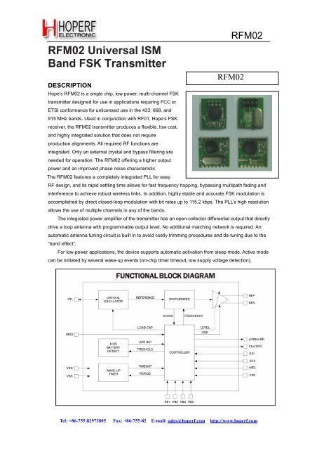
<strong>RFM02</strong> Universal ISMBand FSK TransmitterDESCRIPTIONHope’s <strong>RFM02</strong> is a single chip, low power, multi-channel FSKtransmitter designed for use in applications requiring FCC orETSI conformance for unlicensed use in the 433, 868, and915 MHz bands. Used in conjunction with RF01, Hope’s FSKreceiver, the <strong>RFM02</strong> transmitter produces a flexible, low cost,and highly integrated solution that does not requireproduction alignments. All required RF functions areintegrated. Only an external crystal and bypass filtering areneeded for operation. The <strong>RFM02</strong> offering a higher outputpower and an improved phase noise characteristic.The <strong>RFM02</strong> features a completely integrated PLL for easy<strong>RFM02</strong><strong>RFM02</strong>RF design, and its rapid settling time allows for fast frequency hopping, bypassing multipath fading andinterference <strong>to</strong> achieve robust wireless links. In addition, highly stable and accurate FSK modulation isaccomplished by direct closed-loop modulation with bit rates up <strong>to</strong> 115.2 kbps. The PLL’s high resolutionallows the use of multiple channels in any of the bands.The integrated power amplifier of the transmitter has an open-collec<strong>to</strong>r differential output that directlydrive a loop antenna with programmable output level. No additional matching network is required. Anau<strong>to</strong>matic antenna tuning circuit is built in <strong>to</strong> avoid costly trimming procedures and de-tuning due <strong>to</strong> the“hand effect”.For low-power applications, the device supports au<strong>to</strong>matic activation from sleep mode. Active modecan be initiated by several wake-up events (on-chip timer timeout, low supply voltage detection).Tel: +86-755-82973805 Fax: +86-755-82 E-mail: sales@hoperf.com http://www.hoperf.com
FEATURESFully integrated (low BOM, easy design-in)No alignment required in productionFast settling, programmable, high-resolution PLLFast frequency hopping capabilityStable and accurate FSK modulation with programmable deviationProgrammable PLL loop bandwidthDirect loop antenna driveAu<strong>to</strong>matic antenna tuning circuitProgrammable output power levelSPI bus for applications with microcontrollerClock output for microcontrollerIntegrated programmable crystal load capaci<strong>to</strong>rMultiple event handling options for wake-up activationWake-up timerLow battery detection2.2V <strong>to</strong> 5.4V supply voltageLow power consumptionLow standby current (0.3 µA)Transmit bit synchronization<strong>RFM02</strong>TYPICAL APPLICATIONS Remote control Home security and alarm Wireless keyboard/mouse and other PC peripherals Toy control Remote keyless entry Tire pressure moni<strong>to</strong>ring Telemetry Personal/patient data logging Remote au<strong>to</strong>matic meter readingDETAILED FEATURE-LEVEL DESCRIPTIONThe <strong>RFM02</strong> FSK transmitter is designed <strong>to</strong> cover the unlicensed frequency bands at 433, 868, and915 MHz. The device facilitates compliance with FCC and ETSI requirements.PLLThe programmable PLL synthesizer determines the operating frequency, while preserving accuracybased on the on-chip crystal-controlled reference oscilla<strong>to</strong>r. The PLL’s high resolution allows the usage ofmultiple channels in any of the bands. The FSK deviation is selectable (from 30 <strong>to</strong> 210 kHz with 30 kHzincrements) <strong>to</strong> accommodate various bandwidth, data rate and crystal <strong>to</strong>lerance requirements, and it isalso highly accurate due <strong>to</strong> the direct closed-loop modulation of the PLL. The transmitted digital data canbe sent asynchronously through the FSK pin or over the control interface using the appropriatecommand.RF Power Amplifier (PA)The power amplifier has an open-collec<strong>to</strong>r differential output and can directly drive a loop antennawith a programmable output power level. An au<strong>to</strong>matic antenna tuning circuit is built in <strong>to</strong> avoid costlytrimming procedures and the so-called “hand effect.”Tel: +86-755-82973805 Fax: +86-755-82 E-mail: sales@hoperf.com http://www.hoperf.com
PACKAGE PIN DEFINITIONS<strong>RFM02</strong>Pin type key: D=digital, A=analog, S=supply, I=input, O=output, IO=input/outputDefinition TYPE functionFSK DI FSK data inputCLK DO clock out for MCU (1 MHz-10 MHz)VDD S Positive power supplynIRQ DO Interrupts request output(active low)SDI DI SPI data inputSCK DI SPI clock inputVSS S negative power supply, GNDnSEL DI Chip select (active low)Typical applicationTel: +86-755-82973805 Fax: +86-755-82 E-mail: sales@hoperf.com http://www.hoperf.com
<strong>RFM02</strong>GENERAL DEVICE SPECIFICATIONAll voltages are referenced <strong>to</strong> V ss, the potential on the ground reference pin VSS.Absolute Maximum Ratings (non-operating)Symbol Parameter Min Max UnitsV dd Positive supply voltage -0.5 6.0 VV in Voltage on any pin except open collec<strong>to</strong>r outputs -0.5 V dd+0.5 VV oc Voltage on open collec<strong>to</strong>r outputs -0.5 6.0 VI in Input current in<strong>to</strong> any pin except VDD and VSS -25 25 mAESD Electrostatic discharge with human body model 1000 VT st S<strong>to</strong>rage temperature -55 125 ℃Recommended Operating RangeSymbol Parameter Min Max UnitsV dd Positive supply voltage 2.2 5.4 VV oc Voltage on open collec<strong>to</strong>r outputs (Max 6.0 V) V dd - 1 V dd + 1 VT op Ambient operating temperature -40 85 ℃ELECTRICAL SPECIFICATION(Min/max values are valid over the whole recommended operating range, typ conditions:T op =27℃;V dd =V oc=2.7V)DC CharacteristicsSymbol Parameter Conditions/Notes Min Typ Max UnitsI dd_TX_0Supply current433 MHz bandActive state with12mA(TX mode,868 MHz band0dBm14Pout =0dBm)915 MHz bandoutput power15I dd_TX_PMAX Supply current433 MHz bandActive state with21mA(TX mode,868 MHz bandmaximum output23Pout =P max)915 MHz bandpower24I pdStandby current in sleep modeAll blocks0.3 µA(Note 1)disabledI wtWake-up timer current1.5 µAconsumptionI lbLow battery detec<strong>to</strong>r currentconsumptionI x Idle current Only crystaloscilla<strong>to</strong>r is on0.5 µA1.5 mATel: +86-755-82973805 Fax: +86-755-82 E-mail: sales@hoperf.com http://www.hoperf.com
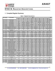
<strong>RFM02</strong>Output capacitanceAt low bands1.52.32.8C o(set by the au<strong>to</strong>maticAt high bands1.62.23.1 pFantenna tuning circuit)Q oQuality fac<strong>to</strong>r of theoutput capacitance16 18 22pFL outOutput phase noise100 kHz from carrier1 MHz from carrier (Note 7)-85-105dBc/HzBR FSK FSK bit rate (Note 7) 115.2 kbpsdf fskFSK frequencydeviationProgrammable in 30 kHz steps30 210kHzCrystal loadProgrammable in 0.5 pF steps,8.5 16C xlcapacitance SeeCrystal Selection<strong>to</strong>lerance +/-10%pFGuidelinest PORInternal POR timeout(Note 6)After V dd has reached 90% offinal value50mst sxCrystal oscilla<strong>to</strong>rstartup timeCrystal ESR < 100 Ohms1.5 5mst PBtWake-up timer clockperiodCalibrated every 30 seconds0.95 1.05mst wake-upProgrammablewake-up time1 5 *10 11msC in, Dt r, fDigital inputcapacitanceDigital output rise/falltime15 pF pure capacitive loadNote 1: Using a CR2032 battery (225 mAh capacity), the expected battery life is greater than 2 yearsusing a 60-second wake-up period for sending 50 byte packets in length at 19.2 kbps with +6 dBm outputpower in the 915 MHz band.Note 2: Using anything but a 10 MHz crystal is allowed but not recommended because allcrystal-referred timing and frequency parameters will change accordingly.Note 3: Adjustable in 8 steps.Note 4: Optimal antenna admittance/impedance for the <strong>RFM02</strong>:Yantenna [S] Zantenna [Ohm] Lantenna [nH]434 MHz 1.3E-3 - j6.3E-3 31 + j152 58.00868 MHz 1.35E-3 - j1.2E-2 9 + j82 15.20915 MHz 1.45E-3 - j1.3E-2 8.7 + j77 13.60Note 5: With selective resonant antennas .Note 6: During this period, no commands are accepted by the chip.Note 7: The maximum FSK bitrate and the Output phase noise are dependent on the actual setting of thePLL Setting Command.210pFnsTel: +86-755-82973805 Fax: +86-755-82 E-mail: sales@hoperf.com http://www.hoperf.com
<strong>RFM02</strong>TYPICAL PERFORMANCE DATA (<strong>RFM02</strong>)Phase noise measurements in the 868 MHz ISM bandUnmodulated RF SpectrumThe output spectrum is measured at different frequencies. The output is loaded with 50 Ohms through amatching network.Modulated RF SpectrumTel: +86-755-82973805 Fax: +86-755-82 E-mail: sales@hoperf.com http://www.hoperf.com
Other Important Characteristics<strong>RFM02</strong>The antenna tuning characteristics was recorded in “max-hold” state of the spectrum analyzer. During themeasurement, the transmitters were forced <strong>to</strong> change frequencies by forcing an external reference signal<strong>to</strong> the XTL pin. While the carrier was changing the antenna tuning circuit switched trough all the availablestates of the tuning circuit. The graph clearly demonstrates that while the complete output circuit hadabout a 40 MHz bandwidth, the tuning allows operating in a 220 MHz band. In other words the tuningcircuit can compensate for 25% variation in the resonant frequency due <strong>to</strong> any process or manufacturingspread.CONTROL INTERFACECommands <strong>to</strong> the transmitters are sent serially. Data bits on pin SDI are shifted in<strong>to</strong> the device upon therising edge of the clock on pin SCK whenever the chip select pin nSEL is low. When the nSEL signal ishigh, it initializes the serial interface. The number of bits sent is an integer multiple of 8. All commandsconsist of a command code, followed by a varying number of parameter or data bits. All data are sentMSB first (e.g. bit 15 for a 16-bit command). Bits having no influence (don’t care) are indicated with X.The Power On Reset (POR) circuit sets default values in all control and command registers.Timing SpecificationSymbol Parameter Minimum Value [ns]t CH Clock high time 25t CL Clock low time 25t SS Select setup time (nSEL falling edge <strong>to</strong> SCK rising edge) 10t SH Select hold time (SCK falling edge <strong>to</strong> nSEL rising edge) 10t SHI Select high time 25t DS Data setup time (SDI transition <strong>to</strong> SCK rising edge) 5t DH Data hold time (SCK rising edge <strong>to</strong> SDI transition) 5t OD Data delay time 10Tel: +86-755-82973805 Fax: +86-755-82 E-mail: sales@hoperf.com http://www.hoperf.com
Timing Diagram<strong>RFM02</strong>Control CommandsControl CommandRelated Parameters/Functions1 Configuration Setting CommandFrequency band, microcontroller clock output, crystal loadcapacitance, frequency deviation2 Power Management CommandCrystal oscilla<strong>to</strong>r, synthesizer, power amplifier, low batterydetec<strong>to</strong>r, wake-up timer, clock output buffer3 Frequency Setting Command Carrier frequency4 Data Rate Command Bit rate5 Power Setting Command Nominal output power, OOK mode6 Low Battery Detec<strong>to</strong>r Command Low battery threshold limit7 Sleep Command Length of the clock tail after power down8 Wake-Up Timer Command Wake-up time period9 Data Transmit Command Data transmission10 Status Register Command Transmitter status read11 PLL Setting Command PLL bandwidth can be modified by this commandNote: In the following tables the POR column shows the default values of the command registers afterpower-on.1. Configuration Setting Commandbit 15 14 13 12 11 10 9 8 7 6 5 4 3 2 1 0 POR1 0 0 b1 b0 d2 d1 d0 x3 x2 x1 x0 ms m2 m1 m0 8080hb1 b0 Frequency Band [MHz]0 1 4331 0 8681 1 915x3 x2 x1 x0 Crystal Load Capacitance [pF]0 0 0 0 8.50 0 0 1 9.00 0 1 0 9.51 1 16.0…………1 1 1 0 15.5Tel: +86-755-82973805 Fax: +86-755-82 E-mail: sales@hoperf.com http://www.hoperf.com
d2 d1 d0 Clock OutputFrequency [MHz]0 0 0 10 0 1 1.250 1 0 1.660 1 1 21 0 0 2.51 0 1 3.331 1 0 51 1 1 10<strong>RFM02</strong>The resulting output frequency can be calculated as:f = f0 – (-1) SIGN out* (M + 1) * (30 kHz)where:f0 is the channel center frequency (see the nextcommand)M is the three bit binary number SIGN = (ms) XOR (FSK input)Note:• Use M in a range from 0 <strong>to</strong> 6.2. Power Management Commandbit 15 14 13 12 11 10 9 8 7 6 5 4 3 2 1 0 POR1 1 0 0 0 0 0 0 a1 a0 ex es ea eb et dc C000hBits 5-0, enable the corresponding block of the transmitters, i.e. the crystal oscilla<strong>to</strong>r is enabled bythe ex bit, the synthesizer by es, the power amplifier by ea and the low battery detec<strong>to</strong>r by eb, while thewake-up timer by et. The bit dc disables the clock output buffer.When receiving the Data Transmit Command, the chip supports au<strong>to</strong>matic on/off control over thecrystal oscilla<strong>to</strong>r, the PLL and the PA.If bit a1 is set, the crystal oscilla<strong>to</strong>r and the synthesizer are controlled au<strong>to</strong>matically. Data TransmitCommand starts up the crystal oscilla<strong>to</strong>r and as soon as a stable reference frequency is available thesynthesizer starts. After a subsequent delay <strong>to</strong> allow locking of the PLL, if a0 is set the power amplifier isturned on as well.Note:To enable the au<strong>to</strong>matic internal control of the crystal oscilla<strong>to</strong>r, the synthesizer and the poweramplifier, the corresponding bits (ex, es, ea) must be zero in the Power Management Command.The ex bit should be set in the Power Management Command for the correct control of es and ea.The oscilla<strong>to</strong>r can be switched off by clearing the ex bit after the transmission.The Sleep Command can be used <strong>to</strong> indicate the end of the data transmission process.For processing the events caused by the peripheral blocks (POR, LBD or wake-up timer) the chiprequires operation of the crystal oscilla<strong>to</strong>r. This operation is fully controlled internally, independently fromthe status of the ex bit, but if the dc bit is zero, the oscilla<strong>to</strong>r remains active until Sleep Command isissued. (This command can be considered as an event controller reset.)Tel: +86-755-82973805 Fax: +86-755-82 E-mail: sales@hoperf.com http://www.hoperf.com
Oscilla<strong>to</strong>r control logic<strong>RFM02</strong>3. Frequency Setting Commandbit 15 14 13 12 11 10 9 8 7 6 5 4 3 2 1 0 POR1 0 1 0 f11 f10 f9 f8 f7 f6 f5 f4 f3 f2 f1 f0 A7D0hThe 12-bit parameter of the Frequency Setting Command has the value F. The value F shouldbe in the range of 96 and 3903. When F is out of range, the previous value is kept. The synthesizercenter frequency f 0 can be calculated as:f 0 = 10 MHz * C1 * (C2 + F/4000)The constants C1 and C2 are determined by the selected band as:Band [MHz] C1 C2433 1 43868 2 43915 3 30Note:• For correct operation of the frequency synthesizer, the frequency and band of operation need <strong>to</strong> beprogrammed before the synthesizer is started. Directly after activation of the synthesizer, the RF VCO iscalibrated <strong>to</strong> ensure proper operation in the programmed frequency band.4. Data Rate Commandbit 15 14 13 12 11 10 9 8 7 6 5 4 3 2 1 0 POR1 1 0 0 1 0 0 0 r7 r6 r5 r4 r3 r2 r1 r0 C800hThe transmitted bit rate is determined by the 8-bit value R (bits ) as:BR = 10 MHz / 29 / (R+1)Apart from setting cus<strong>to</strong>m values, the standard bit rates from 2.4 <strong>to</strong> 115.2 kbps can be approximated withminimal error.Note:• PLL bandwidth should be set according the data rate. Please see the PLL Setting Command.Tel: +86-755-82973805 Fax: +86-755-82 E-mail: sales@hoperf.com http://www.hoperf.com
<strong>RFM02</strong>after S periods of the microcontroller clock (if a1=1 and ex=0) <strong>to</strong> enable the microcontroller <strong>to</strong> execute allnecessary commands before entering sleep mode itself. The 8-bit value S is determined by bits .8. Wake-Up Timer Commandbit 15 14 13 12 11 10 9 8 7 6 5 4 3 2 1 0 POR1 1 1 r4 r3 r2 r1 r0 m7 m6 m5 m4 m3 m2 m1 m0 E000hThe wake-up time period can be calculated as:T wake-up = M * 2 R [ms],where M is defined by the digital value and R is defined by the digital value.Note:• For continual operation the et bit should be cleared and set at the end of every cycle.9. Data Transmit Commandbit 7 6 5 4 3 2 1 01 1 0 0 0 1 1 0This Command Indicates that the following bitstream coming in via the serial interface is <strong>to</strong> betransmitted.Note• This command is not needed if the transmitters’ power management bits (ex, es and ea) are fullycontrolled by the microcontroller and TX data comes through the FSK pin.• If the crystal oscilla<strong>to</strong>r was formerly switched off (ex=0), the internal oscilla<strong>to</strong>r needs t sx time, <strong>to</strong>switch on. The actual value depends on the type of quartz crystal used.• If the synthesizer was formerly switched off (es=0), the internal PLL needs t sp startup time. Valid datacan be transmitted only when the internal locking process is finished.Data Transmit Sequence Through the FSK PinTel: +86-755-82973805 Fax: +86-755-82 E-mail: sales@hoperf.com http://www.hoperf.com
Data Transmit Sequence Through the SDI Pin<strong>RFM02</strong>Note:Do not send CLK pulses with the TX data bits, otherwise they will be interpreted as commands.This mode is not SPI compatible.If the crystal oscilla<strong>to</strong>r and the PLL are running, the t sx+t sp delay is not needed.10 . Status Register Read Commandbit 15 14 13 12 11 10 9 8 7 6 5 4 3 2 1 0 POR1 1 0 0 1 1 0 0 0 0 0 0 0 0 0 0 --With this command, it is possible <strong>to</strong> read the chip’s status register through the nIRQ pin. This commandclears the last serviced interrupt and processing the next pending one will start (if there is any).Status Register Read Sequence11. PLL Setting CommandPLL bandwidth can be selected by this commandPLL command Max data rate[kbps]Phase noise at 1MHz offset[dbc/Hz]CommentsD240h 19.2 -112 25%currentD2C0h 38.4 -110 33%currentD200h 68.9 -107 50%currentD280h 115.2 -102 100%currentTel: +86-755-82973805 Fax: +86-755-82 E-mail: sales@hoperf.com http://www.hoperf.com
RX-TX ALIGNMENT PROCEDURES<strong>RFM02</strong>RX-TX frequency offset can be caused only by the differences in the actual reference frequency. Tominimize these errors it is suggested <strong>to</strong> use the same crystal type and the same PCB layout for thecrystal placement on the RX and TX PCBs.To verify the possible RX-TX offset it is suggested <strong>to</strong> measure the CLK output of both chips with ahigh level of accuracy. Do not measure the output at the XTL pin since the measurement process itselfwill change the reference frequency. Since the carrier frequencies are derived from the referencefrequency, having identical reference frequencies and nominal frequency settings at the TX and RX sidethere should be no offset if the CLK signals have identical frequencies.It is possible <strong>to</strong> moni<strong>to</strong>r the actual RX-TX offset using the AFC status report included in the statusbyte of the receiver. By reading out the status byte from the receiver the actual measured offsetfrequency will be reported. In order <strong>to</strong> get accurate values the AFC has <strong>to</strong> be disabled during the read byclearing the "en" bit in the AFC Control Command (bit 0).CRYSTAL SELECTION GUIDELINESThe crystal oscilla<strong>to</strong>r of the <strong>RFM02</strong> requires a 10 MHz parallel mode crystal. The circuit containsan integrated load capaci<strong>to</strong>r in order <strong>to</strong> minimize the external component count. The internal loadcapacitance value is programmable from 8.5 pF <strong>to</strong> 16 pF in 0.5 pF steps. With appropriate PCB layout,the <strong>to</strong>tal load capacitance value can be 10 pF <strong>to</strong> 20 pF so a variety of crystal types can be used.When the <strong>to</strong>tal load capacitance is not more than 20 pF and a worst case 7 pF shunt capacitance(C0) value is expected for the crystal, the oscilla<strong>to</strong>r is able <strong>to</strong> start up with any crystal having less than100 ohms ESR (equivalent series loss resistance). However, lower C0 and ESR values guarantee fasteroscilla<strong>to</strong>r startup. It is recommended <strong>to</strong> keep the PCB parasitic capacitances on the XTL pin as low aspossible.The crystal frequency is used as the reference of the PLL, which generates the RF carrier frequency(fc). Therefore fc is directly proportional <strong>to</strong> the crystal frequency. The accuracy requirements forproduction <strong>to</strong>lerance, temperature drift and aging can thus be determined from the maximum allowablecarrier frequency error.Tel: +86-755-82973805 Fax: +86-755-82 E-mail: sales@hoperf.com http://www.hoperf.com
Maximum XTAL Tolerances Including Temperature and Aging [ppm]<strong>RFM02</strong>Whenever a low frequency error is essential for the application, it is possible <strong>to</strong> “pull” the crystal <strong>to</strong> theaccurate frequency by changing the load capaci<strong>to</strong>r value. The widest pulling range can be achieved if thenominal required load capacitance of the crystal is in the “midrange”, for example 16 pF. The “pull-ability”of the crystal is defined by its motional capacitance and C0Note:• There may be other requirements for the TX carrier accuracy with regards <strong>to</strong> the requirements asdefined by standards and/or channel separations.EXAMPLE APPLICATIONS: DATA PACKET TRANSMISSIONData packet structureAn example data packet structure using the <strong>RFM02</strong>X - RF01 pair for data transmission. Thispacket structure is an example of how <strong>to</strong> use the high efficiency FIFO mode at the receiver side:Tel: +86-755-82973805 Fax: +86-755-82 E-mail: sales@hoperf.com http://www.hoperf.com
<strong>RFM02</strong>The first 3 bytes compose a 24 bit length ‘01’ pattern <strong>to</strong> let enough time for the clock recovery of thereceiver <strong>to</strong> lock. The next two bytes compose a 16 bit synchron pattern which is essential for thereceiver’s FIFO <strong>to</strong> find the byte synchron in the received bit stream. The synchron patters is followed bythe payload. The first byte transmitted after the synchron pattern (D0 in the picture above) will be the firstreceived byte in the FIFO.Important: The bytes of the data stream should follow each other continuously, otherwise the clockrecovery circuit of the receiver side will be unable <strong>to</strong> track.Further details of packet structures can be found in the RF ISM-UGSB1 software development kit manualTel: +86-755-82973805 Fax: +86-755-82 E-mail: sales@hoperf.com http://www.hoperf.com
REFERENCE DESIGNS<strong>RFM02</strong>SchematicPCB layoutBot<strong>to</strong>m <strong>view</strong>Tel: +86-755-82973805 Fax: +86-755-82 E-mail: sales@hoperf.com http://www.hoperf.com
<strong>RFM02</strong>Tel: +86-755-82973805 Fax: +86-755-82 E-mail: sales@hoperf.com http://www.hoperf.com
<strong>RFM02</strong>DIP PACKAGE(D)Module Definitionmodel=module-operation_band-package_type<strong>RFM02</strong>B-433-Dmodule type operation band Packageeg:1,<strong>RFM02</strong> module at 433MHz band, DIP : <strong>RFM02</strong>-433-D。2,<strong>RFM02</strong> module at 868MHz band, SMD, thickness at 4.2mm : <strong>RFM02</strong>-868-S1。Tel: +86-755-82973805 Fax: +86-755-82 E-mail: sales@hoperf.com http://www.hoperf.com
<strong>RFM02</strong><strong>HOPE</strong> MICROELECTRONICS CO.,LTDAdd:4/F, Block B3, East Industrial Area,Huaqiaocheng, Shenzhen, Guangdong,ChinaTel: 86-755-82973805Fax: 86-755-82973550Email: sales@hoperf.comWebsite: http://www.hoperf.comhttp://www.hoperf.cnhttp://hoperf.en.alibaba.comThis document may contain preliminary information and is subject <strong>to</strong>change by Hope <strong>Microelectronics</strong> without notice. Hope <strong>Microelectronics</strong>assumes no responsibility or liability for any use of the informationcontained herein. Nothing in this document shall operate as an expressor implied license or indemnity under the intellectual property rights ofHope <strong>Microelectronics</strong> or third parties. The products described in thisdocument are not intended for use in implantation or other direct lifesupport applications where malfunction may result in the direct physicalharm or injury <strong>to</strong> persons. NO WARRANTIES OF ANY KIND,INCLUDING, BUT NOT LIMITED TO, THE IMPLIED WARRANTIES OFMECHANTABILITY OR FITNESS FOR A ARTICULAR PURPOSE, AREOFFERED IN THIS DOCUMENT.©2006, <strong>HOPE</strong> MICROELECTRONICS CO.,LTD. All rights reserved.Tel: +86-755-82973805 Fax: +86-755-82 E-mail: sales@hoperf.com http://www.hoperf.com