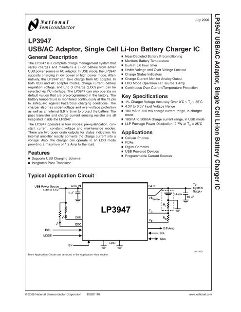
LP3947 USB/AC Adaptor, Single Cell Li-Ion Battery ... - Farnell
LP3947 USB/AC Adaptor, Single Cell Li-Ion Battery ... - Farnell
LP3947 USB/AC Adaptor, Single Cell Li-Ion Battery ... - Farnell

Create successful ePaper yourself
Turn your PDF publications into a flip-book with our unique Google optimized e-Paper software.
<strong>LP3947</strong><br />
<strong>USB</strong>/<strong>AC</strong> <strong>Adaptor</strong>, <strong>Single</strong> <strong>Cell</strong> <strong>Li</strong>-<strong>Ion</strong> <strong>Battery</strong> Charger IC<br />
General Description<br />
The <strong>LP3947</strong> is a complete charge management system that<br />
safely charges and maintains a <strong>Li</strong>-<strong>Ion</strong> battery from either<br />
<strong>USB</strong> power source or <strong>AC</strong> adaptor. In <strong>USB</strong> mode, the <strong>LP3947</strong><br />
supports charging in low power or high power mode. Alternatively,<br />
the <strong>LP3947</strong> can take charge from <strong>AC</strong> adaptor. In<br />
both <strong>USB</strong> and <strong>AC</strong> adaptor modes, charge current, battery<br />
regulation voltage, and End of Charge (EOC) point can be<br />
selected via I2C interface. The <strong>LP3947</strong> can also operate on<br />
default values that are pre-programmed in the factory. The<br />
battery temperature is monitored continuously at the Ts pin<br />
to safeguard against hazardous charging conditions. The<br />
charger also has under-voltage and over-voltage protection<br />
as well as an internal 5.6 hr timer to protect the battery. The<br />
pass transistor and charge current sensing resistor are all<br />
integrated inside the <strong>LP3947</strong>.<br />
The <strong>LP3947</strong> operates in four modes: pre-qualification, constant<br />
current, constant voltage and maintenance modes.<br />
There are two open drain outputs for status indication. An<br />
internal amplifier readily converts the charge current into a<br />
voltage. Also, the charger can operate in an LDO mode<br />
providing a maximum of 1.2 Amp to the load.<br />
Features<br />
n Supports <strong>USB</strong> Charging Scheme<br />
n Integrated Pass Transistor<br />
Typical Application Circuit<br />
More Application Circuit can be found in the Application Note section.<br />
n Near-Depleted <strong>Battery</strong> Preconditioning<br />
n Monitors <strong>Battery</strong> Temperature<br />
n Built-In 5.6 hour timer<br />
n Under Voltage and Over Voltage Lockout<br />
n Charge Status Indicators<br />
n Charge Current Monitor Analog Output<br />
n LDO Mode Operation can source 1 Amp<br />
n Continuous Over Current/Temperature Protection<br />
Key Specifications<br />
n 1% Charger Voltage Accuracy Over 0˚C ≤ T J ≤ 85˚C<br />
n 4.3V to 6.0V Input Voltage Range<br />
n 100 mA to 750 mA charge current range, in charger<br />
mode<br />
n 100mA to 500mA charge current range, in <strong>USB</strong> mode<br />
n LLP Package Power Dissipation: 2.7W at T A = 25˚C<br />
Applications<br />
n <strong>Cell</strong>ular Phones<br />
n PDAs<br />
n Digital Cameras<br />
n <strong>USB</strong> Powered Devices<br />
n Programmable Current Sources<br />
July 2006<br />
© 2006 National Semiconductor Corporation DS201110 www.national.com<br />
20111001<br />
<strong>LP3947</strong> <strong>USB</strong>/<strong>AC</strong> <strong>Adaptor</strong>, <strong>Single</strong> <strong>Cell</strong> <strong>Li</strong>-<strong>Ion</strong> <strong>Battery</strong> Charger IC
<strong>LP3947</strong><br />
Connection Diagrams and Package Mark Information<br />
Pin Descriptions<br />
(Top View)<br />
See NS Package Number SDA14B<br />
Pin # Name Description<br />
1 EN Charger Enable Input. Internally pulled high to CHG-IN pin. A HIGH enables the charger and a<br />
LOW disables the charger.<br />
2 SCL I2C serial Interface Clock input.<br />
3 SDA I2C serial Interface Data input/out.<br />
4 BATT <strong>Battery</strong> supply input terminal. Must have 10 µF ceramic capacitor to GND<br />
5 VT Regulated 2.78V output used for biasing the battery temperature monitoring thermistor.<br />
6 VBSENSE <strong>Battery</strong> Voltage Sense connected to the positive terminal of the battery.<br />
7 MODE Select pin between <strong>AC</strong> adaptor and <strong>USB</strong> port. A LOW sets the <strong>LP3947</strong> in <strong>USB</strong> port and a HIGH<br />
sets it in the <strong>AC</strong> adaptor.<br />
8 Diff-Amp Charge current monitoring differential amplifier output. Voltage output representation of the charge<br />
current.<br />
9 Ts Multi function pin. <strong>Battery</strong> temperature monitoring input and LDO/Charger mode.<br />
Pulling this pin to VT, or removing the thermistor by physically disconnecting the battery, sets the<br />
device in LDO mode.<br />
10 EOC Active Low Open Drain Output. Active when <strong>USB</strong> port or <strong>AC</strong> adaptor is connected and battery is<br />
fully charged. For more information, refer to “LED Charge Status Indicators” section.<br />
11 GND Ground<br />
12 CHG Active Low Open Drain Output. Active when <strong>USB</strong> port or <strong>AC</strong> adaptor is connected and battery is<br />
being charged. For more information, refer to “LED Charge Status Indicators” section.<br />
13 ISEL Control pin to switch between low power (100 mA) mode and high power (500 mA) mode in <strong>USB</strong><br />
mode. This pin is pulled high internally as default to set the <strong>USB</strong> in 100 mA mode. This pin has to<br />
be externally pulled low to go into 500 mA mode.<br />
14 CHG-IN Charger input from a regulated, current limited power source. Must have a1µFceramic capacitor<br />
to GND<br />
Ordering Information<br />
<strong>LP3947</strong><br />
Supplied as 1000 Units,<br />
Tape and Reel<br />
<strong>LP3947</strong><br />
Supplied as 4500 Units<br />
Tape and Reel<br />
20111002<br />
Default<br />
Options*<br />
<strong>LP3947</strong>ISD-09 <strong>LP3947</strong>ISDX-09 I CHG = 500 mA<br />
V BATT = 4.1V<br />
EOC = 0.1C<br />
<strong>LP3947</strong>ISD-51 <strong>LP3947</strong>ISDX-51 I CHG = 500 mA<br />
V BATT = 4.2V<br />
EOC = 0.1C<br />
L00061B<br />
L00062B<br />
Package<br />
Marking<br />
*Other default options are available. Please contact National Semiconductor sales office/distributors for availability and specifications.<br />
www.national.com 2
<strong>LP3947</strong> Functional Block Diagram<br />
3<br />
20111003<br />
www.national.com<br />
<strong>LP3947</strong>
<strong>LP3947</strong><br />
Absolute Maximum Ratings (Notes 1,<br />
2)<br />
If Military/Aerospace specified devices are required,<br />
please contact the National Semiconductor Sales Office/<br />
Distributors for availability and specifications.<br />
CHG-IN<br />
All pins except GND and CHG-IN<br />
−0.3V to +6.5V<br />
(Note 3) −0.3V to +6V<br />
Junction Temperature 150˚C<br />
Storage Temperature −40˚C to +150˚C<br />
Power Dissipation (Note 4)<br />
ESD (Note 5)<br />
1.89W<br />
Human Body Model<br />
2kV<br />
Machine Model<br />
200V<br />
Operating Ratings (Notes 1, 2)<br />
CHG-IN<br />
EN, ISEL, MODE, SCL, SDA,<br />
0.3V to 6.5V<br />
VT (Note 3) 0V to 6V<br />
Junction Temperature −40˚C to +125˚C<br />
Operating Temperature −40˚C to +85˚C<br />
Thermal Resistance θJA 37˚C/W<br />
Maximum Power Dissipation<br />
(Note 6)<br />
1.21W<br />
Electrical Characteristics<br />
Unless otherwise noted, VCHG-IN = 5V, VBATT = 4V, CCHG-IN = 1 µF, CBATT = 10 µF. Typical values and limits appearing in normal<br />
type apply for TJ = 25˚C. <strong>Li</strong>mits appearing in boldface type apply over the entire junction temperature range for operation,<br />
TJ = −40˚C to +85˚C. (Notes 7, 8, 9)<br />
Symbol<br />
VCC SUPPLY<br />
Parameter Conditions Typ<br />
Min<br />
<strong>Li</strong>mit<br />
Max<br />
Units<br />
VCHG-IN V<strong>USB</strong> Input Voltage Range 4.5<br />
4.3<br />
6<br />
6<br />
V<br />
ICC Quiescent Current VCHG-IN ≤ 4V 2 20<br />
EOC = Low, adaptor connected,<br />
VBATT = 4.1V<br />
50 150<br />
µA<br />
VOK-TSHD <strong>Adaptor</strong> OK Trip Point (CHG-IN) VCHG-IN –VBATT (Rising) 60 mV<br />
VCHG-IN –VBATT (Falling) 50 mV<br />
VUVLO-TSHD Under Voltage Lock-Out Trip Point VCHG-IN (Rising) 3.95 3.6 4.3 V<br />
VCHG-IN (Falling) 3.75 3.4 4.1 V<br />
VOVLO-TSHD Over Voltage Lock-Out Trip Point VCHG-IN (Rising)<br />
VCHG-IN (Falling)<br />
5.9<br />
5.7<br />
V<br />
Thermal Shutdown Temperature<br />
Thermal Shutdown Hysteresis<br />
(Note 8) 160<br />
20<br />
˚C<br />
BATTERY CHARGER<br />
ICHG Fast Charge Current Range ISEL = High, In <strong>USB</strong> Mode 100<br />
ISEL = Low, In <strong>USB</strong> Mode 500<br />
mA<br />
In <strong>AC</strong> <strong>Adaptor</strong> Mode 100 750<br />
Fast Charge Current Accuracy ICHARGE = 100 mA or 150 mA −20 +20 mA<br />
ICHARGE ≥ 200 mA −10 +10 %<br />
IPRE-CHG Pre-Charge Current VBATT =2V 45 70 mA<br />
IEOC End of Charge Current Accuracy 100 mA to 450 mA, 0.1C EOC Only<br />
(Note 10)<br />
−10 +10 mA<br />
500 mA to 750 mA, All EOC Points −20 +20 %<br />
VBATT <strong>Battery</strong> Regulation Voltage (For 4.1V TJ = 0˚C to +85˚C 4.1 4.059 4.141<br />
<strong>Cell</strong>)<br />
<strong>Battery</strong> Regulation Voltage (For 4.2V<br />
TJ = −40˚C to +85˚C<br />
TJ = 0˚C to +85˚C<br />
4.1<br />
4.1<br />
4.038<br />
4.158<br />
4.162<br />
4.242<br />
V<br />
<strong>Cell</strong>)<br />
TJ = −40˚C to +85˚C 4.2 4.137 4.263<br />
VCHG-Q Full Charge Qualification Threshold VBATT Rising, Transition from<br />
Pre-Charge to Full Current<br />
3.0 V<br />
www.national.com 4
Electrical Characteristics (Continued)<br />
Unless otherwise noted, V CHG-IN = 5V, V BATT = 4V, C CHG-IN = 1 µF, C BATT = 10 µF. Typical values and limits appearing in normal<br />
type apply for T J = 25˚C. <strong>Li</strong>mits appearing in boldface type apply over the entire junction temperature range for operation,<br />
T J = −40˚C to +85˚C. (Notes 7, 8, 9)<br />
Symbol Parameter Conditions Typ<br />
BATTERY CHARGER<br />
VBAT-RST Restart Threshold Voltage<br />
(For 4.1V <strong>Cell</strong>)<br />
Restart Threshold Voltage<br />
(For 4.2V <strong>Cell</strong>)<br />
V BATT Falling, Transition from EOC,<br />
to Pre-Qualification State<br />
V BATT Falling, Transition from EOC,<br />
to Pre-Qualification State<br />
<strong>Li</strong>mit<br />
Min Max<br />
3.9 3.77 4.02<br />
4.00 3.86 4.12<br />
RSENSE Internal Current Sense Resistance (Note 8) 120 mΩ<br />
Internal Current Sense Resistor<br />
Load Current<br />
1.2 A<br />
ICHGMON Diff-Amp Output ICHG = 50 mA 0.583<br />
ICHG = 100 mA 0.663<br />
V<br />
ICHG = 750 mA 1.790<br />
tOUT Charger Time Out TJ = 0˚C to 85˚C<br />
TJ = −40˚C to +85˚C<br />
5.625<br />
5.625<br />
4.78<br />
4.5<br />
6.42<br />
6.75<br />
Hrs<br />
VOL Low Level Output Voltage EOC, CHG Pins each at 9 mA 100 mV<br />
TEMPERATURE SENSE COMPARATORS<br />
VUTLO Low Voltage Threshold Voltage at Ts Pin, Rising<br />
Voltage at Ts Pin, Falling<br />
2.427<br />
2.369<br />
V<br />
VOTLO High Voltage Threshold Voltage at Ts Pin, Rising<br />
Voltage at Ts Pin, Falling<br />
1.470<br />
1.390<br />
V<br />
VLDO LDO Mode Voltage Threshold Voltage at Ts Pin, % of VT 97 %<br />
VT Voltage Output 2.787 V<br />
LDO MODE (Ts = HIGH)<br />
VOUT Output Voltage Regulation ILOAD = 50 mA<br />
ILOAD = 750 mA<br />
4.10<br />
4.06<br />
V<br />
LOGIC LEVELS<br />
VIL Low Level Input Voltage EN, ISEL, MODE 0.4 V<br />
VIH High Level Input Voltage EN, ISEL, MODE 2.0 V<br />
IIL Input Current EN, ISEL = LOW −10 +10 µA<br />
MODE = LOW −5 +5 µA<br />
IIH Input Current EN, ISEL, MODE = HIGH −5 +5 µA<br />
Electrical Characteristics, I 2 C Interface<br />
Unless otherwise noted, V CHG-IN =V DD = 5V, V BATT = 4V. Typical values and limits appearing in normal type apply for T J =<br />
25˚C. <strong>Li</strong>mits appearing in boldface type apply over the entire junction temperature range for operation, T J = −40˚C to +125˚C.<br />
(Notes 7, 8, 9)<br />
Symbol Parameter Conditions Typ<br />
Min<br />
<strong>Li</strong>mit<br />
Max<br />
Units<br />
VIL Low Level Input Voltage SDA & SCL (Note 8) 0.4 0.3 VDD V<br />
VIH High Level Input Voltage SDA & SCL (Note 8) 0.7 VDD VDD +0.5 V<br />
VOL Low Level Output Voltage SDA & SCL (Note 8) 0 0.2 VDD V<br />
VHYS Schmitt Trigger Input Hysteresis SDA & SCL (Note 8) 0.1 VDD V<br />
FCLK Clock Frequency (Note 8) 400 kHz<br />
tHOLD Hold Time Repeated START<br />
Condition<br />
(Note 8)<br />
0.6 µs<br />
tCLK-LP CLK Low Period (Note 8) 1.3 µs<br />
tCLK-HP CLK High Period (Note 8) 0.6 µs<br />
5<br />
Units<br />
V<br />
www.national.com<br />
<strong>LP3947</strong>
<strong>LP3947</strong><br />
Electrical Characteristics, I 2 C Interface (Continued)<br />
Unless otherwise noted, VCHG-IN =VDD = 5V, VBATT = 4V. Typical values and limits appearing in normal type apply for TJ =<br />
25˚C. <strong>Li</strong>mits appearing in boldface type apply over the entire junction temperature range for operation, TJ = −40˚C to +125˚C.<br />
(Notes 7, 8, 9)<br />
Symbol Parameter Conditions Typ<br />
Min<br />
<strong>Li</strong>mit<br />
Max<br />
Units<br />
tSU Set-Up Time Repeated START<br />
Condition<br />
(Note 8)<br />
0.6 µs<br />
tDATA-HOLD Data Hold Time (Note 8) 300 ns<br />
tDATA-SU Data Set-Up Time (Note 8) 100 ns<br />
tSU Set-Up Time for STOP Condition (Note 8) 0.6 µs<br />
tTRANS Maximum Pulse Width of Spikes that (Note 8)<br />
must be Suppressed by the Input<br />
Filter of both DATA & CLK Signals.<br />
50 ns<br />
Note 1: Absolute Maximum Ratings are limits beyond which damage to the device may occur. Operating Ratings are conditions under which operation of the device<br />
is guaranteed. Operating Ratings do not imply guaranteed performance limits. For guaranteed performance limits and associated test conditions, see the Electrical<br />
Characteristics tables.<br />
Note 2: All voltages are with respect to the potential at the GND pin.<br />
Note 3: Caution must be taken to avoid raising pins EN and VT 0.3V higher than VCHG-IN and raising pins ISEL, MODE, SCL and SDA 0.3V higher than VBATT. Note 4: The Absolute Maximum power dissipation depends on the ambient temperature and can be calculated using the formula<br />
P=(T J –T A)θ JA, (1)<br />
where TJ is the junction temperature, TA is the ambient temperature, and θJA is the junction-to-ambient thermal resistance. The 1.89W rating appearing under<br />
Absolute Maximum Ratings results from substituting the Absolute Maximum junction temperature, 150˚C, for TJ, 80˚C for TA, and 37˚C/W for θJA. More power can<br />
be dissipated safely at ambient temperatures below 80˚C. Less power can be dissipated safely at ambient temperatures above 80˚C. The Absolute Maximum power<br />
dissipation can be increased by 27 mW for each degree below 80˚C, and it must be de-rated by 27 mW for each degree above 80˚C.<br />
Note 5: The human-body model is used. The human-body model is 100 pF discharged through 1.5 kΩ.<br />
Note 6: <strong>Li</strong>ke the Absolute Maximum power dissipation, the maximum power dissipation for operation depends on the ambient temperature. The 1.21W rating<br />
appearing under Operating Ratings results from substituting the maximum junction temperature for operation, 125˚C, for TJ, 80˚C for TA, and 37˚C/W for θJA into<br />
(1) above. More power can be dissipated at ambient temperatures below 80˚C. Less power can be dissipated at ambient temperatures above 80˚C. The maximum<br />
power dissipation for operation can be increased by 27 mW for each degree below 80˚C, and it must be de-rated by 27 mW for each degree above 80˚C.<br />
Note 7: All limits are guaranteed. All electrical characteristics having room-temperature limits are tested during production with TJ = 25˚C. All hot and cold limits are<br />
guaranteed by correlating the electrical characteristics to process and temperature variations and applying statistical process control.<br />
Note 8: Guaranteed by design.<br />
Note 9: <strong>LP3947</strong> is not intended as a <strong>Li</strong>-<strong>Ion</strong> battery protection device, any battery used in this application should have an adequate internal protection.<br />
Note 10: The ±10 mA limits apply to all charge currents from 100 mA to 450 mA, to 0.1C End Of Charge (EOC). The limits increase proportionally with higher EOC<br />
points. For example, at 0.2C, the End Of Charge current accuracy becomes ±20 mA.<br />
FIGURE 1. <strong>Li</strong>-<strong>Ion</strong> Charging Profile<br />
www.national.com 6<br />
20111004
Application Notes<br />
<strong>LP3947</strong> CHARGER OPERATION<br />
The <strong>LP3947</strong> charge cycle is initiated with <strong>AC</strong> adaptor or <strong>USB</strong><br />
power source insertion. If the voltage on the CHG-IN pin<br />
meets under-voltage (VUVLO-TSHD), over-voltage (VOVLO- TSHD) requirements, and the <strong>Adaptor</strong> OK signal is detected,<br />
then pre-qualification cycle begins (see Figure 1). In this<br />
cycle, a safe current level, less than 70mA, is pumped into<br />
the battery while the voltage across the battery terminals is<br />
measured. Once this voltage exceeds 3.0V, the controller<br />
will initiate constant current fast charge cycle. If the CHG-IN<br />
pin is connected to an <strong>AC</strong> adaptor, the default charge current<br />
is 500 mA and I2C interface can be used to program this<br />
parameter. If the CHG-IN pin is connected to the <strong>USB</strong> port,<br />
constant current cycle will start with a default of 100 mA.<br />
During this cycle, the 5.6 hr safety timer starts counting.<br />
If the 5.6 hr safety timers times out during constant current<br />
cycle, charging is terminated. As the battery is charged<br />
during constant current mode, the voltage across pack terminal<br />
increases until it reaches 4.2V (or 4.1V). As soon as<br />
pack terminal reaches 4.2V (or 4.1V), the controller starts<br />
operating in constant voltage mode by applying regulated<br />
FIGURE 2. <strong>LP3947</strong> with External Switch<br />
7<br />
VBATT voltage across the battery terminals. During this cycle,<br />
the charge current, ICHG, continues to decrease with time<br />
and when it drops below 0.1C (default value), the EOC<br />
signal is activated indicating successful completion of the<br />
charge cycle. The EOC current can be programmed to 0.1C,<br />
0.15C, or 0.2C. The default value is 0.1C. After completing<br />
the full charge cycle, the controller will start the maintenance<br />
cycle where battery pack voltage is monitored continuously.<br />
During the maintenance cycle, if the pack voltage drops 200<br />
mV below the termination voltage, charge cycle will be initiated<br />
providing that the wall adaptor is plugged in and is alive.<br />
Charging terminates when the battery temperature is out of<br />
range. For more explanation, please refer to “Ts Pin” section.<br />
The <strong>LP3947</strong> with I2C interface allows maximum flexibility in<br />
selecting the charge current, battery regulation voltage and<br />
EOC current. The <strong>LP3947</strong> operates in default mode during<br />
power up. See the “I2C Interface” section for more detail.<br />
When charging source comes from the <strong>USB</strong> port, charging<br />
starts with 100 mA (low power mode, ISEL = high). The <strong>USB</strong><br />
controller can set the ISEL pin low to charge the battery at<br />
500 mA. A simple external circuit selects between an <strong>AC</strong><br />
adaptor or the <strong>USB</strong> port. The circuit is designed with priority<br />
given to the <strong>AC</strong> adaptor.<br />
20111006<br />
www.national.com<br />
<strong>LP3947</strong>
<strong>LP3947</strong><br />
Application Notes (Continued)<br />
FIGURE 3. <strong>LP3947</strong> Charger Flow Chart<br />
www.national.com 8<br />
20111007
Application Notes (Continued)<br />
CHARGE CURRENT SELECTION IN CONSTANT<br />
CURRENT MODE<br />
In the <strong>AC</strong> adaptor mode, the <strong>LP3947</strong> is designed to provide<br />
a charge current ranging from 100 mA to 750 mA, in steps of<br />
50 mA, to support batteries with different capacity ratings.<br />
The default value is 500 mA. No external resistor is required<br />
TABLE 1. Charge Current Selection in <strong>AC</strong> <strong>Adaptor</strong>/<strong>USB</strong> Mode<br />
to set the charge current in the <strong>LP3947</strong>. In the <strong>USB</strong> mode,<br />
the <strong>LP3947</strong> will initially charge with 100 mA (ISEL = high). By<br />
setting the ISEL pin low, charge current can be programmed<br />
to 500 mA. In addition, with ISEL = low, the charge current<br />
can be programmed to different values via the I 2 C interface.<br />
MODE Pin ISEL Pin Functions<br />
<strong>AC</strong> <strong>Adaptor</strong> Mode HIGH HIGH ISEL polarity is irrelevant. Default 500 mA charge current. Can be<br />
reprogrammed via I2 HIGH LOW<br />
C.<br />
<strong>USB</strong> Mode LOW HIGH 100 mA charge current<br />
LOW LOW Default 500 mA charge current. Can be reprogrammed via I2C. BATTERY VOLTAGE SELECTION<br />
The battery voltage regulation can be set to 4.1V or 4.2V by<br />
default. Please refer to the Ordering Information table for<br />
more detail.<br />
END OF CHARGE (EOC) CURRENT SELECTION<br />
The EOC thresholds can be programmed to 0.1C, 0.15C or<br />
0.2C in the <strong>LP3947</strong>. The default value is 0.1C, which provides<br />
the highest energy storage, but at the expense of<br />
longer charging time. On the other hand, 0.2C takes the<br />
least amount of charging time, but yields the least energy<br />
storage.<br />
Monitoring the Diff Amp output during constant voltage cycle<br />
can provide an accurate indication of the battery charge<br />
status and time remaining to EOC. This feature is particularly<br />
useful during constant voltage mode. The current sense<br />
circuit is operational in the LDO mode as well. It can be used<br />
to monitor the system current consumption during testing.<br />
FIGURE 4. Charge Current Monitoring Circuit (Diff-Amp)<br />
9<br />
CHARGE CURRENT SENSE DIFFERENTIAL AMPLIFIER<br />
The charge current is monitored across the internal 120 mΩ<br />
current sense resistor. The differential amplifier provides the<br />
analog representation of the charge current. Charge current<br />
can be calculated using the following equation:<br />
Where voltage at Diff Amp output (V DIFF) is in volt, and<br />
charge current (I CHG) is in amps.<br />
20111009<br />
LED CHARGE STATUS INDICATORS<br />
The <strong>LP3947</strong> is equipped with two open drain outputs to drive<br />
a green LED and a red LED. These two LEDs work together<br />
in combinations to indicate charge status or fault conditions.<br />
Table 2 shows all the conditions.<br />
www.national.com<br />
<strong>LP3947</strong>
<strong>LP3947</strong><br />
Application Notes (Continued)<br />
TABLE 2. LED Indicator Summary<br />
RED LED GREEN LED<br />
(CHG)<br />
(EOC)<br />
Charger Off OFF OFF<br />
Charging <strong>Li</strong> <strong>Ion</strong> <strong>Battery</strong>* ON OFF<br />
Maintenance Mode OFF ON<br />
Charging <strong>Li</strong> <strong>Ion</strong> <strong>Battery</strong> after Passing Maintenance Mode OFF ON<br />
EN Pin = LOW OFF ON<br />
LDO Mode OFF OFF<br />
5.6 Hr Safety Timer Flag/<strong>Battery</strong> Temperature Violation<br />
* Charging <strong>Li</strong> <strong>Ion</strong> battery for the first time after VCHG-IN insertion.<br />
ON ON<br />
Ts PIN<br />
The <strong>LP3947</strong> continuously monitors the battery temperature<br />
by measuring the voltage between the Ts pin and ground.<br />
Charging stops if the battery temperature is outside the<br />
permitted temperature range set by the battery’s internal<br />
thermistor RT and the external bias resistor RS. A 1% precision<br />
resistor should be used for RS. A curve 2 type thermistor<br />
is recommended for RT. The voltage across RT is proportional<br />
to the battery temperature. If the battery temperature is<br />
outside of the range during the charge cycle, the <strong>LP3947</strong> will<br />
suspend charging. As an example, for a temperature range<br />
of 0˚C to 50˚C, a 10kΩ for the thermistor and a 4.1kΩ for Rs should be used. When battery temperature returns to the<br />
permitted range, charging resumes from the beginning of the<br />
flow chart and the 5.6 hr safety timer is reset. Refer to Figure<br />
3. <strong>LP3947</strong> Charger Flow Chart for more information.<br />
In absence of the thermistor, Ts pin will be pulled high to VT<br />
and the <strong>LP3947</strong> goes into LDO mode. In this mode, the<br />
internal power FET provides up to 1.2 amp of current at the<br />
BATT pin. The LDO output is set to 4.1V or 4.2V, depending<br />
on the programmed battery regulation voltage. When operating<br />
at higher output currents, care must be taken not to<br />
exceed the package power dissipation rating. See “Thermal<br />
Performance of LLP Package” section for more detail.<br />
Charger Status in Relation to Ts Voltage<br />
Voltage on the Ts Pin Charger Status<br />
Ts ≥ 2.7V LDO Mode<br />
www.national.com 10<br />
Voltage on the Ts Pin Charger Status<br />
2.427v ≤ Ts < 2.7V<br />
0V ≤ Ts ≤ 1.39V<br />
Charger Off<br />
1.39V < Ts < 2.427V Charger On<br />
LDO MODE<br />
The charger is in the LDO mode when the Ts pin is left<br />
floating. This mode of operation is used primarily during<br />
system level testing of the handset to eliminate the need for<br />
battery insertion. CAUTION: battery may be damaged if<br />
device is operating in LDO mode with battery connected.<br />
The internal power FET provides up to 1.2 amp of current at<br />
BATT pin in this mode. The LDO output is set to 4.1V. When<br />
operating at higher output currents, care must be taken not<br />
to exceed the package power dissipation rating. See “Thermal<br />
Performance of LLP Package” section for more detail.<br />
EN PIN<br />
The Enable pin is used to enable/disable the charger, in both<br />
the charger mode and the LDO mode, see Figures 5, 6. The<br />
enable pin is internally pulled HIGH to the CHG-IN pin. When<br />
the charger is disabled, it draws less than 4 µA of current.
Application Notes (Continued)<br />
FIGURE 5. Power Up Timing Diagram in Charger Mode (1.39V < Ts < 2.427V)<br />
MODE PIN<br />
The mode pin toggles the <strong>LP3947</strong> between the <strong>AC</strong> adaptor<br />
mode and the <strong>USB</strong> mode. When CHG-IN is connected to a<br />
<strong>USB</strong> port, this pin must be set low. When CHG-IN is connected<br />
to an <strong>AC</strong> adaptor, this pin must be tied high to either<br />
the BATT pin or to the wall adaptor input. Caution: MODE pin<br />
should never be tied to CHG-IN pin directly, as it will turn on<br />
an internal diode.<br />
5.6 HR SAFETY TIMER IN CHARGER MODE<br />
The <strong>LP3947</strong> has a built-in 5.6 hr back up safety timer to<br />
prevent over-charging a <strong>Li</strong> <strong>Ion</strong> battery. The 5.6 hr timer starts<br />
counting when the charger enters the constant current<br />
FIGURE 6. Power Up Timing Diagram in LDO Mode (Ts ≥ 2.7V)<br />
11<br />
20111011<br />
20111010<br />
mode. It will turn the charger off when the 5.6 hr timer is up<br />
while the charger is still in constant current mode. In this<br />
case, both LEDs will turn on, indicating a fault condition.<br />
When the battery temperature is outside the specified temperature<br />
range, the 5.6 hr safety timer will reset upon recovery<br />
of the battery temperature.<br />
I2C INTERF<strong>AC</strong>E<br />
I2C interface is used in the <strong>LP3947</strong> to program various<br />
parameters as shown in Table 3. The <strong>LP3947</strong> operates on<br />
default settings following power up. Once programmed, the<br />
<strong>LP3947</strong> retains the register data as long as the battery<br />
voltage is above 2.85V.<br />
www.national.com<br />
<strong>LP3947</strong>
<strong>LP3947</strong><br />
Application Notes (Continued)<br />
TABLE 3. <strong>LP3947</strong> Serial Port Communication address code 7h’47<br />
<strong>LP3947</strong> Control and Data Codes<br />
Addrs Register 7 6 5 4 3 2 1 0<br />
8'h00 Charger<br />
Batt Voltage <strong>AC</strong> <strong>Adaptor</strong> <strong>AC</strong> <strong>Adaptor</strong> <strong>AC</strong> <strong>Adaptor</strong> <strong>AC</strong> <strong>Adaptor</strong><br />
Register -1<br />
(0) = 4.1V Charge Charge Charge Charge<br />
1 = 4.2V Current Current Current Current<br />
Code 3 Code 2 Code 1 Code 0<br />
(1)<br />
(0)<br />
(0)<br />
(0)<br />
8'h01 Charger<br />
EOC Charging EOC<br />
EOC<br />
Register -2<br />
(Green LED) (Red LED) SEL-1 SEL-0<br />
R/O<br />
R/O<br />
(0)<br />
(1)<br />
8'h02 Charger<br />
<strong>USB</strong><br />
<strong>USB</strong><br />
<strong>USB</strong><br />
<strong>USB</strong><br />
Register -3<br />
Charge Charge Charge Charge<br />
Current Current Current Current<br />
Code 3 Code 2 Code 1 Code 0<br />
(1)<br />
(0)<br />
(0)<br />
(0)<br />
Numbers in parentheses indicate default setting. “0” bit is set to low state, and “1” bit is set to high state. R/O –Read Only, All other bits are Read and Write.<br />
w = write (sda = “0”)<br />
r = read (sda = “1”)<br />
ack = acknowledge (sda pulled low by either master or slave)<br />
Nack = No Acknowledge<br />
rs = repeated start<br />
TABLE 4. Charger Current and EOC Current Programming Code<br />
Data Code<br />
Charger Current<br />
Selection Code ISET (mA)<br />
4h'00 100<br />
End of Charge Current<br />
Selection Code<br />
4h'01 150 0.1C<br />
4h'02 200 0.15C<br />
4h'03 250 0.2C<br />
4h'04 300<br />
4h'05 350<br />
4h'06 400<br />
4h'07 450<br />
4h'08 500<br />
4h'09 550<br />
4h'0A 600<br />
4h'0B 650<br />
4h'0C 700<br />
4h'0D 750<br />
FIGURE 7. <strong>LP3947</strong> (Slave) Register Write<br />
www.national.com 12<br />
20111012
Application Notes (Continued)<br />
w = write (sda = “0”)<br />
r = read (sda = “1”)<br />
ack = acknowledge (sda pulled low by either master or slave)<br />
Nack = No Acknowledge<br />
rs = repeated start<br />
THERMAL PERFORMANCE OF LLP P<strong>AC</strong>KAGE<br />
The <strong>LP3947</strong> is a monolithic device with an integrated pass<br />
transistor. To enhance the power dissipation performance,<br />
the Leadless Lead frame Package, or LLP, is used. The LLP<br />
package is designed for improved thermal performance because<br />
of the exposed die attach pad at the bottom center of<br />
the package. It brings advantage to thermal performance by<br />
creating a very direct path for thermal dissipation. Compared<br />
to the traditional leaded packages where the die attach pad<br />
is embedded inside the mold compound, the LLP reduces a<br />
layer of thermal path.<br />
The thermal advantage of the LLP package is fully realized<br />
only when the exposed die attach pad is soldered down to a<br />
thermal land on the PCB board and thermal vias are planted<br />
underneath the thermal land. Based on a LLP thermal measurement,<br />
junction to ambient thermal resistance (θJA) can<br />
be improved by as much as two times if a LLP is soldered on<br />
the board with thermal land and thermal vias than if not.<br />
An example of how to calculate for LLP thermal performance<br />
is shown below:<br />
By substituting 37˚C/W for θ JA, 125˚C for T J and 70˚C for T A,<br />
the maximum power dissipation allowed from the chip is<br />
1.48W. If V CHG-IN is at 5.0V and a 3.0V battery is being<br />
FIGURE 8. <strong>LP3947</strong> (Slave) Register Read<br />
13<br />
20111013<br />
charged, then 740 mA of I CHG can safely charge the battery.<br />
More power can be dissipated at ambient temperatures<br />
below 70˚C. Less power can be dissipated at ambient temperatures<br />
above 70˚C. The maximum power dissipation for<br />
operation can be increased by 27 mW for each degree below<br />
70˚C, and it must be de-rated by 27 mW for each degree<br />
above 70˚C.<br />
LAYOUT CONSIDERATION<br />
The <strong>LP3947</strong> has an exposed die attach pad located at the<br />
bottom center of the LLP package. It is imperative to create<br />
a thermal land on the PCB board when designing a PCB<br />
layout for the LLP package. The thermal land helps to conduct<br />
heat away from the die, and the land should be the<br />
same dimension as the exposed pad on the bottom of the<br />
LLP (1:1 ratio). In addition, thermal vias should be added<br />
inside the thermal land to conduct more heat away from the<br />
surface of the PCB to the ground plane. Typical pitch and<br />
outer diameter for these thermal vias are 1.27 mm and 0.33<br />
mm respectively. Typical copper via barrel plating is 1oz<br />
although thicker copper may be used to improve thermal<br />
performance. The <strong>LP3947</strong> bottom pad is connected to<br />
ground. Therefore, the thermal land and vias on the PCB<br />
board need to be connected to ground.<br />
For more information on board layout techniques, refer to<br />
Application Note 1187 “Leadless Leadframe Package<br />
(LLP).” The application note also discusses package handling,<br />
solder stencil, and assembly.<br />
www.national.com<br />
<strong>LP3947</strong>
<strong>LP3947</strong> <strong>USB</strong>/<strong>AC</strong> <strong>Adaptor</strong>, <strong>Single</strong> <strong>Cell</strong> <strong>Li</strong>-<strong>Ion</strong> <strong>Battery</strong> Charger IC<br />
Physical Dimensions inches (millimeters) unless otherwise noted<br />
NS Package Number SDA14B<br />
National does not assume any responsibility for use of any circuitry described, no circuit patent licenses are implied and National reserves<br />
the right at any time without notice to change said circuitry and specifications.<br />
For the most current product information visit us at www.national.com.<br />
LIFE SUPPORT POLICY<br />
NATIONAL’S PRODUCTS ARE NOT AUTHORIZED FOR USE AS CRITICAL COMPONENTS IN LIFE SUPPORT DEVICES OR SYSTEMS<br />
WITHOUT THE EXPRESS WRITTEN APPROVAL OF THE PRESIDENT AND GENERAL COUNSEL OF NATIONAL SEMICONDUCTOR<br />
CORPORATION. As used herein:<br />
1. <strong>Li</strong>fe support devices or systems are devices or systems<br />
which, (a) are intended for surgical implant into the body, or<br />
(b) support or sustain life, and whose failure to perform when<br />
properly used in accordance with instructions for use<br />
provided in the labeling, can be reasonably expected to result<br />
in a significant injury to the user.<br />
2. A critical component is any component of a life support<br />
device or system whose failure to perform can be reasonably<br />
expected to cause the failure of the life support device or<br />
system, or to affect its safety or effectiveness.<br />
BANNED SUBSTANCE COMPLIANCE<br />
National Semiconductor follows the provisions of the Product Stewardship Guide for Customers (CSP-9-111C2) and Banned Substances<br />
and Materials of Interest Specification (CSP-9-111S2) for regulatory environmental compliance. Details may be found at:<br />
www.national.com/quality/green.<br />
Lead free products are RoHS compliant.<br />
National Semiconductor<br />
Americas Customer<br />
Support Center<br />
Email: new.feedback@nsc.com<br />
Tel: 1-800-272-9959<br />
www.national.com<br />
National Semiconductor<br />
Europe Customer Support Center<br />
Fax: +49 (0) 180-530 85 86<br />
Email: europe.support@nsc.com<br />
Deutsch Tel: +49 (0) 69 9508 6208<br />
English Tel: +44 (0) 870 24 0 2171<br />
Français Tel: +33 (0) 1 41 91 8790<br />
National Semiconductor<br />
Asia Pacific Customer<br />
Support Center<br />
Email: ap.support@nsc.com<br />
National Semiconductor<br />
Japan Customer Support Center<br />
Fax: 81-3-5639-7507<br />
Email: jpn.feedback@nsc.com<br />
Tel: 81-3-5639-7560