Low Noise Figure of Cascaded LNA at 5.8 GHz Using T ... - ijimt
Low Noise Figure of Cascaded LNA at 5.8 GHz Using T ... - ijimt
Low Noise Figure of Cascaded LNA at 5.8 GHz Using T ... - ijimt

Create successful ePaper yourself
Turn your PDF publications into a flip-book with our unique Google optimized e-Paper software.
Intern<strong>at</strong>ional Journal <strong>of</strong> Innov<strong>at</strong>ion, Management and Technology, Vol. 3, No. 6, December 2012<br />
temper<strong>at</strong>ure), and B is the bandwidth (MHz). Then,<br />
equ<strong>at</strong>ion (2.4) becomes<br />
(2.7)<br />
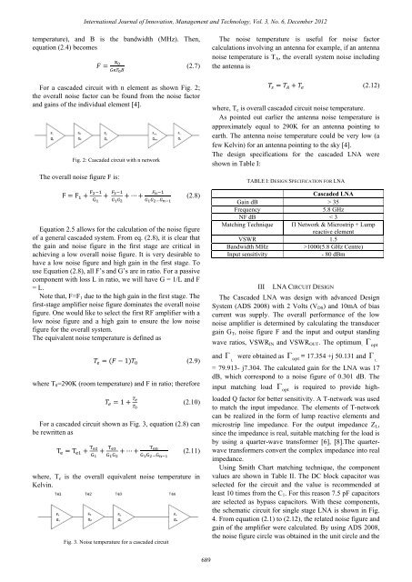
For a cascaded circuit with n element as shown Fig. 2;<br />
the overall noise factor can be found from the noise factor<br />
and gains <strong>of</strong> the individual element [4].<br />
Fig. 2: <strong>Cascaded</strong> circuit with n network<br />
The overall noise figure F is:<br />
(2.8)<br />
Equ<strong>at</strong>ion 2.5 allows for the calcul<strong>at</strong>ion <strong>of</strong> the noise figure<br />
<strong>of</strong> a general cascaded system. From eq. (2.8), it is clear th<strong>at</strong><br />
the gain and noise figure in the first stage are critical in<br />
achieving a low overall noise figure. It is very desirable to<br />
have a low noise figure and high gain in the first stage. To<br />
use Equ<strong>at</strong>ion (2.8), all F’s and G’s are in r<strong>at</strong>io. For a passive<br />
component with loss L in r<strong>at</strong>io, we will have G = 1/L and F<br />
= L.<br />
Note th<strong>at</strong>, F=F 1 due to the high gain in the first stage. The<br />
first-stage amplifier noise figure domin<strong>at</strong>es the overall noise<br />
figure. One would like to select the first RF amplifier with a<br />
low noise figure and a high gain to ensure the low noise<br />
figure for the overall system.<br />
The equivalent noise temper<strong>at</strong>ure is defined as<br />
(2.9)<br />
where T 0 =290K (room temper<strong>at</strong>ure) and F in r<strong>at</strong>io; therefore<br />
(2.10)<br />
For a cascaded circuit shown as Fig. 3, equ<strong>at</strong>ion (2.8) can<br />
be rewritten as<br />
(2.11)<br />
where, T e is the overall equivalent noise temper<strong>at</strong>ure in<br />
Kelvin.<br />
Fig. 3. <strong>Noise</strong> temper<strong>at</strong>ure for a cascaded circuit<br />
The noise temper<strong>at</strong>ure is useful for noise factor<br />
calcul<strong>at</strong>ions involving an antenna for example, if an antenna<br />
noise temper<strong>at</strong>ure is T A , the overall system noise including<br />
the antenna is<br />
(2.12)<br />
where, T e is overall cascaded circuit noise temper<strong>at</strong>ure.<br />
As pointed out earlier the antenna noise temper<strong>at</strong>ure is<br />
approxim<strong>at</strong>ely equal to 290K for an antenna pointing to<br />
earth. The antenna noise temper<strong>at</strong>ure could be very low (a<br />
few Kelvin) for an antenna pointing to the sky [4].<br />
The design specific<strong>at</strong>ions for the cascaded <strong>LNA</strong> were<br />
shown in Table I:<br />
TABLE I: DESIGN SPECIFICATION FOR <strong>LNA</strong><br />
III<br />
<strong>LNA</strong> CIRCUIT DESIGN<br />
The <strong>Cascaded</strong> <strong>LNA</strong> was design with advanced Design<br />
System (ADS 2008) with 2 Volts (V DS ) and 10mA <strong>of</strong> bias<br />
current was supply. The overall performance <strong>of</strong> the low<br />
noise amplifier is determined by calcul<strong>at</strong>ing the transducer<br />
gain G T , noise figure F and the input and output standing<br />
wave r<strong>at</strong>ios, VSWR IN and VSWR OUT . The optimum , Γ<br />
and<br />
<strong>Cascaded</strong> <strong>LNA</strong><br />
Gain dB > 35<br />
Frequency<br />
<strong>5.8</strong> <strong>GHz</strong><br />
NF dB < 3<br />
M<strong>at</strong>ching Technique Π Network & Microstrip + Lump<br />
reactive element<br />
VSWR 1.5<br />
Bandwidth MHz<br />
>1000(<strong>5.8</strong> <strong>GHz</strong> Centre)<br />
Input sensitivity<br />
- 80 dBm<br />
Γ were obtained as<br />
L<br />
Γ<br />
opt<br />
= 17.354 +j 50.131 and<br />
opt<br />
= 79.913- j7.304. The calcul<strong>at</strong>ed gain for the <strong>LNA</strong> was 17<br />
dB, which correspond to a noise figure <strong>of</strong> 0.301 dB. The<br />
input m<strong>at</strong>ching load Γ is required to provide highloaded<br />
Q factor for better sensitivity. A T-network was used<br />
to m<strong>at</strong>ch the input impedance. The elements <strong>of</strong> T-network<br />
can be realized in the form <strong>of</strong> lump reactive elements and<br />
microstrip line impedance. For the output impedance Z L ,<br />
since the impedance is real, suitable m<strong>at</strong>ching for the load is<br />
by using a quarter-wave transformer [6], [8].The quarterwave<br />
transformers convert the complex impedance into real<br />
impedance.<br />
<strong>Using</strong> Smith Chart m<strong>at</strong>ching technique, the component<br />
values are shown in Table II. The DC block capacitor was<br />
selected for the circuit and the value is recommended <strong>at</strong><br />
least 10 times from the C 1 . For this reason 7.5 pF capacitors<br />
are selected as bypass capacitors. With these components,<br />
the schem<strong>at</strong>ic circuit for single stage <strong>LNA</strong> is shown in Fig.<br />
4. From equ<strong>at</strong>ion (2.1) to (2.12), the rel<strong>at</strong>ed noise figure and<br />
gain <strong>of</strong> the amplifier were calcul<strong>at</strong>ed. By using ADS 2008,<br />
the noise figure circle was obtained in the unit circle and the<br />
opt<br />
Γ<br />
L<br />
689