Comparative Study of Microstrip Patch Antenna for Wireless - IJIMT
Comparative Study of Microstrip Patch Antenna for Wireless - IJIMT
Comparative Study of Microstrip Patch Antenna for Wireless - IJIMT

You also want an ePaper? Increase the reach of your titles
YUMPU automatically turns print PDFs into web optimized ePapers that Google loves.
International Journal <strong>of</strong> Innovation, Management and Technology, Vol. 1, No. 2, June 2010<br />
ISSN: 2010-0248<br />
<strong>Comparative</strong> <strong>Study</strong> <strong>of</strong> <strong>Microstrip</strong> <strong>Patch</strong> <strong>Antenna</strong><br />
<strong>for</strong> <strong>Wireless</strong> Communication Application<br />
Jagdish. M. Rathod, Member, IACSIT, IETE (I), IE (I), BES (I)<br />
Abstract — This paper describes variety <strong>of</strong> feeding technique<br />
applicable to microstrip patch antenna which is one <strong>of</strong> the<br />
important aspects. A good impedance matching condition<br />
between the line and patch without any additional matching<br />
elements depends heavily on feeding techniques used. After<br />
describing various feeding techniques, the paper gives a better<br />
understanding <strong>of</strong> the design parameters <strong>of</strong> an antenna and their<br />
effect on bandwidth and gain. Finally, simulation is done using<br />
design s<strong>of</strong>tware IE3D. The Coaxial Probe Feed <strong>Microstrip</strong><br />
antenna provides a bandwidth <strong>of</strong> around 20%. For aperture<br />
coupled antenna the simulated results <strong>of</strong> IE3D agrees well with<br />
the results generated by ANN (Artificial Neural Network<br />
model).<br />
Index Terms – <strong>Microstrip</strong> <strong>Patch</strong> <strong>Antenna</strong>s, Gain, Bandwidth,<br />
IE3D, Feeding Techniques, Artificial Neural Network.<br />
I. INTRODUCTION<br />
<strong>Microstrip</strong> patch antennas have various advantages such as<br />
low pr<strong>of</strong>ile, light weight, easy fabrication and con<strong>for</strong>mability<br />
to mounting hosts in addition size reduction and bandwidth<br />
enhancement are major design considerations <strong>for</strong> practical<br />
applications <strong>of</strong> microstrip antennas. Numbers <strong>of</strong> numerical<br />
methods have been developed by various researchers to ease<br />
computational ef<strong>for</strong>ts when designing microstrip patch<br />
antennas [1] which includes MoM based method. MoM<br />
involves the use <strong>of</strong> the Sommerfeld-type integrals to solve the<br />
dielectric slab Green's function. A comparison between<br />
various feeding techniques has been done. Finally, a<br />
microstrip patch antenna at specific frequency i.e. 1.25 GHz<br />
has been designed and, simulated on the design s<strong>of</strong>tware<br />
IE3D <strong>for</strong> a better understanding <strong>of</strong> the design parameters <strong>of</strong><br />
an antenna and their effect on the bandwidth and gain<br />
patterns. Input data have been generated from IE3D<br />
simulation s<strong>of</strong>tware <strong>for</strong> the ANN model.<br />
Input data consists <strong>of</strong> variation <strong>of</strong> the antenna reflection<br />
coefficient S(1, 1) and antenna impedance Z (1, 1) with<br />
various antenna parameters such as length and width <strong>of</strong> the<br />
patch, height <strong>of</strong> dielectric, patch <strong>of</strong>fsets in X and Y direction,<br />
probe radius, slot length, stub length, probe centre, patch<br />
centre etc <strong>for</strong> S-band aperture coupled microstrip antenna and<br />
an L-band capacitively coupled microstrip antenna. The data<br />
set was used to train and validate the ANN model.<br />
II. TYPES OF FEED<br />
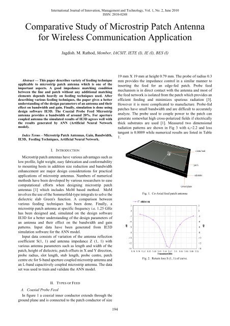
A. Coaxial Probe Feed<br />
In figure 1 a coaxial inner conductor extends through the<br />
ground plane and is connected to the patch conductor <strong>of</strong> size<br />
194<br />
19 mm X 19 mm at height 0.79 mm. The probe <strong>of</strong> radius 0.3<br />
mm provides the impedance control in a similar manner to<br />
inserting the feed <strong>for</strong> an edge-fed patch. Probe feed<br />
mechanism is in direct contact with the antenna and most <strong>of</strong><br />
the feed network is isolated from the patch which provides an<br />
efficient feeding and minimizes spurious radiation [3].<br />
However it is more complicated to manufacture. Probe-fed<br />
patches have small bandwidth and are difficult to accurately<br />
analyze. The probe used to couple power to the patch can<br />
generate somewhat high cross-polarized fields if electrically<br />
thick substrates are used [1]. Measured two dimensional<br />
radiation patterns are shown in Fig 3 with �r=2.2 and loss<br />
tangent is 0.0009 while numerical results are listed in Table<br />
1.<br />
Fig. 1. Co-Axial feed patch antenna<br />
Fig. 2. Return loss S (1, 1) <strong>of</strong> curve.
Frequency<br />
(GHz)<br />
International Journal <strong>of</strong> Innovation, Management and Technology, Vol. 1, No. 2, June 2010<br />
ISSN: 2010-0248<br />
Fig. 3. Two dimensional Radiation Pattern.<br />
Gain<br />
(dB)<br />
TABLE.1<br />
Return Loss<br />
(dB)<br />
Bandwidth<br />
(MHz)<br />
5.35 6.8 -14 51<br />
B. Aperture Coupled Feed<br />
In basic aperture coupled patch antenna the radiating<br />
microstrip patch element is etched on the top <strong>of</strong> the antenna<br />
substrate, and the microstrip feed line is etched on the bottom<br />
<strong>of</strong> the feed substrate. The thickness and dielectric constants<br />
<strong>of</strong> these two substrates may thus be chosen independently to<br />
optimize the distinct electrical functions <strong>of</strong> radiation and<br />
circuitry. Although the original prototype antenna used a<br />
circular coupling aperture, it was quickly realized that the use<br />
<strong>of</strong> a rectangular slot would improve the coupling, <strong>for</strong> a given<br />
aperture area, due to its increased magnetic polarizability [6].<br />
The aperture coupled microstrip antenna involves over a<br />
dozen material and dimensional parameters, and we<br />
summarize the basic trends with variation <strong>of</strong> these parameters<br />
below: antenna substrate dielectric constant, antenna<br />
substrate thickness, microstrip patch length, microstrip patch<br />
width, feed substrate dielectric constant, feed substrate<br />
thickness, slot length, slot width, feed line width, feed line<br />
position relative to slot, position <strong>of</strong> the patch relative to the<br />
slot [7].<br />
In such technique, the ground plane separates the radiating<br />
patch and the microstrip feed line. Coupling between the<br />
patch and the feed line is made through a slot or an aperture<br />
(usually centered under the patch) in the ground plane hence<br />
spurious radiation is minimized [4]. The geometry <strong>of</strong> aperture<br />
coupled antenna is shown in Fig. 4 with S11 in Fig 5 and<br />
radiation pattern in Fig 6. Here in this slot dimensions are<br />
0.11mm X 0.9 mm and stub length is 1.7 mm.<br />
195<br />
Fig. 4. Aperture coupled feed <strong>Microstrip</strong> antenna<br />
Frequency<br />
(GHz)<br />
Gain<br />
(dB)<br />
TABLE.2<br />
Return<br />
Loss (dB)<br />
A. Aperture Coupled Feed<br />
Band<br />
Width<br />
(%)<br />
2.25 6 -14 5<br />
Fig. 5. Return loss S (1,1) versus Frequency Curve.<br />
Fig. 6. Two dimensional Radiation Pattern<br />
B. L- band Capacitively Coupled Feed<br />
Geometry <strong>of</strong> L-Band Capacitively coupled microstrip<br />
antenna is shown in figure 8. In contrast to the direct contact<br />
methods, which are predominantly inductive, the<br />
capacitively-coupled patch antenna coupling mechanism is<br />
capacitive in nature. The difference in coupling significantly<br />
affects the obtainable impedance bandwidth, thus bandwidth<br />
<strong>of</strong> a capacitively-coupled feeding is inherently greater than<br />
the direct contact feed patches. In capacitively coupled upper<br />
patch and lower patch dimension is 99mm X 99mm and<br />
22mm X 22mm, Upper patch height 2.6 mm, lower patch<br />
height is 2.2 mm and the centre at lower patch where the<br />
probe feed <strong>of</strong> radius 0.2 mm is located is 2.5mm and feed<br />
centre 2.1 mm. Also return loss and Radiation patterns are<br />
shown in fig 7 and 9 with numerical results listed in table 3.
Frequency<br />
(GHz)<br />
International Journal <strong>of</strong> Innovation, Management and Technology, Vol. 1, No. 2, June 2010<br />
ISSN: 2010-0248<br />
Gain(dB) Return Loss<br />
(dB)<br />
TABLE 3.<br />
Fig. 7 Return Loss S(1,1) versus Frequency curve.<br />
Fig 8. L-Band Capacitively Coupled <strong>Microstrip</strong> <strong>Antenna</strong><br />
Fig. 9. Two dimensional Radiation Pattern at 1.25 Ghz<br />
III. COMPARATIVE STUDY<br />
We have studied that capacitively coupled antenna have<br />
more bandwidth as compared to aperture coupled antenna at a<br />
specific frequency <strong>of</strong> 1.25 GHz and have more gain as shown<br />
in table 4.<br />
TABLE 4<br />
Configuration Frequenc<br />
y (GHz)<br />
Gain<br />
(dB)<br />
Bandwidth<br />
(MHz)<br />
1.25 8 -42 246<br />
Bandwidt<br />
h (%)<br />
196<br />
Aperture<br />
coupled<br />
<strong>Antenna</strong><br />
Capacitively<br />
coupled<br />
<strong>Antenna</strong><br />
1.25 9 12<br />
1.25 9.5 20<br />
IV. PARAMETRIC STUDY OF APERTURE COUPLED ANTENNA<br />
In this section we will discuss the various parameters on<br />
the response <strong>of</strong> Aperture coupled microstrip antenna. The<br />
antenna structure is analyzed using MOM based<br />
electromagnetic simulator IE3D and ANN based model with<br />
various input parameters shown in table 5.<br />
TABLE 5<br />
Frequ<br />
ency<br />
(GHz)<br />
Slot<br />
length<br />
(cm)<br />
Stub<br />
length<br />
(cm)<br />
Real<br />
S(1,1)<br />
2.25 0.9 2 -0.581<br />
3<br />
2.25 1 2 -0.367<br />
7<br />
2.25 1.2 2 -0.405<br />
7<br />
2.25 1.12 0.4 0.797<br />
7<br />
2.25 1.12 0.8 0.476<br />
5<br />
2.25 1.12 1.8 -0.179<br />
1<br />
(a)<br />
(b)<br />
Imaginary<br />
S(1,1)<br />
Z<br />
(dB)<br />
5.73e04 -4.71<br />
0.1689 -7.86<br />
-0.4379 -4.48<br />
0.4863 -7.95<br />
0.6675 -1.93<br />
-0.4836 5.10
International Journal <strong>of</strong> Innovation, Management and Technology, Vol. 1, No. 2, June 2010<br />
ISSN: 2010-0248<br />
(c)<br />
(d)<br />
(e)<br />
(f)<br />
Fig. 12. (a) Real S(1,1) Versus Slot length (b) Imaginary S(1,1) Versus Slot<br />
length (c) Real S(1,1) Versus Stub length (d) Imaginary S(1,1) Versus Stub<br />
length (e) Real S(1,1) Versus Frequency (f) Imaginary S(1,1) Versus<br />
Frequency.<br />
V. CONCLUSION<br />
A method <strong>of</strong> comparative simulation between IE3D<br />
analysis and ANN is proposed. From the comparative study<br />
<strong>of</strong> different configurations <strong>of</strong> feeding techniques it is<br />
concluded that capacitively coupled microstrip antenna<br />
provides a bandwidth <strong>of</strong> around 20%. Comparison and<br />
simulated results are also compared with fabricated<br />
hardware's measurement. All three designs <strong>of</strong> feeding<br />
technique achieved the best return losses at the desired<br />
frequency region, which is 1.25 GHz. In parametric study <strong>of</strong><br />
Aperture Coupled <strong>Antenna</strong> and L-Band Capacitively coupled<br />
197<br />
<strong>Microstrip</strong> <strong>Antenna</strong> it is concluded that results generated<br />
using Artificial Neural Network(ANN) were in good<br />
approximation with that <strong>of</strong> IE3D simulation results.<br />
ACKNOWLEDGMENT<br />
The Authors would like to thanks Principal & H.O.D,<br />
Electronics Department <strong>of</strong> B.V.M.Engg.College, V.V.Nagar<br />
<strong>for</strong> their support and Encouragements, and Electronics<br />
Department <strong>of</strong> B.V.M.Engg.College, V.V.Nagar <strong>for</strong> given<br />
testing and development facility <strong>for</strong> this work.<br />
REFERENCES<br />
[1] R. Garg, P. Bhartia, I. Bahl, and A. Ittipiboon, "<strong>Microstrip</strong> <strong>Antenna</strong><br />
Design Handbook" London: Artech House, 2001<br />
[2] IE3D User Manual Release : Zeland S<strong>of</strong>tware, 2003.<br />
[3] R.A Sainati, "CAD <strong>for</strong> <strong>Microstrip</strong> <strong>Antenna</strong>s <strong>for</strong> <strong>Wireless</strong> Application"',<br />
Artech House, Boston,1996, pp. 21-63, 85-92.<br />
[4] R. Saluja et. al., “Analysis <strong>of</strong> Bluetooth <strong>Patch</strong> <strong>Antenna</strong> with Different<br />
Feeding Techniques using Simulation and Optimization ,” in Proc.<br />
Internatinational Conf.on Microwaves, New York, 1994, pp. 8–16.<br />
[5] Khan M. Z. Shams' and M. Ali, “A Capacitively coupled polymeric<br />
internal antenna,” IEEE Int. Symp. On <strong>Antenna</strong> Prop. Soc. Vol<br />
2, 20-25 June 2004, pp.1967–1970.<br />
[6] D. M. Pozar, “A <strong>Microstrip</strong> <strong>Antenna</strong> Aperture Coupled to a <strong>Microstrip</strong><br />
Line”, Electronics Letters, Vol. 21, pp.49-50, January 17, 1985.<br />
[7] D. M. Pozar, “A Review <strong>of</strong> Aperture Coupled <strong>Microstrip</strong><br />
<strong>Antenna</strong>s:History, Operation, Development, and Applications”, May<br />
1996.<br />
Jagdish M.Rathod He is born in 1972 at<br />
Mumbai-India .He has received his Bachelor <strong>of</strong> Engg &<br />
Master <strong>of</strong> Engg in 1995 & 2005 with respectively in<br />
Electronics & Communication Engg.He is working as a<br />
Senior lecturer in B V M Engg College since 1997.He<br />
got Fourteen years <strong>of</strong> experience as a lecturer. He is<br />
pursuing his PhD in the field <strong>of</strong> Microwave and <strong>Antenna</strong><br />
since Oct-2006 in Electronics & Communication from S<br />
P University-V V Nagar-Gujarat-India. He is a Life member <strong>of</strong> I.E.T.E)I) &<br />
IE (I) & I.S.T.E(I)., IACSIT(Singapore), BES(I) like <strong>of</strong>ficial organization<br />
He has published a Fourty two number technical and fundamental research<br />
papers in International journals and conferences till this date