Comparative Study of Microstrip Patch Antenna for Wireless - IJIMT
Comparative Study of Microstrip Patch Antenna for Wireless - IJIMT
Comparative Study of Microstrip Patch Antenna for Wireless - IJIMT

You also want an ePaper? Increase the reach of your titles
YUMPU automatically turns print PDFs into web optimized ePapers that Google loves.
Frequency<br />
(GHz)<br />
International Journal <strong>of</strong> Innovation, Management and Technology, Vol. 1, No. 2, June 2010<br />
ISSN: 2010-0248<br />
Fig. 3. Two dimensional Radiation Pattern.<br />
Gain<br />
(dB)<br />
TABLE.1<br />
Return Loss<br />
(dB)<br />
Bandwidth<br />
(MHz)<br />
5.35 6.8 -14 51<br />
B. Aperture Coupled Feed<br />
In basic aperture coupled patch antenna the radiating<br />
microstrip patch element is etched on the top <strong>of</strong> the antenna<br />
substrate, and the microstrip feed line is etched on the bottom<br />
<strong>of</strong> the feed substrate. The thickness and dielectric constants<br />
<strong>of</strong> these two substrates may thus be chosen independently to<br />
optimize the distinct electrical functions <strong>of</strong> radiation and<br />
circuitry. Although the original prototype antenna used a<br />
circular coupling aperture, it was quickly realized that the use<br />
<strong>of</strong> a rectangular slot would improve the coupling, <strong>for</strong> a given<br />
aperture area, due to its increased magnetic polarizability [6].<br />
The aperture coupled microstrip antenna involves over a<br />
dozen material and dimensional parameters, and we<br />
summarize the basic trends with variation <strong>of</strong> these parameters<br />
below: antenna substrate dielectric constant, antenna<br />
substrate thickness, microstrip patch length, microstrip patch<br />
width, feed substrate dielectric constant, feed substrate<br />
thickness, slot length, slot width, feed line width, feed line<br />
position relative to slot, position <strong>of</strong> the patch relative to the<br />
slot [7].<br />
In such technique, the ground plane separates the radiating<br />
patch and the microstrip feed line. Coupling between the<br />
patch and the feed line is made through a slot or an aperture<br />
(usually centered under the patch) in the ground plane hence<br />
spurious radiation is minimized [4]. The geometry <strong>of</strong> aperture<br />
coupled antenna is shown in Fig. 4 with S11 in Fig 5 and<br />
radiation pattern in Fig 6. Here in this slot dimensions are<br />
0.11mm X 0.9 mm and stub length is 1.7 mm.<br />
195<br />
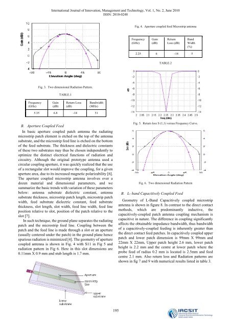
Fig. 4. Aperture coupled feed <strong>Microstrip</strong> antenna<br />
Frequency<br />
(GHz)<br />
Gain<br />
(dB)<br />
TABLE.2<br />
Return<br />
Loss (dB)<br />
A. Aperture Coupled Feed<br />
Band<br />
Width<br />
(%)<br />
2.25 6 -14 5<br />
Fig. 5. Return loss S (1,1) versus Frequency Curve.<br />
Fig. 6. Two dimensional Radiation Pattern<br />
B. L- band Capacitively Coupled Feed<br />
Geometry <strong>of</strong> L-Band Capacitively coupled microstrip<br />
antenna is shown in figure 8. In contrast to the direct contact<br />
methods, which are predominantly inductive, the<br />
capacitively-coupled patch antenna coupling mechanism is<br />
capacitive in nature. The difference in coupling significantly<br />
affects the obtainable impedance bandwidth, thus bandwidth<br />
<strong>of</strong> a capacitively-coupled feeding is inherently greater than<br />
the direct contact feed patches. In capacitively coupled upper<br />
patch and lower patch dimension is 99mm X 99mm and<br />
22mm X 22mm, Upper patch height 2.6 mm, lower patch<br />
height is 2.2 mm and the centre at lower patch where the<br />
probe feed <strong>of</strong> radius 0.2 mm is located is 2.5mm and feed<br />
centre 2.1 mm. Also return loss and Radiation patterns are<br />
shown in fig 7 and 9 with numerical results listed in table 3.