Low Noise Figure of Cascaded LNA at 5.8 GHz Using T ... - ijimt
Low Noise Figure of Cascaded LNA at 5.8 GHz Using T ... - ijimt
Low Noise Figure of Cascaded LNA at 5.8 GHz Using T ... - ijimt
Create successful ePaper yourself
Turn your PDF publications into a flip-book with our unique Google optimized e-Paper software.
Intern<strong>at</strong>ional Journal <strong>of</strong> Innov<strong>at</strong>ion, Management and Technology, Vol. 3, No. 6, December 2012<br />
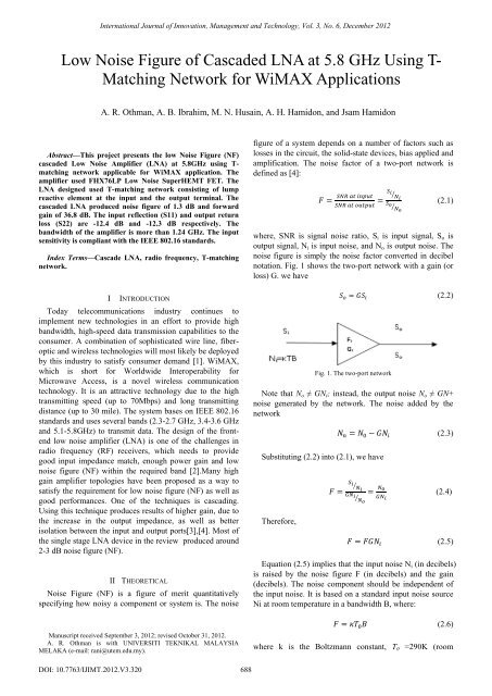
<strong>Low</strong> <strong>Noise</strong> <strong>Figure</strong> <strong>of</strong> <strong>Cascaded</strong> <strong>LNA</strong> <strong>at</strong> <strong>5.8</strong> <strong>GHz</strong> <strong>Using</strong> T-<br />
M<strong>at</strong>ching Network for WiMAX Applic<strong>at</strong>ions<br />
A. R. Othman, A. B. Ibrahim, M. N. Husain, A. H. Hamidon, and Jsam Hamidon<br />
<br />
Abstract—This project presents the low <strong>Noise</strong> <strong>Figure</strong> (NF)<br />
cascaded <strong>Low</strong> <strong>Noise</strong> Amplifier (<strong>LNA</strong>) <strong>at</strong> <strong>5.8</strong><strong>GHz</strong> using T-<br />
m<strong>at</strong>ching network applicable for WiMAX applic<strong>at</strong>ion. The<br />
amplifier used FHX76LP <strong>Low</strong> <strong>Noise</strong> SuperHEMT FET. The<br />
<strong>LNA</strong> designed used T-m<strong>at</strong>ching network consisting <strong>of</strong> lump<br />
reactive element <strong>at</strong> the input and the output terminal. The<br />
cascaded <strong>LNA</strong> produced noise figure <strong>of</strong> 1.3 dB and forward<br />
gain <strong>of</strong> 36.8 dB. The input reflection (S11) and output return<br />
loss (S22) are -12.4 dB and -12.3 dB respectively. The<br />
bandwidth <strong>of</strong> the amplifier is more than 1.24 <strong>GHz</strong>. The input<br />
sensitivity is compliant with the IEEE 802.16 standards.<br />
Index Terms—Cascade <strong>LNA</strong>, radio frequency, T-m<strong>at</strong>ching<br />
network.<br />
I<br />
INTRODUCTION<br />
Today telecommunic<strong>at</strong>ions industry continues to<br />
implement new technologies in an effort to provide high<br />
bandwidth, high-speed d<strong>at</strong>a transmission capabilities to the<br />
consumer. A combin<strong>at</strong>ion <strong>of</strong> sophistic<strong>at</strong>ed wire line, fiberoptic<br />
and wireless technologies will most likely be deployed<br />
by this industry to s<strong>at</strong>isfy consumer demand [1]. WiMAX,<br />
which is short for Worldwide Interoperability for<br />
Microwave Access, is a novel wireless communic<strong>at</strong>ion<br />
technology. It is an <strong>at</strong>tractive technology due to the high<br />
transmitting speed (up to 70Mbps) and long transmitting<br />
distance (up to 30 mile). The system bases on IEEE 802.16<br />
standards and uses several bands (2.3-2.7 <strong>GHz</strong>, 3.4-3.6 <strong>GHz</strong><br />
and 5.1-<strong>5.8</strong><strong>GHz</strong>) to transmit d<strong>at</strong>a. The design <strong>of</strong> the frontend<br />
low noise amplifier (<strong>LNA</strong>) is one <strong>of</strong> the challenges in<br />
radio frequency (RF) receivers, which needs to provide<br />
good input impedance m<strong>at</strong>ch, enough power gain and low<br />
noise figure (NF) within the required band [2].Many high<br />
gain amplifier topologies have been proposed as a way to<br />
s<strong>at</strong>isfy the requirement for low noise figure (NF) as well as<br />
good performances. One <strong>of</strong> the techniques is cascading.<br />
<strong>Using</strong> this technique produces results <strong>of</strong> higher gain, due to<br />
the increase in the output impedance, as well as better<br />
isol<strong>at</strong>ion between the input and output ports[3],[4]. Most <strong>of</strong><br />
the single stage <strong>LNA</strong> device in the review produced around<br />
2-3 dB noise figure (NF).<br />
II THEORETICAL<br />
<strong>Noise</strong> <strong>Figure</strong> (NF) is a figure <strong>of</strong> merit quantit<strong>at</strong>ively<br />
specifying how noisy a component or system is. The noise<br />
Manuscript received September 3, 2012; revised October 31, 2012.<br />
A. R. Othman is with UNIVERSITI TEKNIKAL MALAYSIA<br />
MELAKA (e-mail: rani@utem.edu.my).<br />
figure <strong>of</strong> a system depends on a number <strong>of</strong> factors such as<br />
losses in the circuit, the solid-st<strong>at</strong>e devices, bias applied and<br />
amplific<strong>at</strong>ion. The noise factor <strong>of</strong> a two-port network is<br />
defined as [4]:<br />
(2.1)<br />
where, SNR is signal noise r<strong>at</strong>io, S i is input signal, S o is<br />
output signal, N i is input noise, and N o is output noise. The<br />
noise figure is simply the noise factor converted in decibel<br />
not<strong>at</strong>ion. Fig. 1 shows the two-port network with a gain (or<br />
loss) G. we have<br />
Fig. 1. The two-port network<br />
(2.2)<br />
Note th<strong>at</strong> N o ≠ GN i ; instead, the output noise N o ≠ GN+<br />
noise gener<strong>at</strong>ed by the network. The noise added by the<br />
network<br />
Substituting (2.2) into (2.1), we have<br />
Therefore,<br />
(2.3)<br />
(2.4)<br />
(2.5)<br />
Equ<strong>at</strong>ion (2.5) implies th<strong>at</strong> the input noise N i (in decibels)<br />
is raised by the noise figure F (in decibels) and the gain<br />
(decibels). The noise component should be independent <strong>of</strong><br />
the input noise. It is based on a standard input noise source<br />
Ni <strong>at</strong> room temper<strong>at</strong>ure in a bandwidth B, where:<br />
(2.6)<br />
where k is the Boltzmann constant, T 0 =290K (room<br />
DOI: 10.7763/IJIMT.2012.V3.320<br />
688
Intern<strong>at</strong>ional Journal <strong>of</strong> Innov<strong>at</strong>ion, Management and Technology, Vol. 3, No. 6, December 2012<br />
temper<strong>at</strong>ure), and B is the bandwidth (MHz). Then,<br />
equ<strong>at</strong>ion (2.4) becomes<br />
(2.7)<br />
For a cascaded circuit with n element as shown Fig. 2;<br />
the overall noise factor can be found from the noise factor<br />
and gains <strong>of</strong> the individual element [4].<br />
Fig. 2: <strong>Cascaded</strong> circuit with n network<br />
The overall noise figure F is:<br />
(2.8)<br />
Equ<strong>at</strong>ion 2.5 allows for the calcul<strong>at</strong>ion <strong>of</strong> the noise figure<br />
<strong>of</strong> a general cascaded system. From eq. (2.8), it is clear th<strong>at</strong><br />
the gain and noise figure in the first stage are critical in<br />
achieving a low overall noise figure. It is very desirable to<br />
have a low noise figure and high gain in the first stage. To<br />
use Equ<strong>at</strong>ion (2.8), all F’s and G’s are in r<strong>at</strong>io. For a passive<br />
component with loss L in r<strong>at</strong>io, we will have G = 1/L and F<br />
= L.<br />
Note th<strong>at</strong>, F=F 1 due to the high gain in the first stage. The<br />
first-stage amplifier noise figure domin<strong>at</strong>es the overall noise<br />
figure. One would like to select the first RF amplifier with a<br />
low noise figure and a high gain to ensure the low noise<br />
figure for the overall system.<br />
The equivalent noise temper<strong>at</strong>ure is defined as<br />
(2.9)<br />
where T 0 =290K (room temper<strong>at</strong>ure) and F in r<strong>at</strong>io; therefore<br />
(2.10)<br />
For a cascaded circuit shown as Fig. 3, equ<strong>at</strong>ion (2.8) can<br />
be rewritten as<br />
(2.11)<br />
where, T e is the overall equivalent noise temper<strong>at</strong>ure in<br />
Kelvin.<br />
Fig. 3. <strong>Noise</strong> temper<strong>at</strong>ure for a cascaded circuit<br />
The noise temper<strong>at</strong>ure is useful for noise factor<br />
calcul<strong>at</strong>ions involving an antenna for example, if an antenna<br />
noise temper<strong>at</strong>ure is T A , the overall system noise including<br />
the antenna is<br />
(2.12)<br />
where, T e is overall cascaded circuit noise temper<strong>at</strong>ure.<br />
As pointed out earlier the antenna noise temper<strong>at</strong>ure is<br />
approxim<strong>at</strong>ely equal to 290K for an antenna pointing to<br />
earth. The antenna noise temper<strong>at</strong>ure could be very low (a<br />
few Kelvin) for an antenna pointing to the sky [4].<br />
The design specific<strong>at</strong>ions for the cascaded <strong>LNA</strong> were<br />
shown in Table I:<br />
TABLE I: DESIGN SPECIFICATION FOR <strong>LNA</strong><br />
III<br />
<strong>LNA</strong> CIRCUIT DESIGN<br />
The <strong>Cascaded</strong> <strong>LNA</strong> was design with advanced Design<br />
System (ADS 2008) with 2 Volts (V DS ) and 10mA <strong>of</strong> bias<br />
current was supply. The overall performance <strong>of</strong> the low<br />
noise amplifier is determined by calcul<strong>at</strong>ing the transducer<br />
gain G T , noise figure F and the input and output standing<br />
wave r<strong>at</strong>ios, VSWR IN and VSWR OUT . The optimum , Γ<br />
and<br />
<strong>Cascaded</strong> <strong>LNA</strong><br />
Gain dB > 35<br />
Frequency<br />
<strong>5.8</strong> <strong>GHz</strong><br />
NF dB < 3<br />
M<strong>at</strong>ching Technique Π Network & Microstrip + Lump<br />
reactive element<br />
VSWR 1.5<br />
Bandwidth MHz<br />
>1000(<strong>5.8</strong> <strong>GHz</strong> Centre)<br />
Input sensitivity<br />
- 80 dBm<br />
Γ were obtained as<br />
L<br />
Γ<br />
opt<br />
= 17.354 +j 50.131 and<br />
opt<br />
= 79.913- j7.304. The calcul<strong>at</strong>ed gain for the <strong>LNA</strong> was 17<br />
dB, which correspond to a noise figure <strong>of</strong> 0.301 dB. The<br />
input m<strong>at</strong>ching load Γ is required to provide highloaded<br />
Q factor for better sensitivity. A T-network was used<br />
to m<strong>at</strong>ch the input impedance. The elements <strong>of</strong> T-network<br />
can be realized in the form <strong>of</strong> lump reactive elements and<br />
microstrip line impedance. For the output impedance Z L ,<br />
since the impedance is real, suitable m<strong>at</strong>ching for the load is<br />
by using a quarter-wave transformer [6], [8].The quarterwave<br />
transformers convert the complex impedance into real<br />
impedance.<br />
<strong>Using</strong> Smith Chart m<strong>at</strong>ching technique, the component<br />
values are shown in Table II. The DC block capacitor was<br />
selected for the circuit and the value is recommended <strong>at</strong><br />
least 10 times from the C 1 . For this reason 7.5 pF capacitors<br />
are selected as bypass capacitors. With these components,<br />
the schem<strong>at</strong>ic circuit for single stage <strong>LNA</strong> is shown in Fig.<br />
4. From equ<strong>at</strong>ion (2.1) to (2.12), the rel<strong>at</strong>ed noise figure and<br />
gain <strong>of</strong> the amplifier were calcul<strong>at</strong>ed. By using ADS 2008,<br />
the noise figure circle was obtained in the unit circle and the<br />
opt<br />
Γ<br />
L<br />
689
VSWR recorded was 2.179.<br />
Intern<strong>at</strong>ional Journal <strong>of</strong> Innov<strong>at</strong>ion, Management and Technology, Vol. 3, No. 6, December 2012<br />
Fig. 4. Single stage <strong>LNA</strong><br />
TABLE II: <strong>LNA</strong> PARAMETERS<br />
Components<br />
L 1<br />
L 2<br />
L 3<br />
L 4<br />
C 1<br />
C B<br />
Values<br />
3.60 nH<br />
0.88 nH<br />
0.67 nH<br />
0.75 nH<br />
0.5 pF<br />
7.5 pF<br />
Fig. 6. (b). <strong>Noise</strong> figure and stability for single <strong>LNA</strong><br />
Fig. 5 shows the cascaded amplifier, this is realized from<br />
two single stages amplifiers. To achieve the targeted overall<br />
gain <strong>of</strong> 35 dB, it was decided to design a cascaded amplifier<br />
using similar stages to double the <strong>LNA</strong> gain. The<br />
components <strong>of</strong> m<strong>at</strong>ching are similar with single <strong>LNA</strong> but<br />
the L 4 =0.67nH, L 5 =0.88nH and C 2 =0.5pF was inserted. It is<br />
call inter-stage m<strong>at</strong>ching network.<br />
Fig. 6. (c). S-parameter for cascaded <strong>LNA</strong><br />
Fig. 5. <strong>Cascaded</strong> <strong>LNA</strong><br />
IV<br />
SIMULATION RESULT<br />
The simul<strong>at</strong>ed cascaded amplifiers results are shown in<br />
Table III. These values were within the design specific<strong>at</strong>ion<br />
and were accepted. The graph outputs S-parameter are<br />
shown in Fig. 6. (a), Fig. 6. (b), Fig. 6. (c) and Fig. 6. (d).<br />
Fig. 6. (d). <strong>Noise</strong> figure and stability for cascaded <strong>LNA</strong><br />
TABLE III: S-PARAMETER RESULTS FOR <strong>LNA</strong><br />
<strong>LNA</strong>/dB S 11 S 12 S 21 S 22 NF (K)<br />
Single -12.8 -20.2 18.2 -27.9 0.747 1.023<br />
<strong>Cascaded</strong> -22.5 -40.4 36.1 -37.6 1.171 1.492<br />
Fig. 6. (a). S-parameter for single <strong>LNA</strong><br />
V<br />
MEASUREMENT<br />
Before recording all measurements, a standard procedure<br />
<strong>of</strong> calibr<strong>at</strong>ion is followed to ensure th<strong>at</strong> the measurement<br />
tools were calibr<strong>at</strong>ed. Fig. 7 shows the power output versus<br />
frequency for <strong>Cascaded</strong> amplifier. It is also tested for their<br />
frequency response. The signal gener<strong>at</strong>or output is set to -80<br />
690
Intern<strong>at</strong>ional Journal <strong>of</strong> Innov<strong>at</strong>ion, Management and Technology, Vol. 3, No. 6, December 2012<br />
dBm according to IEEE 802.16 standard. The amplifier<br />
produced 36.8 dB and the output <strong>of</strong> the amplifier measured<br />
is -43.2 dBm with bandwidth more than 1.24 <strong>GHz</strong>. Fig. 8<br />
shows the noise figure measured for cascaded amplifier.<br />
The <strong>Noise</strong> <strong>Figure</strong> (NF) is measured using noise figure setup.<br />
It observed th<strong>at</strong> the NF <strong>of</strong> the simul<strong>at</strong>ed analysis is 1.17 dB<br />
and the experimental value is 1.3 dB.<br />
VI<br />
CONCLUSION<br />
A <strong>Cascaded</strong> <strong>LNA</strong> has been simul<strong>at</strong>ed and developed<br />
successfully with IEEE standard 802.16 WiMAX. It is<br />
observed th<strong>at</strong> the simul<strong>at</strong>ed and experiment results have not<br />
much different. It is important to take note when designing<br />
the amplifier to m<strong>at</strong>ch the amplifier circuits. The <strong>5.8</strong><strong>GHz</strong><br />
<strong>LNA</strong> has been developed successfully and the circuit<br />
contributed to the front end receiver <strong>at</strong> the described<br />
frequency. For better performance in gain <strong>of</strong> the amplifier,<br />
it can be achieved by increasing the number <strong>of</strong> stages to<br />
improve the gain and noise figure <strong>of</strong> the design. Higher gain<br />
would expand the coverage or communic<strong>at</strong>ion distance.<br />
Fig. 7. Power output vs frequency (cascaded)<br />
REFERENCES<br />
[1] C. W. Chang and Z. Lin, “A 1V 14.6dB Gain <strong>LNA</strong> for WIMAX 2 – 6<br />
<strong>GHz</strong> Applic<strong>at</strong>ion,” IEEE Proceeding, 2009.<br />
[2] R. Wang, S. Chen, C. Huang, C. Lie, and Y. Lin, “2-6 <strong>GHz</strong> Current-<br />
Reused <strong>LNA</strong> With Transformer-type Inductors,” IEEE Proceeding,<br />
2008.<br />
[3] M. A. G. Lorenzo and M. T. G. de Leon, “Comparison <strong>of</strong> <strong>LNA</strong><br />
Topology for Wimax Applic<strong>at</strong>ion in a Standard 90-nm CMOS<br />
Process,” 12th Intern<strong>at</strong>ional Conference on Computer Modelling and<br />
Simul<strong>at</strong>ion, pp-642-647, 2010.<br />
[4] K. Chang, I. Bahl, and V. Nair, Rf and Microwave Circuit for<br />
Wireless Systems, 2009.<br />
[5] D. Ayadi, S. Rodriguez, M. Loulou, and M. Ismail, “System Level<br />
Design <strong>of</strong> Radio Frequency Receiver for IEEE 802.16 Standard,”<br />
IEEE Proceeding, 2009.<br />
[6] I. Bahl and P. Bhartia, Microwave Solid St<strong>at</strong>e Circuit Design, 2nd Ed.,<br />
2003.<br />
[7] R. C. Li, RF Circuit Design, 2009.<br />
[8] I. J. Bahl, Fundamentals <strong>of</strong> RF and Microwave Transistor Amplifier,<br />
2009.<br />
[9] A. Baishya, P. P. Sahu, and M. K. Naskar, “A High Gain <strong>Low</strong> <strong>Noise</strong><br />
Amplifier for 0.9 – 6<strong>GHz</strong> Wireless Applic<strong>at</strong>ion,” IEEE Proceeding,<br />
2011.<br />
Fig. 8. <strong>Noise</strong> figure (cascaded)<br />
691


