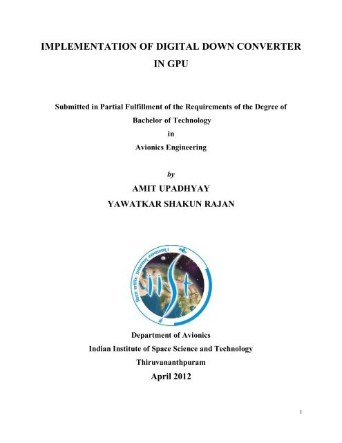
IMPLEMENTATION OF DIGITAL DOWN CONVERTER IN GPU
IMPLEMENTATION OF DIGITAL DOWN CONVERTER IN GPU
IMPLEMENTATION OF DIGITAL DOWN CONVERTER IN GPU

Create successful ePaper yourself
Turn your PDF publications into a flip-book with our unique Google optimized e-Paper software.
<strong>IMPLEMENTATION</strong> <strong>OF</strong> <strong>DIGITAL</strong> <strong>DOWN</strong> <strong>CONVERTER</strong><br />
<strong>IN</strong> <strong>GPU</strong><br />
Submitted in Partial Fulfillment of the Requirements of the Degree of<br />
Bachelor of Technology<br />
in<br />
Avionics Engineering<br />
by<br />
AMIT UPADHYAY<br />
YAWATKAR SHAKUN RAJAN<br />
Department of Avionics<br />
Indian Institute of Space Science and Technology<br />
Thiruvananthpuram<br />
April 2012<br />
I
BONAFIDE CERTIFICATE<br />
This is to certify that this project report entitled “<strong>IMPLEMENTATION</strong> <strong>OF</strong><br />
<strong>DIGITAL</strong> <strong>DOWN</strong> CONVERSION <strong>IN</strong> <strong>GPU</strong>” submitted to Indian Institute of<br />
Space Science and Technology, Thiruvananthapuram, is a bonafide record of<br />
work done by Amit Upadhyay and Yawatkar Shakun Rajan under my<br />
supervision at the Giant Metrewave Radio Telescope, NCRA-TIFR from “9 th<br />
January 2012” to “27 th April 2012”.<br />
Mr. Ajith Kumar<br />
Head, Digital Backend,<br />
GMRT, NCRA-TIFR<br />
Dr. Yashwant Gupta<br />
Chief Scientist,<br />
GMRT,NCRA-TIFR<br />
Place: GMRT, Khodad<br />
Date: 27/04/2012<br />
II
DECLARATION BY AUTHORS<br />
This is to declare that this report has been written by us. No part of the report<br />
is plagiarized from other sources. All information included from other sources has<br />
been duly acknowledged. We aver that if any part of the report is found to be<br />
plagiarized, we are shall take full responsibility for it.<br />
Amit Upadhyay<br />
Roll No.:SC08B058<br />
Yawatkar Shakun Rajan<br />
Roll No.:SC08B040<br />
Place: GMRT, Khodad<br />
Date: 27/04/2012<br />
III
ACKNOWLEDGEMENT<br />
We thank Dr. Yashwant Gupta, Chief Scientist, GMRT, for sparing his valuable time to<br />
help us understand various aspects of this project and for guiding us to the successful completion<br />
of the project.<br />
We express our gratitude to Mr. Ajith Kumar, Head, Digital Backend Systems, GMRT,<br />
for facilitating this project and also for all help in support rendered.<br />
We wholeheartedly thank Mr. Harshvardhan Reddy, Engineer C [FTA], GMRT for<br />
spending his quality time helping us to complete this project.<br />
We also place on record our thanks to Dr. S. K. Ghosh, Centre Director NCRA and Dr.<br />
K.S. Dasgupta, Director IIST for giving us such a great opportunity by arranging this internship<br />
program.<br />
Finally, we sincerely thank all people, who have helped us during the project, directly or<br />
indirectly.<br />
April 2012<br />
Amit Upadhyay<br />
Yawatkar Shakun Rajan<br />
IV
ABSTRACT<br />
Giant Metrewave Radio Telescope is undergoing an upgradation. GMRT is mainly used for<br />
pulsar, continuum and spectral line observations. Spectral Line observations require more resolution<br />
which can be achieved by narrowband mode. Thus to utilize the GMRT correlator resources efficiently<br />
and to speed up the further signal processing, Digital Down Converter is of great use. Digital Down<br />
Conversion down-converts the desired band to baseband resulting into the increased resolution of signal.<br />
The limited FFT size can be utilized to get more resolution of signal. Graphic Processing Unit (<strong>GPU</strong>)<br />
decreases the time of various operations in DDC significantly. Hence, the DDC design is done in <strong>GPU</strong><br />
The project work includes the design of DDC block in <strong>GPU</strong> using a programming tool Compute Unified<br />
Device Architecture C (CUDA-C). All the sub blocks of DDC were designed and combined to form<br />
DDC. The block was tested for the CW signal and also the channel noise signal; it showed the desired<br />
down-conversion of the band to baseband. DDC block also increases resolution of the signal. It decimates<br />
the output and spreads it over all the channels. It reduces the data rate in the GMRT correlator program to<br />
a great extent. The timing analysis of the DDC block was done with and without using shared memory of<br />
the <strong>GPU</strong>. Using shared memory is beneficial as far as the convolution time is considered. When the same<br />
code for DDC was run on CPU, it was observed that <strong>GPU</strong> gives about 250 times enhancement in the time<br />
consumed. The design of the DDC block was integrated with the existing GMRT Correlator program. It<br />
was placed just before the FFT block. Local GMRT software „TAX‟ was used to visualize the outputs<br />
obtained from the program. The desired down converted band was observed with the increased resolution.<br />
The GMRT Correlator program along with the DDC block has been further modified as per the<br />
requirements of Phase Correction and MAC block of the GMRT Correlator design. It enabled us for the<br />
sky testing of the GMRT Correlator program with the DDC feature. The sky test results were obtained<br />
and verified successfully.<br />
V
TABLE <strong>OF</strong> CONTENTS<br />
BONAFIDE CERTIFICATE……………..……………………………………………………….......II<br />
DECLARATION BY AUTHORS….…………………………………………………..……………III<br />
ACKNOWLEDGEMENT…………….…………………………….…………...…………...……....IV<br />
ABSTRACT……………………………….……………………………..……….………………..….V<br />
TABLE <strong>OF</strong> CONTENTS…………………….……………………………………..……...………...VI<br />
LIST <strong>OF</strong> FIGURES…………………………….…………..………………………........................VIII<br />
LIST <strong>OF</strong> TABLES………………………………….………………………………..………………..X<br />
LIST <strong>OF</strong> ABBREVIATIONS………………………….……………………………...…………......XI<br />
1. <strong>IN</strong>TRODUCTION..............................................................................................................................1<br />
1.1. Organization Profile: ...................................................................................................................1<br />
1.2 GMRT correlator system upgrade: ...............................................................................................2<br />
1.3 Need for Digital Down Converter in <strong>GPU</strong> ...................................................................................3<br />
2. <strong>GPU</strong> AND CUDA-C .........................................................................................................................4<br />
2.1 Graphic Processing Unit (<strong>GPU</strong>) ...................................................................................................4<br />
2.2 CUDA C (Compute Unified Device Architecture) ......................................................................6<br />
3. <strong>DIGITAL</strong> <strong>DOWN</strong> <strong>CONVERTER</strong> .......................................................................................………10<br />
3.1 How a DDC works: .......................................................................................................……….10<br />
3.2 Advantages of using DDC over analog techniques: ...................................................................14<br />
3.3 Disadvantages of using DDC: ................................................................................................... 15<br />
4. AIM AND OBJECTIVE ..................................................................................................................16<br />
4.1 Objectives of the Project .............................................................................................................16<br />
4.2 Problem Definition .....................................................................................................................16<br />
4.3 Project Plan .................................................................................................................................16<br />
VI
5. DDC BLOCK DESIGN .................................................................................................................. 17<br />
5.1 Local Oscillator ......................................................................................................................... 17<br />
5.2 Mixer ………............................................................................................................................. 18<br />
5.3 Low Pass Filter........................................................................................................................... 18<br />
5.4 Decimator .................................................................................................................................. 18<br />
5.5 Complex to Complex FFT ......................................................................................................... 18<br />
5.6 Frequency Domain Visualization of working of DDC Block ................................................... 18<br />
6. <strong>IN</strong>TEGRATION <strong>OF</strong> DDC BLOCK WITH GMRT CORRELATOR PROGRAM….................... 22<br />
6.1 Brief explanation of GMRT correlator code.............................................................................. 22<br />
6.2 Adding DDC feature to GMRT correlator ……........................................................................ 22<br />
6.3 Sky Test of GMRT Correlator Program Featured With DDC…………………………………23<br />
7. Results and Discussions………………........................................................................................... 24<br />
8. TIM<strong>IN</strong>G ANALYSIS: .................................................................................................................... 41<br />
8.1 Convolution Timing analysis: ................................................................................................... 42<br />
8.2 Improvement Factor between Convolution timings of <strong>GPU</strong> and CPU ......................................42<br />
8.3 Improvement Factor between Convolution timings of <strong>GPU</strong> when using <strong>GPU</strong> shared<br />
memory and without using <strong>GPU</strong> shared memory... .................................................................. 43<br />
9. CONCLUSION .............................................................................................................................. 44<br />
10. FUTURE SCOPE AND RECOMMENDATIONS....................................................................... 45<br />
9. REFERENCES ............................................................................................................................... 46<br />
APPENDIX – I.................................................................................................................................... 47<br />
APPENDIX – II ................................................................................................................................. 48<br />
APPENDIX – III..................................................................................................................................51<br />
APPENDIX – IV................................................................................................................................. 52<br />
APPENDIX – V...................................................................................................................................55<br />
APPENDIX –VI..........................................................................................................................…….56<br />
APPENDIX –VII.........................................................................................................................…….57<br />
APPENDIX –VI..........................................................................................................................…….58<br />
APPENDIX –IX..........................................................................................................................…….60<br />
VII
LIST <strong>OF</strong> FIGURES<br />
Figure 2-1 Graphic Processing Unit......................................................................................................5<br />
Figure 2-2 Fundamental architecture design difference between CPUs and <strong>GPU</strong>s .............................5<br />
Figure 2-3 CUDA memory architecture (LEFT); CUDA Thread organization (RIGHT) ...................9<br />
Figure 3-1 A theoretical DDC Block Design ............................................................................. 11<br />
Figure 3-2 spectrum of a continuous analog signal .................................................................... 11<br />
Figure 3-3 Spectrum of digitized signal Sample frequency Fs ................................................... 11<br />
Figure 3-4 Spectrum of digitized signal after mixing sample frequency Fs ................................ 12<br />
Figure 3-5 Low pass digital filter frequency response Sample frequency Fs .............................. 12<br />
Figure 3-6 Spectrum of digitized signal after filtering Sample Frequency Fs ............................. 13<br />
Figure 3-7 Spectrum of Qudrature signal after decimation Sample Frequency Fs/7 ................... 13<br />
Figure 3-8 Complex Frequency domain view ............................................................................ 14<br />
Figure 5-1 Position of DDC block in GMRT Correlator ............................................................ 17<br />
Figure 5-2 DDC Block Description ........................................................................................... 17<br />
Figure 5-3 Obtaining In-Phase Signal ........................................................................................ 19<br />
Figure 5-4 Mixing Operation of Input Signal and Sine Wave in Frequency Domain .................. 19<br />
Figure 5-5 Obtaining Quadrature Phase Signal .......................................................................... 20<br />
Figure 5-6 Addition of In-Phase and Quadrature Phase Signals ................................................. 20<br />
Figure 5-7 LPF Operation ......................................................................................................... 21<br />
Figure 7-1 DDC Input and output; LO 0MHz, DF 1, Taps 21 .......................................................... 24<br />
Figure 7-2 DDC Input and Output; LO 10 MHz, DF 2, Taps 21 ...................................................... 25<br />
Figure 7-3 DDC Input and Output; LO 50MHz, DF 8, Taps 21 ....................................................... 25<br />
Figure 7-4 DDC Input and Output; LO 20 MHz, DF 4, Taps 21 ...................................................... 26<br />
Figure 7-5 Plot showing output of GMRT correlator viewed using TAX tool;<br />
LO Freq = 0MHz and Decimation Factor = 1....................................................................28<br />
Figure 7-6 Plot showing output of GMRT correlator viewed using TAX tool;<br />
LO Freq = 0MHz and Decimation Factor = 2....................................................................28<br />
Figure 7-7 Plot showing output of GMRT correlator viewed using TAX tool;<br />
LO Freq = 0MHz and Decimation Factor = 4................................................................... 29<br />
Figure 7-8 Plot showing output of GMRT correlator viewed using TAX tool;<br />
LO Freq = 10MHz and Decimation Factor = 1......................................................................30<br />
VIII
Figure 7-9 Plot showing output of GMRT correlator viewed using TAX tool;<br />
LO Freq = 30MHz and Decimation Factor = 1..................................................................30<br />
Figure 7-10 Plot showing output of GMRT correlator viewed using TAX tool;<br />
LO Freq = 80MHz and Decimation Factor = 1............................................................... 31<br />
Figure 7-11 Plot showing output of GMRT correlator viewed using TAX tool;<br />
LO Freq = 10MHz and Decimation Factor = 2............................................................... 32<br />
Figure 7-12 Plot showing output of GMRT correlator viewed using TAX tool;<br />
LO Freq = 30MHz and Decimation Factor = 2............................................................... 32<br />
Figure 7-13 Plot showing output of GMRT correlator viewed using TAX tool;<br />
LO Freq = 30MHz and Decimation Factor = 4............................................................... 33<br />
Figure 7-14 Plot showing output of GMRT correlator viewed using TAX tool;<br />
LO Freq = 30MHz and Decimation Factor = 8............................................................... 33<br />
Figure 7-15 Plot showing output of GMRT correlator viewed using TAX tool;<br />
LO Freq = 80MHz and Decimation Factor = 4............................................................... 34<br />
Figure 7-16 Self Correlation; DF 1, LO 0MHz, Taps 15 ................................................................... 35<br />
Figure 7-17 Cross Correlation; DF 1, LO 0MHz, Taps 15................................................................. 35<br />
Figure 7-18 Timestamp Cross Correlation; Channel 75, DF 1, LO 0MHz, Taps 15.......................... 36<br />
Figure 7-19 Self Correlation; DF 2, LO 10MHz, Taps 15.................................................................. 37<br />
Figure 7-20 Cross Correlation; DF 2, LO 10MHz, Taps 15 ............................................................... 37<br />
Figure 7-21 Timestamp Cross Correlation; Channel 200, DF 2, LO 10MHz, Taps 15 ......................38<br />
Figure 7-22 Self Correlation; DF 4, LO 50MHz, Taps 15.................................................................. 39<br />
Figure 7-23 Cross Correlation; DF 4, LO 50MHz, Taps 15 ............................................................... 39<br />
Figure 7-24 Timestamp Cross Correlation; Channel 200, DF 4, LO 50MHz, Taps 15 ..................... 40<br />
Figure 8-1 Convolution Time for <strong>GPU</strong> with and without<br />
using <strong>GPU</strong> shared memory and Convolution time for CPU............................................................... 42<br />
Figure 8-2 Improvement factor between <strong>GPU</strong> convolution timings<br />
and CPU convolution timings............................................................................................. 42<br />
Figure 8-3 Improvement factor between <strong>GPU</strong> timings while using shared <strong>GPU</strong> memory<br />
and while not using <strong>GPU</strong> shared memory for various cases recorded in table............ 43<br />
IX
LIST <strong>OF</strong> TABLES<br />
Table 7.1 Contains the Convolution Time for <strong>GPU</strong> with and without using <strong>GPU</strong> shared memory and<br />
Convolution time for CPU by varying various parameters………………………………………………..35<br />
X
LIST <strong>OF</strong> ABBREVIATIONS<br />
ADC<br />
ALU<br />
ANSI<br />
API<br />
CPU<br />
CUDA<br />
CW<br />
DDC<br />
FFT<br />
FIR<br />
GMRT<br />
<strong>GPU</strong><br />
HPC<br />
LO<br />
LPF<br />
MAC<br />
NCRA<br />
NVCC<br />
RF<br />
TAX<br />
Analog to Digital Converter<br />
Arithmetic Logic Unit<br />
American National Standards Institute<br />
Application Program Interface<br />
Central Processing Unit<br />
Compute Unified Device Architecture<br />
Continuous Wave<br />
Digital Down Converter<br />
Fast Fourier Transform<br />
Finite Impulse Response<br />
Giant Metrewave Radio Telescope<br />
Graphic Processing Unit<br />
High Performance Computing<br />
Local Oscillator<br />
Low Pass Filter<br />
Multiplication And Accumulation<br />
National Centre for Radio Astrophysics<br />
NVIDIA CUDA C Compiler<br />
Radio Frequency<br />
TK Assisted Xstract<br />
XI
1. <strong>IN</strong>TRODUCTION<br />
1.1. Organization Profile:<br />
National Centre for Radio Astrophysics has set up a unique facility for radio astronomical<br />
research using the metre wavelengths range of the radio spectrum, known as the Giant<br />
Metrewave Radio Telescope (GMRT), it is located at a site about 80 km north of Pune. GMRT<br />
consists of 30 fully steerable gigantic parabolic dishes of 45m diameter each spread over<br />
distances of up to 25 km. GMRT is one of the most challenging experimental programs in basic<br />
sciences undertaken by Indian scientists and engineers. GMRT is an interferometer which uses a<br />
technique named Aperture Synthesis [2] to make images of radio sources in sky.<br />
The number and configuration of the dishes was optimized to meet the principal<br />
astrophysical objectives which require sensitivity at high angular resolution as well as ability to<br />
image radio emission from diffuse extended regions [8] . Fourteen of the thirty dishes are located<br />
more or less randomly in a compact central array in a region of about 1 sq. km. The remaining<br />
sixteen dishes are spread out along the 3 arms of an approximately `Y'-shaped configuration over<br />
a much larger region, with the longest interferometry baseline of about 25 km. The multiplication<br />
or correlation of radio signals from all the 435 possible pairs of antennas or interferometers over<br />
several hours will thus enable radio images of celestial objects to be synthesized with a<br />
resolution equivalent to that obtainable with a single gigantic dish 25 kilometers in diameter!<br />
- Telescope works at long wavelengths 21cm and longer.<br />
- Each antenna has 4 different receivers mounted at focus and each individual receiver<br />
assembly can rotate so that the user can select the frequency at which to observe.<br />
- GMRT operates in frequency bands centered at:153 MHz, 233 MHz, 327 MHz, 610<br />
MHz and 1420 MHz<br />
- The GMRT Correlator is an FX [2] correlator.<br />
1
1.2 GMRT correlator system upgrade:<br />
The goal of GMRT correlator upgrade is to provide continuous spectral coverage and better<br />
spectral resolution. The new upgrade of GMRT correlator system aims at continuous coverage<br />
from 100MHz-1600MHz. The current system has only 32MHz of maximum bandwidth which is<br />
aimed to be improved up to 400MHz.<br />
The GMRT correlator will provide wideband coverage for radio astronomy applications<br />
namely, continuum observation, pulsar observation and spectral line observation. This wideband<br />
coverage upgrade also leads to the need for using a DDC system because if narrowband<br />
observations are to be made the 400MHz bandwidth should be down converted to required<br />
baseband frequency. The addition of DDC will also reduce the data rate because of the<br />
decimation performed by DDC block. The narrowband observations are usually done for spectral<br />
line analysis of any radio source.<br />
The FFT size used in current GMRT correlator system is 2048 or 2K i.e. 1024 frequency<br />
channels. Thus the current spectral resolution is 32/1024 MHz. The GMRT correlator will be<br />
upgraded to perform 4K FFT i.e. 2048 frequency channels which will make the spectral<br />
resolution as 400/4096 MHz which is enhanced as compared to current GMRT correlator system.<br />
2
1.3 Need for Digital Down Converter in <strong>GPU</strong><br />
Digital Down Conversion is a technique that takes a band limited high sample rate<br />
digitized signal, mixes the signal to a lower frequency and reduces the sample rate while<br />
retaining all the information.<br />
A fundamental part of many communications systems is Digital Down Conversion<br />
(DDC). Digital radio receivers often have fast ADC converters to digitize the band limited RF<br />
signal generating high data rates; but in many cases, the signal of interest represents a small<br />
proportion of that bandwidth. To extract the band of interest at this high sample rate would<br />
require a prohibitively large filter. A DDC allows the frequency band of interest to be moved<br />
down the spectrum so the sample rate can be reduced, filter requirements and further processing<br />
on the signal of interest become more easily realizable.<br />
In GMRT, when the observed signal is in a narrow band or it is a spectral signal, we can<br />
utilize the whole FFT size to analyze the narrowband signal. It gives a good resolution of data.<br />
To achieve this, we should down convert the received signal. Earlier, GMRT used to use analog<br />
blocks for the down conversion which included very large filters. As a consequence, this system<br />
was not efficient and had many drawbacks. Digital Down Conversion has many advantages over<br />
the analog one.<br />
After DDC, further operations can be done. As the data received at the receiver through<br />
the antennas is very large, a large number of computations are to be done at a very fast rate.<br />
CPUs are inefficient in doing this similar kind of work. Graphic Processing Unit can work<br />
parallel with CPU so that the computations can be done at a fast rate. This will result into<br />
reduced processing time and increased efficiency. So it is better to implement DDC in <strong>GPU</strong>.<br />
3
2. <strong>GPU</strong> AND CUDA-C<br />
The high performance computing (HPC) industry‟s need for computation is increasing, as<br />
large and complex computational problems become commonplace across many industry<br />
segments. Traditional CPU technology, however, is no longer capable of scaling in performance<br />
sufficiently to address this demand. The parallel processing capability of the <strong>GPU</strong> allows it to<br />
divide complex computing task into thousands of smaller tasks that can be run concurrently. This<br />
ability is enabling computational scientists and researchers to address some of the world‟s most<br />
challenging computational problems up to several orders of magnitude faster.<br />
2.1 Graphic Processing Unit (<strong>GPU</strong>)<br />
A simple way to define <strong>GPU</strong> is to say that it is a “parallel numeric computing engine” [1] .<br />
<strong>GPU</strong>s can be used in case when we encounter very large number of computations but of similar<br />
kind. The performance of multi-core microprocessors has not increased much over the years<br />
whereas <strong>GPU</strong>s have showed tremendous increase in performance throughput. The reason for this<br />
enlarging performance throughput between <strong>GPU</strong>s and CPUs lies in fundamental design<br />
philosophies between them, design for CPUs are optimized for sequential code performance<br />
whereas the motive of <strong>GPU</strong>s design is to optimize for the execution of massive number of<br />
threads. Actually <strong>GPU</strong>s are designed as a numeric computing engine and it will not perform well<br />
on some tasks that CPUs are designed to perform better. Thus, one must expect that most<br />
applications will use both CPUs and <strong>GPU</strong>s, executing the sequential oriented parts on CPU and<br />
numerical intensive parts on <strong>GPU</strong>.<br />
NVIDIA <strong>GPU</strong> devices:<br />
Each line of <strong>GPU</strong> chips comes packaged as “gaming” (GeForce/GTX [3] ) and<br />
“computing” (Tesla [3] ) boards.<br />
In Fermi [3] arch, compute-specific boards have fast double-precision floating<br />
point enabled.<br />
4
Figure 2-1 Graphic Processing Unit<br />
Following figure shows the fundamental difference in architecture design of CPU and <strong>GPU</strong>.<br />
Figure 2-2 Fundamental architecture design difference between CPUs and <strong>GPU</strong>s [3]<br />
Various <strong>GPU</strong> programming tools are [3] :<br />
OpenGL<br />
<br />
<br />
OpenCL<br />
NVIDIA CUDA C(we have used this tool for programming our <strong>GPU</strong> device)<br />
5
How <strong>GPU</strong>s can facilitate Radio Astronomy:<br />
To observe radio universe, signals from multiple telescopes can be correlated to form an<br />
interferometer array. Data collected from these telescopes is used to obtain images with high<br />
angular resolution as compared to images obtained from single antenna. However, increasing the<br />
size of array also increases the amount of computation necessary to correlate the signals.<br />
2.2 CUDA C (Compute Unified Device Architecture)<br />
CUDA C consists of one or more phases that are executed on either the host (CPU) or a<br />
device such as <strong>GPU</strong>. No data parallelism phase are executed in CPU whereas data parallelism<br />
phase needs to be executed in <strong>GPU</strong>. The program supplies a single source code combining both<br />
host and device programming. NVCC [4] (NVIDIA CUDA C Compiler) separates both the<br />
phases.<br />
The host code is straight ANSI C code and is compiled with the standard C compilers on<br />
host and runs as an ordinary process. The device code is written using ANSI C extended with<br />
keywords for labeling data-parallel functions, called Kernels, and their associated data structures.<br />
Device code is compiled by NVCC and executed on <strong>GPU</strong> device.<br />
C for CUDA extends C by allowing the programmer to define C functions, called<br />
Kernels [4] , that, when called, are executed N times in parallel by N different CUDA threads, as<br />
opposed to only once like regular C functions. A kernel is defined using the __global__<br />
declaration specifier and the number of CUDA threads for each call is specified using a new<br />
[4] syntax:<br />
// Kernel definition<br />
__global__ void MatAdd(float A[N][N], float B[N][N],float C[N][N])<br />
{<br />
int i = threadIdx.x;<br />
int j = threadIdx.y;<br />
C[i][j] = A[i][j] + B[i][j];<br />
}<br />
int main()<br />
{<br />
// Kernel invocation<br />
dim3dimBlock(N, N);<br />
MatAdd(A, B, C);<br />
}<br />
6
Each of the threads that execute a kernel is given a unique thread ID that is accessible<br />
within the kernel through the built-in threadIdx [3] variable.The threadIdx is a 3-component<br />
vector, so that threads can be identified using a one-dimensional, two-dimensional, or threedimensional<br />
threadindex, forming a one-dimensional, two-dimensional, or three-dimensional<br />
threadblock.<br />
On current <strong>GPU</strong>s, a thread block may contain up to 512threads.However, a kernel can be<br />
executed by multiple equally-shaped thread blocks, so that the total number of threads is equal to<br />
the number of threads per block times the number of blocks. These multiple blocks are organized<br />
into a one-dimensional or two-dimensional grid of thread blocks. The dimension of the grid is<br />
specified by the first parameter of the syntax. Each block within the grid can be<br />
identified by a one-dimensional or two-dimensional index accessible within the kernel through<br />
the built-in blockIdx [3] variable. The dimension of the thread block is accessible within the kernel<br />
through the built-in blockDim [3] variable.<br />
Process involved in execution of parallel computing:<br />
- Identifying the part of application programs that need to be parallelized.<br />
- Using an API function to allocate memory on <strong>GPU</strong> device for performing<br />
parallel computations.<br />
- Using an API function to transfer the data to <strong>GPU</strong> device.<br />
- Developing a Kernel function that will be executed by individual threads and<br />
launching this Kernel function to perform parallel computing.<br />
- Eventually transferring the output data back to host CPU using an API<br />
function call.<br />
Overview of CUDA device memory model:<br />
Device Code can –<br />
- R/W per-thread registers.<br />
- R/W per-thread Local Memory.<br />
7
- R/W per-block Shared Memory.<br />
- R/W per-grid Global Memory.<br />
- Read only per-grid Constant Memory.<br />
Host Code can –<br />
- R/W per-grid Constant Memory.<br />
CUDA API Functions for Device Global Memory Model:<br />
cudaMalloc() and cudaFree() –<br />
These are two most important API functions for allocating and de-allocating device Global<br />
Memory.<br />
The first parameter for the cudaMalloc() [4] function is the address of a pointer that needs to point<br />
to the allocated object after a piece of Global Memory is allocated to it. The second parameter<br />
gives the size of the object to be allocated.<br />
cudaFree() [4] frees the object from device global memory and it takes the pointer to the freed<br />
object as its parameter.<br />
CUDA API Function for Data Transfer between memories:<br />
cudaMemcpy() [4] –<br />
Once a program has allocated device memory for the data objects, it can request that<br />
databe transferred from the host to the device memory. This is accomplished by calling<br />
cudaMemcpy(), the CUDA API functions for data transfer between memories. The<br />
cudaMemcpy() function requires four parameters. The first parameter is a pointer to the<br />
source data object to be copied. The second parameter points to the destination location<br />
for the copy operation. The third parameter specifies the number of bytes to be copied.<br />
The fourth parameter indicates the types of memory involved in the copy: from host<br />
memory to host memory, from host memory to device memory, from device memory to<br />
host memory, and from device memory to device memory.<br />
8
Figure 2-3 CUDA memory architecture (LEFT); CUDA Thread organization (RIGHT) [3]<br />
9
3. <strong>DIGITAL</strong> <strong>DOWN</strong> <strong>CONVERTER</strong><br />
Digital Down Conversion is a technique that takes a band limited high sample rate<br />
digitized signal, mixes the signal to a lower frequency and reduces the sample rate while<br />
retaining all the information.<br />
A fundamental part of many communications systems is Digital Down Conversion<br />
(DDC). Digital radio receivers often have fast ADC converters to digitize the band limited RF<br />
signal generating high data rates; but in many cases, the signal of interest represents a small<br />
proportion of that bandwidth. To extract the band of interest at this high sample rate would<br />
require a prohibitively large filter. A DDC allows the frequency band of interest to be moved<br />
down the spectrum so the sample rate can be reduced, filter requirements and further processing<br />
on the signal of interest become more easily realizable.<br />
In GMRT, when the observed signal is in a narrow band or it is a spectral signal, we can<br />
utilize the whole FFT size to analyze the narrowband signal. It gives a good resolution of data.<br />
To achieve this, we should down convert the received signal using a DDC and then further image<br />
processing operations can be done.<br />
3.1 How a DDC works:<br />
The block diagram of a theoretical DDC is as shown in Figure 3-1.A Digital Down Converter is<br />
basically complex mixer, shifting the frequency band of interest to baseband. Consider the<br />
spectrum of the original continuous analogue signal prior to digitization, as shown in Figure 3-2,<br />
because it is a real signal it has both positive and negative frequency components. If this signal is<br />
sampled by a single A/D converter at a rate that is greater than twice the highest frequency the<br />
resulting spectrum is as shown in Figure 3-3. The continuous analogue spectrum repeated around<br />
all of the sample frequency spectral lines. The first stage of the DDC is to mix, or multiply, this<br />
digitized stream of samples with a digitized cosine for the phase channel and a digitized sine for<br />
the quadrature channel and so generating the sum and difference frequency components. Figure<br />
3-4 shows the amplitude spectrum of either the phase or quadrature channel after mixing, the<br />
mixer frequency has been chosen in this example to move the signal frequency band down to<br />
baseband.<br />
10
Figure 3-1 A theoretical DDC block diagram<br />
Figure 3-2 spectrum of a continuous analog signal []<br />
Figure 3-3 Spectrum of digitized signal Sample frequency Fs [5]<br />
The amplitude spectrum of both phase and quadrature channels will be the same but the phase<br />
relationship of the spectral components is different. This phase relationship must be retained,<br />
which is why all the filters in the phase path must be identical to those in the quadrature path. It<br />
should also be noted that because we have quadrature signals the spectral components from both<br />
11
positive and negative frequencies can be overlaid, for non-quadrature sampling the two<br />
frequency components would have to be kept separate and so requiring twice the bandwidth.<br />
Figure 3-4 Spectrum of digitized signal after mixing sample frequency Fs [5]<br />
This spectrum of both phase and quadrature signals can now be filtered using identical digital<br />
filters, with a response shown in Figure 3-5, to remove the unwanted frequency components. The<br />
phase and quadrature samples must be filtered with identical filters, which with digital filters are<br />
not a problem. A digital filter frequency response is always symmetrical about 0.5Fs. The<br />
unwanted frequency components fall outside the pass bands of the filter, giving the resultant<br />
spectrum for both phase and quadrature as shown in Figure 3-6.<br />
Figure 3-5 Low pass digital filter frequency response Sample frequency Fs [5]<br />
The sample frequency is now much higher than required for the maximum frequency in our<br />
frequency band and so the sample frequency can be reduced or decimated, without any loss of<br />
information. Up to this point we have talked about using the requirements for the quadrature<br />
signals in the digital mixer and in the filters on the phase and quadrature paths, but now we can<br />
start to see the advantages of using this technique.<br />
12
Figure 3-6 Spectrum of digitized signal after filtering Sample Frequency Fs [5]<br />
In theory the sample frequency of the quadrature signals could be reduced to just greater than the<br />
bandwidth of our frequency band, although in practice a slightly higher frequency would be<br />
chosen to allow a guard band. The new quadrature spectrum is shown in Figure 3.7. With the<br />
sample frequency reduced to a seventh of the original value. This decimation is achieved by only<br />
taking every seventh value and ignoring the rest. This technique of decimation is limited to<br />
integer decimation rates, but there are other more complicated techniques that can give non<br />
integer decimation.<br />
Figure 3-7 Spectrum of Quadrature signal after decimation Sample Frequency Fs/7 [5]<br />
The output from the Digital Down converter has retained all the information in our frequency<br />
band of interest but has moved it down to baseband and so allowed the sample frequency to be<br />
greatly reduced. This has the advantage of simplifying any further processing on the data; the<br />
detail of a particular converter will depend on the application. The maximum A/D sample<br />
frequency may not be high enough so that band pass sampling techniques, as discussed in more<br />
detail later, may be used. The relation between quadrature phase and in-phase can be explained<br />
from the figure below.<br />
13
Figure 3-7 Complex Frequency domain view<br />
By using the above method we can eliminate the positive frequency components to get the<br />
desired output. The overall operational diagram is as shown below.<br />
3.2 Advantages of using DDC over analog techniques:<br />
The DDC is typically used to convert an RF signal down to baseband. It does this by<br />
digitizing at a high sample rate, and then using purely digital techniques to perform the data<br />
reduction. Being digital gives many advantages, including:<br />
<br />
<br />
<br />
Digital stability – not affected by temperature or manufacturing processes. With a DDC,<br />
if the system operates at all, it works perfectly – there‟s never any tuning or component<br />
tolerance to worry about.<br />
Controllability – all aspects of the DDC are controlled from software. The local<br />
oscillator can change frequency very rapidly indeed – in many cases a frequency change<br />
can take place on the next sample. Additionally, that frequency hop can be large – there<br />
is no settling time for the oscillator.<br />
Size. A single ADC can feed many DDCs, a boon for multi-carrier applications. A single<br />
DDC can be implemented in part of <strong>GPU</strong> device, so multiple channels can be<br />
implemented – or additional circuitry could also be added.<br />
14
3.3 Disadvantages of using DDC:<br />
Mainly the disadvantages are for the digital conversion of the signal.<br />
<br />
<br />
ADC speeds are limited. It is not possible today to digitize high-frequency carriers<br />
directly.<br />
The decimation could only be performed for base two decimation factors because FFT<br />
sizes used in general are base two numerals.<br />
15
4. AIMS AND OBJECTIVES<br />
4.1 Objectives of the Project<br />
To design a DDC block in <strong>GPU</strong> using CUDA-C<br />
To do the timing analysis of the DDC block.<br />
Integrate the DDC block in the existing GMRT Correlator program.<br />
4.2 Problem Definition<br />
GMRT Correlator requires a DDC block designed in <strong>GPU</strong> which can increase the<br />
resolution of the signal received and reduce the further computation time by decreasing the<br />
amount of useful received data.<br />
4.3 Project Plan<br />
To achieve the objectives, the project is split up into different work packages:<br />
1. To study the basics of Radio Astronomy and the construction and working of GMRT<br />
Correlator<br />
2. To study the CUDA architecture and to implement some simple programs on <strong>GPU</strong> so as<br />
to get familiar with <strong>GPU</strong> programming.<br />
3. To write separate programs for all the required blocks for the DDC design. This includes<br />
Local Oscillator, Multiplier, Low Pass FIR Filter, Decimator and Complex to Complex<br />
FFT block<br />
4. To combine all the separate blocks to form the complete DDC block and do the timing<br />
analysis of the various operations included in DDC block.<br />
5. To study the dataflow in the existing GMRT Correlator program<br />
6. To integrate the designed DDC block with the existing GMRT Correlator and do the<br />
timing analysis of the block in the GMRT Correlator program.<br />
16
5. DDC BLOCK DESIGN<br />
The digital Down Converter block is to be embedded with the GMRT Correlator [2] as<br />
shown in the Figure 5-1 between unpacking block and FFT block. And then it will be<br />
followed by Phase Correction Block and MAC (Multiplication and Accumulation).<br />
Figure 5-1Poition of DDC block in GMRT Correlator<br />
The DDC block contains following sub-blocks as shown in Figure 5-2.<br />
explained one by one as follows:<br />
They are<br />
Figure 5-2 DDC Block Descriptions<br />
5.1 Local Oscillator<br />
A sine and cosine wave is generated with user given frequency and unit amplitude. These<br />
are continuous waves. The local oscillator frequency is chosen same as the lower cut-off<br />
frequency of the required narrowband. This local oscillator data is provided to mixer block.<br />
17
5.2 Mixer<br />
The mixer blocks perform the operation of multiplying the input data with the sine and<br />
cosine waves from local oscillator. Further, this multiplied data is stored and provided to low<br />
pass FIR filter.<br />
5.3 Low Pass Filter<br />
These blocks receive data from mixer and perform low pass filtering operation on the<br />
same. Both the filters are identical and have number of coefficients as user input. These blocks<br />
include multiplication with hamming window coefficients and filter coefficients followed by<br />
convolution. The filter coefficients are obtained using the standard library in C whereas window<br />
coefficients are generated using the function for the same. The cutoff frequency of the LPFs is<br />
same as the bandwidth of the required narrowband. So, the lower cutoff of the required<br />
narrowband is the local oscillator frequency and bandwidth is the cutoff frequency of LPF.<br />
5.4 Decimator<br />
When we are down converting the signal to baseband, the bandwidth of interest reduces.<br />
Thus the sampling frequency can be reduced to double the bandwidth of the desired band. This<br />
reduces the amount of data significantly, and consequently the time for the processing data is<br />
also reduced. Thus decimator block decimates the data by the decimation factor which is<br />
obtained as a command line user input.<br />
5.5 Complex to Complex FFT [7]<br />
The decimated in-phase values (obtained after multiplication with cosine wave and LPF)<br />
from the decimator are treated as real part of complex number. The negative of quadrature phase<br />
values (obtained after multiplication with sine wave and LPF) are treated as the imaginary part of<br />
the respective complex numbers. The complex to complex FFT is performed using the standard<br />
CUFFT library in CUDA-C. The FFT size is taken as a user input.<br />
5.6 Frequency Domain Visualization of working of DDC Block<br />
The following figures will give an idea about the working of DDC. We consider a<br />
200MHz bandwidth signal from -100MHz to 100MHz as an input and a local oscillator of<br />
40MHz and LPF of 30MHz.<br />
18
Figure 5-3 Obtaining In-Phase Signal<br />
Figure 5-4 Mixing Operation of Input Signal and Sine Wave in Frquency Domain<br />
19
Figure 5-5Obtaining Quadrature Phase Signal<br />
Figure 5-6 Addition of In-Phase and Quadrature Phase Signals<br />
20
Figure 5-7 LPF Operation<br />
After the LPF, Decimation [5] is done which enables us to see the desired band of particular<br />
bandwidth (in this case 40MHz-70MHz, Bandwidth 30MHz) spread over all the 1024 channels.<br />
21
6. <strong>IN</strong>TEGRATION <strong>OF</strong> DDC WITH GMRT CORRELATOR BLOCK<br />
6.1 Brief explanation of GMRT correlator code:<br />
The GMRT correlator block is written in CUDA-C and runs on <strong>GPU</strong> machine. It<br />
performs correlation operation on data obtained from various antennas, calculating both crosscorrelation<br />
and self-correlation values. Although we have limited our study of GMRT correlator<br />
program only up to two antennas.<br />
The input data is received as binary value and read as signed char. The input data is<br />
unpacked and converted into floats. Then FFT is performed and phase corrections are done by<br />
calling separate CUDA-C functions for all these operations. Time domain input signal once<br />
converted into frequency domain and its phase corrected is multiplied to perform correlation<br />
operation. The data is processed in large number of fixed sized input data blocks and correlation<br />
output obtained for all these are accumulated together; resulting into integration of correlated<br />
output data. The multiplication and data accumulation operations are altogether performed by<br />
MAC (Multiplication and Accumulation) block.<br />
The GMRT correlator code contains a main program which calls all the required<br />
functions. All the required parameters are parsed as command line inputs. A separate function is<br />
called to allocate and de-allocate memories on <strong>GPU</strong> device. The correlation output is visualized<br />
using a tool named „TAX‟ which was developed along with GMRT correlator. Our familiarity<br />
with this tool has been restricted only to its usage and complete functioning and understanding is<br />
not needed for this project.<br />
6.2 Adding DDC feature to GMRT correlator:<br />
The input signal after unpacking and its conversion to floats is multiplied with sine and<br />
cosine waves separately, thus performing the mixing operation. The frequency of sine and cosine<br />
wave is the LO frequency (the baseband frequency to which the signal needs to be down<br />
converted). The sine and cosine waves are generated and multiplied within the unpack function<br />
of original GMRT correlator code by adding these features to the unpack function. The<br />
decimation is also performed here itself so that amount of data processed further gets reduced.<br />
The factor by which data is decimated determines the low pass filter cutoff frequency. The<br />
GMRT correlator code was modified in such a way that it accepts only powers of 2 (1, 2, 4, 8,<br />
22
16…) as decimation factor. This is because; the number of bits of data we are processing at a<br />
time is in powers of 2. If we don‟t give the decimation factor in powers of two, some of the<br />
samples will be missed out.<br />
Then convolution is performed using the function used in original DDC code on outputs<br />
coming from both sine and cosine multiplication. After convolution output of sine multiplied<br />
signal is taken as imaginary part of a complex number and is also multiplied by „-1‟, whereas<br />
convolution output of cosine multiplication is treated as real value of the complex number. The<br />
complex number output obtained after convolution is converted into frequency domain by doing<br />
FFT. But, the FFT block in original GMRT correlator code was only enabled to perform Real to<br />
Complex FFT, thus to rectify this problem FFT block of GMRT correlator code is modified to<br />
perform Complex to Complex FFT.<br />
The GMRT Correlator program featured with DDC was further modified according to the<br />
phase correction block and MAC block.<br />
6.3 Sky Test of GMRT Correlator Program Featured With DDC<br />
The GMRT correlator with DDC block integrated to it was tested for signals<br />
received from a radio source in sky. The radio source used for observation was a quasar named<br />
3C48 at 1280MHz frequency band [9] . Two of GMRT antennas were employed for observations,<br />
one from Central Square C-11 and one from southern branch S-02. The signal received at feed of<br />
antenna is in form of raw voltage. When signal arrives at GMRT backend system it is digitized<br />
using fast ADC connected to ROACH board. ROACH (Reconfigurable Open Architecture<br />
Computing Hardware) is a standalone FPGA processing board [10] .The output of ADC is<br />
packetized on ROACH board and passed to <strong>GPU</strong> using a 10GB Ethernet link.<br />
The data received from sky is stored in shared memory. The GMRT correlator integrated<br />
along with DDC used to take its input from a file. Now the GMRT correlator code input flag was<br />
modified to receive the data directly from <strong>GPU</strong> shared memory instead of reading it from a file.<br />
The integration of data was done for 0.671 seconds.<br />
The self-correlation and cross-correlation operations were performed on the signals<br />
received from the antennas and DDC operation was also performed by varying parameters<br />
namely, LO frequency, decimation factor and number of filter taps.<br />
23
7. RESULTS AND DISCUSSIONS<br />
7.1Output after decimation operation:<br />
All results were obtained by testing the DDC blocks for two different input signals, namely:<br />
<br />
<br />
Sine wave of 40MHz and size of 400MB sampled at 400MHz and Channel Noise<br />
Source of bandwidth 200MHzand size of 64MB sampled at 400MHz<br />
For sine wave input:<br />
Figure 7-1 DDC Input and output; LO 0MHz, DF 1, Taps 21<br />
24
Figure 7-2 DDC Input and Output; LO 10 MHz, DF 2, Taps 21<br />
Figure 7-3 DDC Input and Output; LO 50MHz, DF 8, Taps 21<br />
25
For channel noise input:<br />
Discussion:<br />
Figure 7-4 DDC Input and Output; LO 20 MHz, DF 4, Taps 21<br />
<br />
<br />
<br />
<br />
The complete band is replicated in output when LO is set at 0MHz and DF at 1 for the<br />
sine wave input as observed in Figure 7-1.Neither down conversion nor decimation takes<br />
place.<br />
The sine peak at 40MHz in input signal is seen at 30MHz when input signal is down<br />
converted to 10MHz by setting LO at 10MHz. Also, the entire band is not observed<br />
because the signal was decimated by a factor of 2. The band observed in Figure 7-2 is 10-<br />
110 MHz.<br />
When LO frequency is set at 50MHz and DF at 8, the 50MHz-75MHz band gets down<br />
converted and the sine wave peak is not observed. The decimated output is plotted in<br />
Figure 7-3 and the down converted band is spread over complete 1024 channels and thus,<br />
resulting into increased resolution.<br />
The DDC operation was also verified with the channel noise input as observed in Figure<br />
7-4<br />
26
7.2 GMRT correlator output including DDC operation<br />
To visualize the output from GMRT correlator we used a tool called „TAX‟. Its knowledge<br />
was only restricted to its usage and not its complete understanding.<br />
Note: All plots have frequency channels on x-axis ranging from 0-1023 a total of 1024 channels<br />
as FFT size used at GMRT is 2048.<br />
The value of frequency corresponding to every channel is depicted as follows:<br />
N<br />
F Fp<br />
F<br />
2F<br />
c<br />
lo<br />
<br />
Where,<br />
F is frequency at which peak of input sine wave is expected.<br />
N is number of frequency channels, as 2K FFT is used thus N is 1024.<br />
F p is frequency at which peak of sine wave lies in input signal i.e. 40MHz.<br />
F lo is local oscillator frequency.<br />
F s is sampling frequency.<br />
F c is LPF cutoff frequency which is dependent of Decimation factor „D‟ by following<br />
relation:<br />
F<br />
c<br />
<br />
Fs<br />
2D<br />
Note: The outputs for sine wave input are plotted in channel 00 and for channel noise input<br />
in channel 01.<br />
27
Figure 7-5 Plot showing output of GMRT correlator viewed using TAX tool; this plot shows the output performing DDC<br />
operation; LO Freq = 0MHz and Decimation Factor = 1; x-axis – frequency channels, y-axis – signal level<br />
Figure 7-6 Plot showing output of GMRT correlator viewed using TAX tool; this plot shows the output performing DDC<br />
operation; LO Freq = 0MHz and Decimation Factor = 2; x-axis – frequency channels, y-axis – signal level<br />
28
Figure 7-7 Plot showing output of GMRT correlator viewed using TAX tool; this plot shows the output performing DDC<br />
operation; LO Freq = 0MHz and Decimation Factor = 4; x-axis – frequency channels, y-axis – signal level.<br />
Discussion:<br />
<br />
<br />
<br />
When LO frequency is set at 0MHz and decimation factor at 1, the input signal is neither<br />
down converted nor decimated as shown in Figure-7.9. The sine wave peak which was at<br />
40MHz in input signal is still observed at the same frequency. The same operation takes<br />
place for channel noise input.<br />
When decimation factor is changed to 2 keeping the LO frequency unchanged i.e. at<br />
0MHz, decimated output is observed in Figure-7.10 in form of bandwidth reduction to<br />
100MHz from 200MHz. The output signal is decimated over all 1024 frequency<br />
channels, thus increasing the resolution.<br />
When decimation factor is increased to 4 keeping LO frequency at 0MHz, the bandwidth<br />
is further reduced to 50MHz as observed in Figure-7.11.<br />
As the LO frequency was set at 0MHz for all the above cases the down conversion is not<br />
observed. And by varying the decimation factor we observe the bandwidth reduction, thus<br />
proving that decimation takes place.<br />
29
Figure 7-8 Plot showing output of GMRT correlator viewed using TAX tool; this plot shows the output performing DDC<br />
operation; LO Freq = 10MHz and Decimation Factor = 1; x-axis – frequency channels, y-axis – signal level.<br />
Figure 7-9 Plot showing output of GMRT correlator viewed using TAX tool; this plot shows the output performing DDC<br />
operation; LO Freq = 30MHz and Decimation Factor = 1; x-axis – frequency channels, y-axis – signal level.<br />
30
Figure 7-10 Plot showing output of GMRT correlator viewed using TAX tool; this plot shows the output performing DDC<br />
operation; LO Freq = 80MHz and Decimation Factor = 1; x-axis – frequency channels, y-axis – signal level.<br />
Discussion:<br />
<br />
<br />
<br />
<br />
When LO is set at 10MHz and decimation factor is at 1, the signal is not decimated but<br />
non-zero LO frequency leads to down conversion as observed in Figure-7-12.<br />
The LO frequency is increased to 30MHz keeping the decimation factor unchanged, the<br />
input signal is down converted to 30MHz as observed in Figure-7-13.<br />
The sine wave peak which was present at 40MHz is not seen when band is down<br />
converted to 80MHz by further increasing the LO frequency to 80MHz. Instead we<br />
observe low voltage noise source as observed in Figure-7-14.<br />
Keeping the decimation factor 1 in all the above three cases leads to no decimation, but<br />
down conversion of input signal takes place according to the LO frequency. Thus, down<br />
conversion phenomenon is tested.<br />
31
Figure 7-11 Plot showing output of GMRT correlator viewed using TAX tool; this plot shows the output performing DDC<br />
operation; LO Freq = 10MHz and Decimation Factor = 2; x-axis – frequency channels, y-axis – signal level.<br />
Figure 7-12 Plot showing output of GMRT correlator viewed using TAX tool; this plot shows the output performing DDC<br />
operation; LO Freq = 30MHz and Decimation Factor = 2; x-axis – frequency channels, y-axis – signal level.<br />
32
Figure 7-13 Plot showing output of GMRT correlator viewed using TAX tool; this plot shows the output performing DDC<br />
operation; LO Freq = 30MHz and Decimation Factor = 4; x-axis – frequency channels, y-axis – signal level.<br />
Figure 7-14 Plot showing output of GMRT correlator viewed using TAX tool; this plot shows the output performing DDC<br />
operation; LO Freq = 30MHz and Decimation Factor = 8; x-axis – frequency channels, y-axis – signal level.<br />
33
Figure 7-15 Plot showing output of GMRT correlator viewed using TAX tool; this plot shows the output performing DDC<br />
operation; LO Freq = 80MHz and Decimation Factor = 4; x-axis – frequency channels, y-axis – signal level.<br />
Discussion:<br />
<br />
<br />
<br />
The LO frequency is set at 10 MHz and decimation factor at 2. The input signal is moved<br />
to baseband frequencies of 10MHz-110MHz as observed in Figure-7.15. The signal gets<br />
down converted to 10MHz and decimation factor of 2 leads to 100MHz LPF cut-off<br />
frequency. Thus the band 10MHz-110MHz is spread over all 1024 frequency channels.<br />
The authenticity of above module is tested by varying the LO frequency and decimation<br />
factor. The desired outputs were obtained for all cases as shown in Figure-7-16, Figure-7-<br />
17, Figure-7.18 and Figure-7.19.<br />
By varying decimation factor and LO frequency we can obtain desired down conversion<br />
and decimation of the input signal. Thus, verifying working of DDC block along with<br />
GMRT correlator system.<br />
34
7.3 Sky Test Outputs of GMRT Correlator Featured with DDC<br />
Figure 7-16 Self Correlation; DF 1, LO 0MHz, Taps 15<br />
Figure 7-17 Cross Correlation; DF 1, LO 0MHz,Taps 15<br />
35
Figure 7-18 Timestamp Cross Correlation; Channel 75, DF 1, LO 0MHz, Taps 15<br />
Discussion:<br />
The self-correlation of antennas C11 and S02 are plotted in CH01 and CH00 respectively<br />
as seen in Figure 7-16.<br />
No decimation or down conversion has been performed as LO was set to 0MHz and DF<br />
at 1.<br />
Figure 7-17 shows the normalized cross correlation output of the two antennas.<br />
The existing GMRT Correlator covers a maximum wideband frequency of 32MHz. Thus,<br />
the signal of interest lies within 0-32 MHz<br />
The cross correlation at frequency channel 75 is continuously recorded for a timestamp of<br />
approximately 5 minutes as plotted in Figure 7-18.<br />
The phase of both cross correlation plots are also shown in Figure 7-17 and Figure 7-18.<br />
36
Figure 7-19 Self Correlation; DF 2, LO 10MHz, Taps 15<br />
Figure 7-20 Cross Correlation; DF 2, LO 10MHz, Taps 15<br />
37
Figure 7-21 Timestamp Cross Correlation; Channel 200, DF 2, LO 10MHz, Taps 15<br />
Discussion:<br />
The self-correlation plots as shown in Figure 7-19 were down converted to 10MHz and<br />
decimated such that band of 10-110 MHz is covered for all 1024 frequency channels.<br />
The similar down conversion and decimation operations were also performed for cross<br />
correlation and outputs were plotted as shown in Figure 7-20 and Figure 7-21.<br />
The above three figures thus confirm the successful working of DDC block integrated<br />
with the GMRT Correlator program tested for the real time data.<br />
38
Figure 7-22 Self Correlation; DF 4, LO 50MHz, Taps 15<br />
Figure 7-23 Cross Correlation; DF 4, LO 50MHz, Taps 15<br />
39
Discussion:<br />
<br />
<br />
<br />
Figure 7-24 Timestamp Cross Correlation; Channel 200, DF 4, LO 50MHz, Taps 15<br />
The signal lies within 0-32 MHz. Thus, down conversion to 50MHz will lead to complete<br />
loss of signal of interest.<br />
The plots in Figure 7-22, Figure 7-23 and Figure 7-24 does not perform either selfcorrelation<br />
or cross correlation for our desired signal.<br />
Use of DDC with LO set at frequency greater than 32MHz will completely remove the<br />
signal from observed radio source.<br />
40
8. TIM<strong>IN</strong>G ANALYSIS<br />
The DDC block design code (Refer Appendix) was run in <strong>GPU</strong> with the usage of shared<br />
memory and without shared memory. Time taken to perform Convolution operation was<br />
recorded for both the cases. The convolution was also performed in CPU and the time taken was<br />
recorded for comparison purpose. The same program was run varying different parameters<br />
namely, number of filter taps, sampling frequency, decimation factor, FFT Size, integration<br />
factor, local oscillator frequency and number of data loops. Table 8.1 shows all the recorded<br />
timings. Improvement factor graphs were plotted.<br />
S.No Taps Samp Freq Decimation FFT Size Integration LO Freq<br />
Loops<br />
Convolution Time<br />
without using <strong>GPU</strong><br />
shared memory (ms)<br />
Convolution Time<br />
using <strong>GPU</strong> shared<br />
memory (ms)<br />
Convolution<br />
Time using CPU<br />
(ms)<br />
Improvement<br />
(b/w shared and<br />
not-shared)<br />
Improvement<br />
(b/w CPU and<br />
<strong>GPU</strong>)<br />
1 21 400 10 2048 50 30 20 2.2742 1.8241 354.302 1.246751823 194.2338688<br />
2 21 400 10 2048 100 30 20 4.2702 3.451 796.0653 1.237380469 230.6767024<br />
3 21 400 10 2048 150 30 20 6.2061 5.0563 1057.7302 1.227399482 209.1905544<br />
4 51 400 10 2048 50 30 20 4.9211 3.6407 839.6079 1.351690609 230.6171615<br />
5 51 400 10 2048 100 30 20 9.6383 7.1126 1681.8339 1.355102213 236.4583837<br />
6 51 400 10 2048 150 30 20 13.9262 10.4416 2519.7189 1.333722801 241.3154019<br />
7 51 400 10 2048 50 30 1000 247.5364 182.3027 42044.0156 1.357831782 230.6274981<br />
8 51 400 10 2048 100 30 1000 477.4268 355.7923 92583.7109 1.3418694 260.2184221<br />
9 51 400 10 2048 150 30 1000 698.0832 522.1184 126094.7421 1.337020875 241.5060302<br />
10 51 400 10 2048 50 30 2500 616.3806 455.4644 112189.8671 1.353301378 246.319728<br />
11 51 400 10 2048 100 30 2500 1194.1149 889.1081 210026.4375 1.34304805 236.221487<br />
12 51 400 10 2048 150 30 2500 1745.8126 1306.1876 314858.2812 1.336571102 241.0513476<br />
13 51 400 10 2048 50 30 4095 1,008.92 746.5337 172149.7343 1.351466786 230.598745<br />
14 51 400 10 2048 100 30 4095 1955.2242 1457.1501 344032.2812 1.34181386 236.0994116<br />
15 51 400 10 2048 150 30 4095 2858.2263 2138.8462 516370.8125 1.336340266 241.4249386<br />
Table 8-1 Contains the Convolution Time for <strong>GPU</strong> with and without using <strong>GPU</strong> shared memory and Convolution time<br />
for CPU by varying various parameters<br />
41
8.1 Convolution Timing analysis:<br />
Figure 8-1 Convolution Time for <strong>GPU</strong> with and without using <strong>GPU</strong> shared memory and Convolution time for CPU<br />
8.2 Improvement Factor between Convolution timings of <strong>GPU</strong> and CPU:<br />
Figure 8-2 Improvement factor between <strong>GPU</strong> convolution timings and CPU convolution timings<br />
42
8.3 Improvement Factor between Convolution timings of <strong>GPU</strong> when using <strong>GPU</strong><br />
shared memory and without using <strong>GPU</strong> shared memory:<br />
Figure 8-3 Improvement factor between <strong>GPU</strong> timings while using shared <strong>GPU</strong> memory and while not using <strong>GPU</strong> shared<br />
memory for various cases recorded in table<br />
Discussion:<br />
<br />
<br />
<br />
In case of <strong>GPU</strong> more optimized results were obtained with respect to timings when <strong>GPU</strong><br />
shared memory is used. The shared memory of <strong>GPU</strong> stores the input values, thus<br />
reducing the data transfer latency between CPU and <strong>GPU</strong>.<br />
From Fig-8.1 we infer that the time taken for convolution operation is least for <strong>GPU</strong> with<br />
usage of its shared memory. Whereas the convolution time for <strong>GPU</strong> without shared<br />
memory usage is slightly higher. And the improvement factor between them is plotted in<br />
Fig-8.3. Improvement factor is approximately 1.32.<br />
From Fig-8.1 we can also infer that the time taken for convolution using CPU is much<br />
larger as compared to <strong>GPU</strong>. The improvement factor is approximately 233.77 and it is<br />
plotted in Fig-8.2.<br />
43
9. CONCLUSION<br />
The Digital Down Converter was designed in Graphic Processing Unit and implemented<br />
successfully. The DDC block was integrated with the existing GMRT Correlator program and<br />
successfully tested with continuous wave and channel noise input signals.<br />
The design architecture of <strong>GPU</strong> was analyzed and compared with that of CPU. CUDA-C, a<br />
programming tool for <strong>GPU</strong> was studied and practiced for small and simple programs. The<br />
memory architecture and thread management scheme were emphasized to optimize the<br />
computations involved in DDC design. The underlying principle behind DDC was understood<br />
and all operations involved in DDC were designed as separate blocks. These blocks were<br />
separately tested and then integrated together to perform DDC operation.<br />
The existing GMRT correlator program was studied to understand the involved data flow.<br />
The DDC was integrated to work along with GMRT Correlator. The outputs of GMRT<br />
Correlator integrated with DDC were visualized using local GMRT software called „TAX‟ and<br />
desired down converted and decimated results were obtained and verified.<br />
The time required to perform the convolution operation within DDC block was analyzed<br />
for both CPU and <strong>GPU</strong>. The convolution time taken by <strong>GPU</strong> was found to be approximately<br />
233.77 times lesser than CPU. The timing analysis was also done for the DDC block with and<br />
without using <strong>GPU</strong> shared memory. The convolution timings were improved approximately 1.32<br />
times by usage of <strong>GPU</strong> shared memory.<br />
The DDC as part of GMRT Correlator upgrade will result into ease in narrowband<br />
observations and reduction in data rate. The reduced data rate will lead to significant decrease in<br />
the timings involved in computations.<br />
The sky test for the GMRT Correlator Program integrated with DDC block was done for<br />
the real time data from antennas C11 and S02. The DDC operation along with self-correlation<br />
and cross correlation was verified.<br />
44
10. FUTURE SCOPE AND RECOMMENDATIONS<br />
The DDC block produces some unexpected ambiguities in amplitude of output<br />
waveform. The output wave form is acquiring gain when LO frequency is given any nonzero<br />
value and decimation is performed. This problem might have been caused due to some<br />
scaling which would have occurred during the course of programming the DDC block, but<br />
the code was cross checked and no such scaling operation was found. So, the increase in<br />
amplitude still remains unexplained which can be considered as future scope of improvement<br />
in DDC block.<br />
The narrowband observations often demand the visibility of dual bands on either side of<br />
LO frequency. Thus, to facilitate DDC block with this feature the code can be modified<br />
accordingly and a switching flag which can simply switch between either of the side bands<br />
can be introduced.<br />
The windowing function used for implementing LPF filter is hamming window, but the<br />
code needs to be made more versatile so that various windowing functions could also be<br />
employed.<br />
The decimation factor should be any number of base two (i.e. 1, 2, 4, 8, 16...) because the<br />
size of data processed while performing FFT are also base two numerals. The decimation<br />
factor decides the LPF cutoff frequency. Thus, limit on decimation factor also limits the<br />
usage of different LPF cutoff frequencies. In future some better algorithm for decimation<br />
should be thought of in order to remove the limitations on decimation factor.<br />
45
9. REFERENCES<br />
1. Christopher John Harris, “A thesis on A Parallel Model for the Heterogeneous<br />
Computation of Radio Astronomy Signal Correlation”,<br />
2. Jayaram N. Chengalur, Yashwant Gupta, K. S. Dwarakanath, “Low Frequency Radio<br />
Astronomy”<br />
3. NVIDIA documents for CUDA Architecture<br />
4. Jason Sanders, Edward Kandrot, “CUDA by Example”<br />
5. “The Theory of Digital Down Conversion”, Hunt Engineering<br />
6. Richard G. Lyons, “Understanding Digital Signal Processing”<br />
7. William H. Press, Brian P. Flannery, Saul A. Teukolsky, William T. Wetterling<br />
“Numerical recipes in C, The art of scientific computing”<br />
8. Radio Astronomy “http://en.wikipedia.org/wiki/Radio_astronomy”<br />
9. 3C48 “http://en.wikipedia.org/wiki/3C_48”<br />
10. ROACH-CASPER “https://casper.berkeley.edu/wiki/ROACH”<br />
46
APPENDIX – I<br />
(Code for parsing command line inputs)<br />
// taking command line inputs and assigning them....<br />
if(argc != 9)<br />
{<br />
fprintf(stderr, "USAGE: \n");<br />
exit(1);<br />
}<br />
intwindowLength = atoi(argv[1]);<br />
floatsampFreq = atof(argv[2]);<br />
int DF = atoi(argv[3]);<br />
floattransFreq = (sampFreq/(2 * DF));<br />
int NX = atoi(argv[4]);<br />
int BATCH = atoi(argv[5]);<br />
float f = atof(argv[6]);<br />
float s = atof(argv[8]);<br />
int b = ((NX * BATCH) + windowLength);<br />
int c = (NX * BATCH);<br />
FILE *file = fopen((argv[7]), "r");<br />
if (file == NULL)<br />
{<br />
fprintf(stderr, "Can't open input file ! \n");<br />
exit(1);<br />
}<br />
47
APPENDIX – II<br />
(Code for allocating and de-allocating memories on CPU)<br />
// on CPU ....<br />
signed char *input = (signed char *)malloc(b * sizeof(signed char));<br />
if (input == NULL)<br />
{<br />
fprintf(stderr,"Could not allocate memory to input \n");<br />
exit(1);<br />
}<br />
// memory allocation for saving the input array in float .....<br />
float *input_host = (float *)malloc(b * sizeof(float));<br />
if (input_host == NULL)<br />
{<br />
fprintf(stderr,"Could not allocate memory to input_host \n");<br />
exit(1);<br />
}<br />
//allocating memory on host to store the real part of input FFT<br />
float *real_ip_fft = (float *)malloc((NX/2 +1) * sizeof(float));<br />
if (real_ip_fft == NULL)<br />
{<br />
fprintf(stderr,"Could not allocate memory to real_ip_fft \n");<br />
exit (1);<br />
}<br />
//allocating memory on host to store the img part of input FFT<br />
float *img_ip_fft = (float *)malloc((NX/2 +1) * sizeof(float));<br />
if (img_ip_fft == NULL)<br />
{<br />
fprintf(stderr,"Could not allocate memory to img_ip_fft \n");<br />
exit (1);<br />
}<br />
//allocating memory on host to store the mag of input FFT<br />
float *mag_ip_fft = (float *)malloc((NX/2+1) * sizeof(float));<br />
if (mag_ip_fft == NULL) {<br />
fprintf(stderr,"Could not allocate memory to mag_ip_fft \n");<br />
exit (1);<br />
}<br />
//allocating memory on host to store the phase<br />
float *phase_ip_fft = (float *)malloc((NX/2+1) * sizeof(float));<br />
if (phase_ip_fft == NULL) {<br />
fprintf(stderr,"Could not allocate memory to phase_ip_fft \n");<br />
exit (1);<br />
}<br />
float *cosine = (float *)malloc(b * sizeof(float));<br />
if (cosine == NULL)<br />
{<br />
48
fprintf(stderr,"Could not allocate memory to cosine \n");<br />
exit(1);<br />
}<br />
float *sine = (float *)malloc(b * sizeof(float));<br />
if (sine == NULL)<br />
{<br />
fprintf(stderr,"Could not allocate memory to sine \n");<br />
exit(1);<br />
}<br />
float *lpf = (float *)malloc(windowLength * sizeof(float));<br />
if (lpf == NULL)<br />
{<br />
fprintf(stderr,"Could not allocate memory to lpf \n");<br />
exit (1);<br />
}<br />
float *lpf_hamming = (float *)malloc(windowLength * sizeof(float));<br />
if (lpf_hamming == NULL)<br />
{<br />
fprintf(stderr,"Could not allocate memory to lpf_hamming \n");<br />
exit (1);<br />
}<br />
float *sine_conv = (float *)malloc(c * sizeof(float));<br />
if (sine_conv == NULL)<br />
{<br />
fprintf(stderr,"Could not allocate memory to sine_conv \n");<br />
exit (1);<br />
}<br />
float *cosine_conv = (float *)malloc(c * sizeof(float));<br />
if (cosine_conv == NULL)<br />
{<br />
fprintf(stderr,"Could not allocate memory to cosine_conv \n");<br />
exit (1);<br />
}<br />
float *dec_sine_conv = (float *)malloc((c/DF) * sizeof(float));<br />
if (dec_sine_conv == NULL)<br />
{<br />
fprintf(stderr,"Could not allocate memory to dec_sine_conv \n");<br />
exit (1);<br />
}<br />
float *dec_cosine_conv = (float *)malloc((c/DF) * sizeof(float));<br />
if (dec_cosine_conv == NULL)<br />
{<br />
fprintf(stderr,"Could not allocate memory to dec_cosine_conv \n");<br />
exit (1);<br />
}<br />
49
allocating memory on host to store the real<br />
float *real = (float *)malloc((NX/2) * sizeof(float));<br />
if (real == NULL)<br />
{<br />
fprintf(stderr,"Could not allocate memory to real \n");<br />
exit (1);<br />
}<br />
//allocating memory on host to store the img<br />
float *img = (float *)malloc((NX/2) * sizeof(float));<br />
if (img == NULL)<br />
{<br />
fprintf(stderr,"Could not allocate memory to img \n");<br />
exit (1);<br />
}<br />
//allocating memory on host to store the mag<br />
float *mag = (float *)malloc((NX/2) * sizeof(float));<br />
if (mag == NULL) {<br />
fprintf(stderr,"Could not allocate memory to mag \n");<br />
exit (1);<br />
}<br />
//allocating memory on host to store the phase<br />
float *phase = (float *)malloc((NX/2) * sizeof(float));<br />
if (phase == NULL) {<br />
fprintf(stderr,"Could not allocate memory to phase \n");<br />
exit (1);<br />
}<br />
// freeing all memory on host (CPU) ....<br />
free(input);<br />
free(input_host);<br />
free(sine);<br />
free(cosine);<br />
free(lpf);<br />
free(lpf_hamming);<br />
free(real);<br />
free(img);<br />
free(mag);<br />
free(phase);<br />
free(result);<br />
free(ip_fft_result);<br />
free(real_ip_fft);<br />
free(img_ip_fft);<br />
free(mag_ip_fft);<br />
free(phase_ip_fft);<br />
free(sine_conv);<br />
free(cosine_conv);<br />
free(dec_cosine_conv);<br />
free(dec_sine_conv)<br />
50
APPENDIX – III<br />
(Code for allocating and de-allocating memories on <strong>GPU</strong>)<br />
// on <strong>GPU</strong> ....<br />
float *dev_input_host;<br />
HANDLE_ERROR(cudaMalloc((float **)&dev_input_host, b *<br />
sizeof(float)));<br />
float *dev_sine;<br />
float *dev_cosine;<br />
float *dev_op_cosine;<br />
float *dev_op_sine;<br />
HANDLE_ERROR(cudaMalloc((float **)&dev_sine, b * sizeof(float)));<br />
HANDLE_ERROR(cudaMalloc((float **)&dev_cosine, b * sizeof(float)));<br />
HANDLE_ERROR(cudaMalloc((float **)&dev_op_sine, b * sizeof(float)));<br />
HANDLE_ERROR(cudaMalloc((float **)&dev_op_cosine, b * sizeof(float)));<br />
float *dev_op_cosine_conv;<br />
float *dev_op_sine_conv;<br />
float *dev_lpf_hamming;<br />
HANDLE_ERROR(cudaMalloc((float **)&dev_op_sine_conv, b *<br />
sizeof(float)));<br />
HANDLE_ERROR(cudaMalloc((float **)&dev_op_cosine_conv, b *<br />
sizeof(float)));<br />
HANDLE_ERROR(cudaMalloc((float **)&dev_lpf_hamming, windowLength *<br />
sizeof(float)));<br />
float *dev_dec_sine_conv;<br />
float *dev_dec_cosine_conv;<br />
HANDLE_ERROR(cudaMalloc((float **)&dev_dec_sine_conv, (c/DF) *<br />
sizeof(float)));<br />
HANDLE_ERROR(cudaMalloc((float **)&dev_dec_cosine_conv, (c/DF) *<br />
sizeof(float)));<br />
Complex *dev_comp;<br />
HANDLE_ERROR(cudaMalloc ((Complex **)&dev_comp, (c/DF) *<br />
sizeof(Complex)));<br />
// freeing all memory on device (<strong>GPU</strong>) ....<br />
cudaFree(dev_input_host);<br />
cudaFree(dev_cosine);<br />
cudaFree(dev_sine);<br />
cudaFree(dev_op_sine);<br />
cudaFree(dev_op_cosine);<br />
cudaFree(dev_op_sine_conv);<br />
cudaFree(dev_op_cosine_conv);<br />
cudaFree(dev_comp);<br />
cudaFree(dev_lpf_hamming);<br />
cudaFree(dev_dec_sine_conv);<br />
cudaFree(dev_dec_cosine_conv);<br />
51
APPENDIX – IV<br />
(Code for creating filter coefficients and generating sine and cosine waves)<br />
// Createsinc function for filter - Low and High pass filters<br />
enumfilterType {LOW_PASS, HIGH_PASS};<br />
float *create1TransSinc(intwindowLength, float transFreq, float sampFreq,<br />
enumfilterType type)<br />
{<br />
int n;<br />
// Allocate memory for the window<br />
float *window = (float *) malloc(windowLength * sizeof(float));<br />
if (window == NULL) {<br />
fprintf(stderr, "create1TransSinc: Could not allocate memory<br />
for window\n");<br />
return NULL;<br />
}<br />
if (type != LOW_PASS && type != HIGH_PASS) {<br />
fprintf(stderr, "create1TransSinc: Bad filter type, should be<br />
either LOW_PASS of HIGH_PASS\n");<br />
return NULL;<br />
}<br />
// Calculate the normalisedtransistion frequency. As transFreq<br />
should be<br />
// less than or equal to sampFreq / 2, ft should be less than 0.5<br />
floatft = transFreq / sampFreq;<br />
float m_2 = 0.5 * (windowLength-1);<br />
inthalfLength = windowLength / 2;<br />
// Set centre tap, if present<br />
// This avoids a divide by zero<br />
if (2*halfLength != windowLength)<br />
{<br />
floatval = 2.0 * ft;<br />
// If we want a high pass filter, subtract sinc function from<br />
a dirac pulse<br />
if (type == HIGH_PASS) val = 1.0 - val;<br />
window[halfLength] = val;<br />
}<br />
else if (type == HIGH_PASS)<br />
{<br />
fprintf(stderr, "create1TransSinc: For high pass filter,<br />
window length must be odd\n");<br />
52
}<br />
return NULL;<br />
// This has the effect of inverting all weight values<br />
if (type == HIGH_PASS) ft = -ft;<br />
// Calculate taps<br />
// Due to symmetry, only need to calculate half the window<br />
for (n=0 ; n
eak;<br />
}<br />
// If input has been given, multiply with out<br />
if (in != NULL)<br />
{<br />
for (n = 0 ; n
APPENDIX – V<br />
(Code for <strong>GPU</strong> kernels performing mixer operation and creating complex)<br />
// <strong>GPU</strong> kernel function for multiplication of input signal with cosine and<br />
sine function ....<br />
__global__ void multi_sine_cosine(float *dev_sine, float *dev_cosine,<br />
float *dev_op_sine, float *dev_op_cosine,<br />
float *dev_input_host)<br />
{<br />
intidx = threadIdx.x + blockIdx.x * blockDim.x;<br />
float temp1, temp2;<br />
temp1 = dev_input_host[idx] * dev_cosine[idx];<br />
temp2 = dev_input_host[idx] * dev_sine[idx];<br />
dev_op_cosine[idx] = temp1;<br />
dev_op_sine[idx] = temp2;<br />
}<br />
// <strong>GPU</strong> kernel function for assigning LPF values as real(sine<br />
multiplication) and complex(cosine multiplication) ....<br />
__global__ void comp(cufftComplex *dev_comp, float *dev_op_sine_conv,<br />
float *dev_op_cosine_conv, int c)<br />
{<br />
int i;<br />
intidx = threadIdx.x + blockIdx.x * blockDim.x;<br />
int stride = blockDim.x * gridDim.x;<br />
for(i = idx; i < c; i+=stride)<br />
{<br />
dev_comp[i].x = dev_op_cosine_conv[i];<br />
dev_comp[i].y = -1*dev_op_sine_conv[i];<br />
}<br />
}<br />
55
APPENDIX –VI<br />
(<strong>GPU</strong> kernel for Convolution without using <strong>GPU</strong> shared memory)<br />
// <strong>GPU</strong> kernel for convoluting sine and cosine multiplication data with<br />
filter coefficients with hamming window ....<br />
__global__ void conv(float *dev_op_sine, float *dev_op_cosine, float<br />
*dev_op_sine_conv, float *dev_op_cosine_conv, float *dev_lpf_hamming, int<br />
b, intwindowLength)<br />
{<br />
inti,k,l;<br />
intidx = threadIdx.x + blockIdx.x * blockDim.x;<br />
int stride = blockDim.x * gridDim.x;<br />
float temp1, temp2;<br />
for(i = idx; i < b; i+=stride)<br />
{<br />
temp1 = 0;<br />
temp2 = 0;<br />
for(k = 0; k
APPENDIX –VII<br />
(<strong>GPU</strong> kernel for Convolution using <strong>GPU</strong> shared memory)<br />
// <strong>GPU</strong> kernel for convoluting sine and cosine multiplication data with<br />
filter coefficients with hamming window ....<br />
#define BLOCK_SIZE 512<br />
#define W<strong>IN</strong>DOW 500<br />
__global__ void conv(float *dev_op_sine, float *dev_op_cosine, float<br />
*dev_op_sine_conv, float *dev_op_cosine_conv, float *dev_lpf_hamming, int<br />
b, intwindowLength)<br />
{<br />
inti,l;<br />
__shared__ float dats[BLOCK_SIZE];<br />
__shared__ float datc[BLOCK_SIZE];<br />
__shared__ float coeff[W<strong>IN</strong>DOW];<br />
intthreadid = threadIdx.x;<br />
intidx = threadIdx.x + blockIdx.x * 256;<br />
float temp1, temp2;<br />
dats[threadid] = dev_op_sine[idx];<br />
datc[threadid] = dev_op_cosine[idx];<br />
if(threadid
APPENDIX – VIII<br />
(Code showing usage of all kernel functions and calculating time)<br />
// defining grid and block dimensions<br />
dim3 block(512);<br />
dim3 grid(((NX/512)+1)*(BATCH));<br />
// doing multiplication with sine and cosine wave ....<br />
cudaEvent_t start, stop; // defining the event variables<br />
HANDLE_ERROR(cudaEventCreate(&start)); // creating events<br />
HANDLE_ERROR(cudaEventCreate(&stop));<br />
HANDLE_ERROR(cudaEventRecord( start, 0 )); // starting event<br />
multi_sine_cosine(dev_sine, dev_cosine, dev_op_sine,<br />
dev_op_cosine, dev_input_host);<br />
HANDLE_ERROR(cudaEventRecord( stop, 0 )); // stopping the event<br />
HANDLE_ERROR(cudaEventSynchronize( stop)); // synchronizing the timings<br />
floatelapsedtime; // defining elapsed time<br />
HANDLE_ERROR(cudaEventElapsedTime( &elapsedtime, start, stop )); //<br />
elapsed time<br />
x += elapsedtime;<br />
HANDLE_ERROR(cudaEventDestroy( start )); // destroying events start and<br />
stop<br />
HANDLE_ERROR(cudaEventDestroy( stop ));<br />
// doing LPF by using FIR filter using hamming window ....<br />
HANDLE_ERROR(cudaMemcpy(dev_lpf_hamming, lpf_hamming, windowLength *<br />
sizeof(float), cudaMemcpyHostToDevice));<br />
cudaEvent_tstart_conv, stop_conv; // defining the event variables<br />
HANDLE_ERROR(cudaEventCreate(&start_conv)); // creating events<br />
HANDLE_ERROR(cudaEventCreate(&stop_conv));<br />
HANDLE_ERROR(cudaEventRecord( start_conv, 0 )); // starting event<br />
conv(dev_op_sine, dev_op_cosine, dev_op_sine_conv,<br />
dev_op_cosine_conv, dev_lpf_hamming, b, windowLength);<br />
58
HANDLE_ERROR(cudaEventRecord( stop_conv, 0 )); // stopping the event<br />
HANDLE_ERROR(cudaEventSynchronize( stop_conv)); // synchronizing the<br />
timings<br />
floatelapsedtime_conv; // defining elapsed time<br />
HANDLE_ERROR(cudaEventElapsedTime( &elapsedtime_conv, start_conv,<br />
stop_conv )); // elapsed time<br />
y += elapsedtime_conv;<br />
HANDLE_ERROR(cudaEventDestroy( start_conv )); // destroying events start<br />
and stop<br />
HANDLE_ERROR(cudaEventDestroy( stop_conv ));<br />
// make complex values ....<br />
cudaEvent_tstart_comp, stop_comp; // defining the event variables<br />
HANDLE_ERROR(cudaEventCreate(&start_comp)); // creating events<br />
HANDLE_ERROR(cudaEventCreate(&stop_comp));<br />
HANDLE_ERROR(cudaEventRecord( start_comp, 0 )); // starting event<br />
comp(dev_comp, dev_dec_sine_conv, dev_dec_cosine_conv,<br />
(c/DF));<br />
HANDLE_ERROR(cudaEventRecord( stop_comp, 0 )); // stopping the event<br />
HANDLE_ERROR(cudaEventSynchronize( stop_comp)); // synchronizing the<br />
timings<br />
floatelapsedtime_comp; // defining elapsed time<br />
HANDLE_ERROR(cudaEventElapsedTime( &elapsedtime_comp, start_comp,<br />
stop_comp )); // elapsed time<br />
z += elapsedtime_comp;<br />
HANDLE_ERROR(cudaEventDestroy( start_comp )); // destroying events start<br />
and stop<br />
HANDLE_ERROR(cudaEventDestroy( stop_comp ));<br />
59
APPENDIX – IX<br />
(Code for performing FFT in <strong>GPU</strong> using CUFFT library)<br />
// plan and memory for input FFT....<br />
cufftHandleplanip;<br />
cufftComplex *ip_fft;<br />
cudaMalloc((void**)&ip_fft, sizeof(cufftComplex)*(NX/2+1)*BATCH);<br />
//Create a 1D FFT plan<br />
cufftPlan1d(&planip, NX, CUFFT_R2C, BATCH);<br />
//allocating memory on host to store the copy of fft values calculated<br />
in device<br />
Complex *ip_fft_result = (Complex<br />
*)malloc((BATCH)*(NX/2+1)*sizeof(Complex));<br />
// plan and memory for output FFT ....<br />
cufftHandle plan;<br />
cufftComplex *data;<br />
cudaMalloc((void**)&data, sizeof(cufftComplex)*(NX+1)*(BATCH/DF));<br />
//Create a 1D FFT plan<br />
cufftPlan1d(&plan, NX, CUFFT_C2C, (BATCH/DF));<br />
//allocating memory on host to store the copy of fft values calculated<br />
in device<br />
Complex *result = (Complex *)malloc((BATCH/DF)*(NX)*sizeof(Complex));<br />
// calculating R2C FFT in <strong>GPU</strong> using CUDA-C for plotting input FFT<br />
cufftExecR2C(planip, (cufftReal*)dev_input_host, ip_fft);<br />
// calculating C2C FFT in <strong>GPU</strong> using CUDA-C for plotting output FFT<br />
cufftExecC2C(plan, (cufftComplex*)dev_comp, data,CUFFT_FORWARD);<br />
//Destroy the CUFFT plan<br />
cufftDestroy(plan);<br />
cudaFree(data);<br />
cufftDestroy(planip);<br />
cudaFree(ip_fft);<br />
60