Design Of Microstrip Bandpass Filters - Tata Institute of Fundamental ...
Design Of Microstrip Bandpass Filters - Tata Institute of Fundamental ...
Design Of Microstrip Bandpass Filters - Tata Institute of Fundamental ...

Create successful ePaper yourself
Turn your PDF publications into a flip-book with our unique Google optimized e-Paper software.
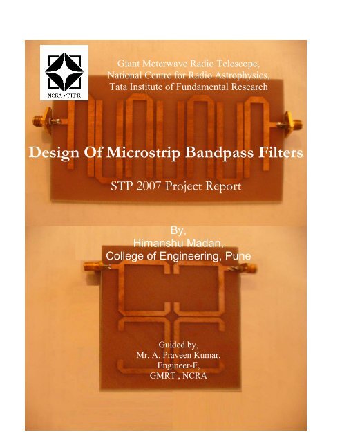
Giant Meterwave Radio Telescope,National Centre for Radio Astrophysics,<strong>Tata</strong> <strong>Institute</strong> <strong>of</strong> <strong>Fundamental</strong> Research<strong>Design</strong> <strong>Of</strong> <strong>Microstrip</strong> <strong>Bandpass</strong> <strong>Filters</strong>STP 2007 Project ReportBy,Himanshu Madan,College <strong>of</strong> Engineering, PuneGuided by,Mr. A. Praveen Kumar,Engineer-F,GMRT , NCRA1
AcknowledgementWorking at Giant Meterwave Radio Telescope for my summer project for a secondtime, has been a very enriching experience for me. I am very thankful to Mr. A. PraveenKumar, Engineer-F, GMRT, who has guided and supported me throughout my stint here.Technically as well as pr<strong>of</strong>essionally, I have gained a lot through my association withhim during my entire project work. I also would like to express my sincere gratitude toMr. Anil Raut for providing me with much needed guidance regarding the computationalcomponent <strong>of</strong> the project, which required intensive analysis using s<strong>of</strong>twares.I would also like to take this opportunity to thank Mr. Vilas Bhalero, whosesupport has been indispensable throughout and specially in developing the protoype filter.I express my sincere gratitude to Mr. G. Shankar and Mrs. Manisha Parate for theircooperation throughout my project stage.Gajenda Mulay and Santosh Bhor have been very helpful and cooperativeduring the project, many thanks to them. I also take this opportunity to thank my hostelinmates Avesh, Sandeep, Subhash, Sachin, Shelton, Raj and Shekher for all thosecolourful and memorable moments.Himanshu Madan
IndexContentspage no1. Introduction 12. Network Theory 22.1 Scattering Parameters 32.2 Open Circuit Impedance Parameters 42.3 Short-Circuit Admittance Parameters 42.4 ABCD parameters 52.5 Important Definition 62.5.1 Insertion Loss 62.5.2 Return Loss 62.5.3 Voltage Standing Wave Ratio 62.5.4 Phase Delay 62.5.5 Group Delay 72.6 Immittance Inverter 83. <strong>Microstrip</strong> Basics 113.1 Waves In <strong>Microstrip</strong> Line 113.2 Effective Dielectric Constant 123.3 Characteristic impedance 123.4 Some Other Formulae 133.4.1 W/h 133.4.2 Guided Wavelength 143.4.3 Propagation Constant 14III
3.4.4 Phase Velocity 143.4.5 Electrical Length 143.5 Effect <strong>of</strong> Metal Strip Thickness 143.6 Surface Waves And Higher-Order Modes 153.7 Coupled Lines 163.7.1 Even Mode 163.7.2 Odd Mode 173.8 Lumped Elements to <strong>Microstrip</strong> Transform 184. Hairpin Filter 214.1 Hairpin Resonator 214.2 Tapped line input 224.3 <strong>Design</strong> Parameter For Hairpin Filter 235. Open Loop, Cross coupled Planar Filter 255.1 Four pole Open Loop, Cross Coupled <strong>Bandpass</strong> Filter 265.2 <strong>Design</strong> Parameter for Four pole Open Loop, Cross 27Coupled <strong>Bandpass</strong> Filter6. Coupling <strong>of</strong> <strong>Microstrip</strong> Resonators 296.1 Coupling Coefficient 296.2 Electric Coupling 296.3 Magnetic Coupling 326.4 Magnetic Coupling 346.5 Coupling Coefficient Graph 377. Filter <strong>Design</strong> Using S<strong>of</strong>tware 397.1 Schematic <strong>of</strong> Filter 39IV
7.2 800-900 MHz <strong>Bandpass</strong> Filter <strong>Design</strong> 417.3 <strong>Design</strong> Procedure 417.4 Schematics 427.4.1 Hairpin Filter 427.4.2 Open Loop, Cross coupled Filter 437.5 Simulated Response 447.5.1 Hairpin Filter 447.5.2 Open Loop, Cross coupled Filter 458. Results 468.1 Layout 478.1.1 Hairpin Filter 478.1.2 Open Loop, Cross coupled Filter 488.2 Measured Response 498.2.1 Hairpin Filter 498.2.2 Open Loop, Cross coupled Filter 508.3 Comparison Table 519. References 5210. Appendix 54A. Filter Basics 54A.1 Pole zero concept 55A.2 Some Filter Response 55A.2.1 Butterworth Response 55A.2.2 Chebyshev Response 56A.2.3 Elliptical Function Response 58V
A.2.4 Bessel <strong>Filters</strong>(Maximally Flat Delay <strong>Filters</strong>) 59B. Result Plots 61B.1 Hairpin Filter 61B.1.1 Insertion Loss (S 21 in dB) 61B.1.2 Return Loss (S 11 in dB) 62B.1.3 SWR 63B.1.4 Group Delay 64B.1.5 Wide Band Response 65B.2 Open Loop, Cross Coupled Filter 66B.2.1 Insertion Loss (S 21 in dB) 66B.2.2 Return Loss (S 11 in dB) 67B.2.3 SWR 68B.2.4 Group Delay 69B.2.5 Wide Band Response 70VI
Chapter OneIntroductionMicrowave filters are vital components in a huge variety <strong>of</strong> electronic systems,including mobile radio, Satellite Communication Receivers and Radar. Due to theadvancement in the field <strong>of</strong> mobile and wireless communications, fully integratedanalogue filters for high-frequency applications are now receiving great interestworldwide.The use <strong>of</strong> microstrip in the design <strong>of</strong> microwave components and integratedcircuits has gained tremendous popularity since the last decade because microstrips canoperate in a wide range <strong>of</strong> frequencies. Furthermore, microstrip is lightweight, easy t<strong>of</strong>abricate and integrate in a cost effective way. Many researchers have presentednumerous equations for the analysis and synthesis <strong>of</strong> microstrips. But with advent <strong>of</strong>various Full Wave EM Simulators the designing <strong>of</strong> Microwave structures have becomeeasier.This project deals with the designing and fabrication <strong>of</strong> different types <strong>of</strong>microstrip bandpass filters. The designing is done using AWR Microwave <strong>Of</strong>ficesimulation program developed by Applied Wave Research USA. In the design <strong>of</strong> aMicrowave filter using microstrips two types <strong>of</strong> design approaches are taken. First,transforming the lumped element design to equivalent planar structure. Second, usingmicrostrip resonators and the concepts <strong>of</strong> immitance inverter. For the bandpass design thesecond approach is used.Two types <strong>of</strong> filter design are dealt in this project. Hairpin <strong>Bandpass</strong> filter andOpen Loop, Cross Coupled <strong>Bandpass</strong> filters. Hairpin filter has a Chebyshev responsewhere as the Open Loop, Cross Coupled filter gives a elliptical response. With the help <strong>of</strong>the elliptical response Open Loop, Cross Coupled filter achieves a sharper cut <strong>of</strong>f.1
Chapter TwoNetwork TheoryMost <strong>of</strong> the RF and Microwave systems and devices can be modeled as a two portnetwork. The two port representation basically helps in isolating either a complete circuitor a part <strong>of</strong> it and finding its characteristic parameters. Once this is done, the isolated part<strong>of</strong> the circuit, with a set <strong>of</strong> distinctive properties, enables us to abstract away its specificphysical buildup, thus simplifying analysis. Any circuit can be transformed into a twoportnetwork provided that it does not contain an independent source.Z o2 a 1V 2E s~b 1Two-PortV 1Networkb 2a 2Z o2Figure 2.1: Two port network with its wave variablesWhere V 1 , V 2 and I 1 , I 2 are the voltages and currents at respective ports and Z o1and Z o2 are the terminal impedances. At RF and Microwave frequencies it is difficult tomeasure the voltages, thus new wave variables a 1 , b 1 and a 2 , b 2 are introduced with asignifying the incident wave and b implying the reflected wave.The wave variables in terms <strong>of</strong> voltage and current are defined as followsnon( a b )V = Z +nnIn=1Zon( a − b )nnfor n=1 and 2oran1 ⎛⎜Vn= + ZonIn2⎝ Zon⎞⎟⎠2
n1 ⎛⎞⎜Vn= − Z ⎟onIn2 ⎜⎟⎝ Zon ⎠for n=1 and 2Which gives power at each port P n* 1 * *( V ⋅ I ) = ( a a − b b )1Pn= Ren nn n n n22Now we will see few types <strong>of</strong> parameters used to define a two port network2.1 Scattering ParametersThese are a set <strong>of</strong> parameters describing the scattering and reflection <strong>of</strong> travelingwaves when a network is inserted into a transmission line. S- parameters are normallyused to characterize high frequency networks, where simple models valid at lowerfrequencies cannot be applied. S-parameters are normally measured as a function <strong>of</strong>frequency, so when looking at the formulae for S-parameters it is important to note thatfrequency is implied, and that the complex gain (i.e. gain and phase) is also assumed. Forthis reason, S-parameters are <strong>of</strong>ten called complex scattering parameters.S11=ba11a2 = 0S12=ba12a1=0S21b=a21a2 = 0S22=ba22a1 = 0S11is the reflection coefficient <strong>of</strong> the inputS22is the reflection coefficient <strong>of</strong> the outputS21is the forward transmission gainS12is the reverse transmission gainThese definitions can also be written in a matrix form as⎡b⎢⎣b12⎤ ⎡S⎥ = ⎢⎦ ⎣S1121SS1222⎤ ⎡⎥ ⋅ a⎢⎦ ⎣a12⎤⎥⎦3
2.2 Open Circuit Impedance ParametersImpedance parameters are very useful in designing impedance matching andpower distribution systems. Two port networks can either be voltage or current driven.For the current driven networks the input and output terminal voltage can be presented inmatrix form as follows:⎡V⎢⎣V12⎤ ⎡Z⎥ = ⎢⎦ ⎣Z1121ZZ2122⎤ ⎡⎥ ⋅ I⎢⎦ ⎣IWhere the matrix which contain the z parameter is also called z matrix and is denoted by[z]12⎤⎥⎦The z parameters for a two port network can be mathematically defined asZ11V=I11I2 = 0Z12V=I12I1=0Z21V=I21I2 = 0Z22V=I22I1 = 0For reciprocal network Z12= Z 21. For a symmetrical network Z12= Z21andZ11= Z 22. And for lossless network, the z parameters are imaginary.2.3 Short-Circuit Admittance ParametersAdmittance parameters are very useful for describing the network when impedanceparameters may not be existing. This is solved by finding the second set <strong>of</strong> parameters byexpressing the terminal current in terms <strong>of</strong> the voltage. The input and output terminalcurrent can be presented in matrix form as follows:⎡I⎢⎣I12⎤ ⎡Y⎥ = ⎢⎦ ⎣Y1121YY1222⎤ ⎡⎥ ⋅ V⎢⎦ ⎣V12Where the matrix which contain the y parameter is also called y matrix and is denoted by[y]⎤⎥⎦4
The Y parameters for a two port network can be mathematically defined asY11I=V11V2 = 0Y12I=V12V1 = 0Y21I=V21V2 = 0Y22I=V22V1=0Y11= Y 22For reciprocal network Y12= Y21. For a symmetrical network Y12= Y 21and. And for lossless network, the y parameters are imaginary.2.4 ABCD parametersIn ABCD parameter the input port voltage and current are considered variable andequation is formed in terms <strong>of</strong> the output voltage and current. The equation can berepresented in matrix form as follows:⎡V1⎤ ⎡A⎢ ⎥ = ⎢⎣I1⎦ ⎣CB⎤⎡⎥ ⋅ V2D⎢⎦ ⎣−I2⎤⎥⎦The ABCD parameters for a two port network can be mathematically defined asVA =V12I2 = 0B =V1−I2V2 = 0IC =V12I2 = 0D =I1−I2V2 = 0AD-BC=1 for reciprocal networkAnd A=D for symmetrical networkABCD parameters are useful in analysis when the network can be broken into cascadedsub networks.5
2.5 Important Definition2.5.1 Insertion LossThe loss resulting from the insertion <strong>of</strong> a network in a transmission line,expressed as the reciprocal <strong>of</strong> the ratio <strong>of</strong> the signal power delivered to that part <strong>of</strong> theline following the network to the signal power delivered to that same part beforeinsertion. It is usually expressed in dB.L= −20logdB m, n = 1, 2 ( m ≠ n)AS mnwhere L A denotes the insertion loss between the ports n and m.2.5.2 Return LossThe Return Loss <strong>of</strong> a line is the ratio <strong>of</strong> the power reflected back from the line tothe power transmitted into the line. It is usually expressed in dB.L= 20logdB n = 1, 2RS nn2.5.3 Voltage Standing Wave RatioA standing wave may be formed when a wave is transmitted into one end <strong>of</strong> atransmission line and is reflected from the other end by an impedance mismatch. VSWRis the ratio <strong>of</strong> the maximum to minimum voltage in a standing wave pattern.VSWR1+= 1 −SSnnnnn = 1,2.2.5.4 Phase DelayWhenever we insert a sinusoid into a filter, a sinusoid must come out. The onlything that can change between input and output are the amplitude and the phase.Comparing a zero crossing <strong>of</strong> the input to a zero crossing <strong>of</strong> the output measures the so-6
called phase delay. To quantify this we define an input, sin( ωt)and an output ( ωt−φ)Then the phase delay τpis found by solvingsin( ωt− φ)= sinωωt− φ = ωt− ωτ( t −τ)φτp= secondsωppsin .Where φ is in radians and ω is in radians per second. The phase delay is actually thetime delay for a steady sinusoidal signal and is not necessarily the true signal delaybecause a steady sinusoidal signal doesn’t carry information.2.5.5 Group Delay<strong>Of</strong>ten the group delay is nothing more than the phase delay. This happens whenthe phase delay is independent <strong>of</strong> frequency. But when the phase delay depends onfrequency, then a completely new velocity, the “group velocity" appears. Curiously, thegroup velocity is not an average <strong>of</strong> phase velocities.The simplest analysis <strong>of</strong> group delay begins by defining a filter input x t as the sum<strong>of</strong> two frequencies:x t 2= cosω 1t + cosωtBy using a trigonometric identity,x ⎛ ω1 − ω2⎞ ⎛ ω1+ ω2⎞= 2cos⎜t ⎟cos⎜t ⎟t⎝ 2 ⎠ ⎝ 2 ⎠We see that the sum <strong>of</strong> two cosines looks like a cosine <strong>of</strong> the average frequencymultiplied by a cosine <strong>of</strong> half the difference frequency.Each <strong>of</strong> the two frequencies could be delayed a different amount by a filter, sotake the output <strong>of</strong> the filter y t to be7
y t( ω t − φ ) + ( ω −φ)= cost1 1cos22In doing this, we have assumed that neither frequency was attenuated. (The groupvelocity concept loses its simplicity and much <strong>of</strong> its utility in dissipative media.) Usingthe same trigonometric identity, we find thaty t⎛ ω − ω2φ1−φ2⎞ ⎛ ω1+ ω2φ1+= 2cos⎜t − ⎟cos⎜t −⎝ 2 2 ⎠ ⎝ 2 21φ2⎞⎟⎠Rewriting the beat factor in terms <strong>of</strong> a time delay t g , we now have⎡ω− ω2cos⎢⎣ 2⎤ ⎛ ω1− ω2φ1−2 ⎞( − t ) = cos⎜t − ⎟⎠1φtg⎥⎦( ω1 − ω2) tg= φ1− φ2⎝22tgφ1− φ2=ω − ω12=ΔφΔωFor a continuum <strong>of</strong> frequencies, the group delay isdφt g=dωThis represents the true signal (baseband signal) delay, and is also referred to as theenvelope delay.2.6 Immittance InverterImmittance Inverters are <strong>of</strong> two types, Impedance Inverter and Admittanceinverter. The following Block diagram shows a Immittance Inverter.8
Admittance/ImpedanceInverterY 1orZ1Y2orZ 2Figure 2.2: Immittance InverterAn ideal Impedance Inverter is a two-port network that has a unique property atall frequencies, i.e. if it is terminated in impedance Z 1 on one port, the impedance Z 2 seenlooking in the other port isZ =2KZ21where K is real and defined as characteristic impedance <strong>of</strong> the inverter. Animpedance inverter converts a capacitance to inductance and vice versa. The ABCDmatrix <strong>of</strong> the impedance inverter is⎡A⎢⎣C⎡ 0B⎤= ⎢⎥1D⎦⎢±⎣ jKm jK ⎤⎥0 ⎥⎦Similarly an ideal Admittance Inverter is a two-port network that if terminated inadmittance Y 1 on one port, the impedance Y 2 seen looking in the other port isY =2JY21where J is real and defined as characteristic admittance <strong>of</strong> the inverter. Likewisean admittance inverter converts a capacitance to inductance and vice versa. The ABCDmatrix <strong>of</strong> the admittance inverter is⎡ 1 ⎤⎡AB⎤⎢0 ±=⎥⎢ ⎥jJ⎣CD⎦⎢ ⎥⎣mjJ 0 ⎦9
Properties <strong>of</strong> Immitance InverterIf a series inductance is present between two Impedance Inverters, it looks like ashunt capacitance from its exterior terminals.KLKCFigure 2.3: Immitance inverter used to convert a shunt capacitance into a equivalentcircuit with series inductance.Similarly if a shunt capacitance is present between two Admittance Inverters, itlooks like a series inductance from its exterior terminals.LJJCFigure 2.4: Immitance inverter used to convert a series inductance into a equivalentcircuit with shunt capacitance.Making use <strong>of</strong> the properties <strong>of</strong> Immittance Inverters, bandpass filters may berealized by series LC. resonant circuits separated by Impedance Inverters (K) or shuntLC. parallel resonant circuits separated by Admittance Inverters (J).10
Chapter Three<strong>Microstrip</strong> BasicsA general microstrip structure is shown in the figure 3.1, a microstip transmissionline consists <strong>of</strong> a thin conductor strip over a dielectric substrate along with a ground plateat the bottom <strong>of</strong> the dielectric.WtConducting stripGround plateε rDielectric substratehFigure 3.1: A basic <strong>Microstrip</strong> structure3.1 Waves In <strong>Microstrip</strong> LineWave traveling in microstip line not only travel in the dielectric medium they alsotravel in the air media above the microstrip line. Thus they don’t support pure TEMwaves. In pure TEM transmission, the waves have only transverse component and thepropagation velocity only depends on the permittivity and the permeability <strong>of</strong> thesubstrate. But in the case <strong>of</strong> microstrip line the magnetic and electric field also contain alongitudinal component, and their propagation velocity is dependent on the physicaldimensions <strong>of</strong> the <strong>Microstrip</strong> as well.If this longitudinal component is much smaller than the transverse componentthen the microstrip line can be approximated to TEM model. And this is called quasiTEM approximation.11
3.2 Effective Dielectric ConstantDue to presence <strong>of</strong> two dielectric medium, air and the substrate, the effectivedielectric constant replaces the relative dielectric constant <strong>of</strong> the substrate in the quasiTEM approximation. This effective dielectric constant is given in terms <strong>of</strong> C d,capacitance per unit length with the dielectric substrate present and C a , capacitance perunit length with dielectric constant replaced by air and is given byεreC=CdaThe effective dielectric constant in terms <strong>of</strong> W (width <strong>of</strong> the <strong>Microstrip</strong>), h (height<strong>of</strong> the substrate) and εr(relative dielectric constant) given by Hammerstad and Jensen[5]is:whereεreεr+ 1 εr−1⎛ 10 ⎞= + ⎜1+ ⎟2 2 ⎝ u ⎠Wu = , andha = 1+1ln49⎡⎢u⎢⎢ u⎢⎣0 ⎛ εr− 0.9.5643 ⎟ ⎞b =⎜⎝ εr+ ⎠42⎛ u ⎞ ⎤+ ⎜ ⎟ ⎥⎝ 52 ⎠ ⎥ ++ 0.432 ⎥⎥⎦40.053−ab118.7⎡ ⎛ u ⎞ln⎢1+ ⎜ ⎟⎢⎣⎝18.1⎠Accuracy <strong>of</strong> this model is 0.2% forε ≤ 128 and 0.01≤ u ≤ 100r3⎤⎥⎥⎦3.3 Characteristic impedanceCharacteristic impedance <strong>of</strong> the microstrip line is given byZc=c1CaCd8where c is the velocity <strong>of</strong> electromagnetic waves in free space c = 2.99×10 m / s .12
Expression for characteristic impedance by hammerstad and Jensen[5] iswhereZcη ⎡F⎢⎛ 2 ⎞= ln + 1+⎜ ⎟2πε ⎢ u⎣⎝ ure⎠Wu = , η = 120πohms (free space impedance), andh2⎤⎥⎥⎦⎡ ⎛ 30.666 ⎞F = 6 + (2π− 6)exp⎢−⎜ ⎟⎢⎣⎝ u ⎠0.7528⎤⎥⎥⎦The accuracy <strong>of</strong>Z ε is better than 0.01% for u ≤ 1 and 0.03% for u ≤ 1000cre3.4 Some Other Formulae3.4.1 W/hFor W/h ≤ 2withWh8exp( A)=exp(2A)− 2for W/h ≥ 2A =0.5Z c ⎧ εr+ 1⎫εr−1⎧ 0. 11⎫⎨ ⎬ + ⎨0.23+ ⎬60 ⎩ 2 ⎭ εr+ 1 ⎩ εr ⎭withWh2 ⎧= ⎨π ⎩ε −1⎡⎢2εr ⎣r( B −1) − ln( 2B−1) + ln( B −1)0.61⎤⎫+ 0.39 − ⎥⎬εr ⎦⎭B =60π 2Z cεr13
3.4.2 Guided Wavelength=λ0λgεrewhere λ0is the free space wavelength at frequency f.3.4.3 Propagation Constant2πβ =λ g3.4.4 Phase Velocityvpω = =βcεre3.4.5 Electrical LengthThus,θ = βlθ is called the electrical length whereas l is the physical length <strong>of</strong> the microstrip.πθ = when2λgλgl = and θ = π when l = . These are called quarter wavelength42and half wavelength microstrip line and are important in the filter design.3.5 Effect <strong>of</strong> metal strip thicknessWhen the strip thickness t becomes comparable to the width <strong>of</strong> the substrate thenits effect needs to be considered while designing. The following formulae show its effecton the characteristic impedance and effective dielectric constant.14
For W/h ≤ 1For W/h ≥ 1Z ( t)=c2πηεre⎡ln⎢⎣We8 We( t)⎤+ 0.25 ⎥( t) / h h ⎦whereZ ( t)=cη ⎡We( t)⎛We( t)⎞⎤⎢ + 1.393 + 0.667 ln⎜+ 1.444⎟⎥ε ⎣ h⎝ h ⎠⎦re−1⎧W1.25 t ⎛ 4πW⎞⎪ + ⎜1+ ln ⎟W e( t)h π h ⎝ t ⎠= ⎨h ⎪W1.25 t ⎛ 2h⎞+ ⎜1+ ln ⎟⎪⎩h π h ⎝ t ⎠WhWh≤ 0.5π≥ 0.5πε ( t)= εrereεre−1−4.6t / hW / hwhere εreis the effective dielectric constant with t=0. It can be seen from theformulae that the effect <strong>of</strong> t is insignificant for small values <strong>of</strong> t/h ratio.3.6 Surface Waves And Higher-Order ModesDespite the absence <strong>of</strong> the top conductor there exists wave on ground plate guidedby the air dielectric medium. These are called surface waves. The frequency at whichthese become significantly large isfs=−c tan 1 ε2πhε −1rrwhere the phase velocity <strong>of</strong> the two modes become equal.To avoid excitation <strong>of</strong> higher-order modes in <strong>Microstrip</strong> the frequency <strong>of</strong>operation is kept below the cut <strong>of</strong>f frequencyfcrc( 2 W + 0.8h)=ε15
3.7 Coupled LinesThe following figure shows the cross section <strong>of</strong> a coupled line. Widely used in theconstruction <strong>of</strong> filters, they support two modes <strong>of</strong> excitation, even and odd mode.W s WεrtFigure 3.2: A Coupled Line Structure.3.7.1 Even ModeIn even mode excitation both the microstrip coupled lines have the same voltagepotential resulting in a magnetic wall at the symmetry plane.Magnetic wall+ + + + + + + +C fC pC’ fC’ fC pC fFigure 3.3: Quasi-TEM, Even Mode <strong>of</strong> a Pair <strong>of</strong> Coupled <strong>Microstrip</strong> LinesEven mode capacitance is given byC = C + C + Cepf'fwhereC pis the parallel plate capacitance between the microstrip line and the groundplate. HenceCp=ε 0Wεrh16
Cfis the fringe capacitance and is given by2 Cf= εcZrec− CpAnd'C fis the modified fringe capacitance, with the effect <strong>of</strong> the adjacentmicrostrip included.whereC'fCf=1+A(h / s) tanh(8s/ h)[ − 0.1exp( 2.33 − 2. )]A = exp53 W hThe even mode characteristic impedance can also be obtained from thecapacitanceZce= ( cC Ceae)−1whereaC eis the even mode capacitance with air as a dielectricAnd the effective dielectric constant for even mode is given as :εereC=Ceae3.7.2 Odd ModeIn odd mode the coupled microstrip line possess opposite potential. This resultsinto a electric wall at the symmetry. The following cross section diagram shows the same.Electric wallC gaC ga+ + + + − − − −C fC pC gdC gdC pC fFigure 3.4: Quasi-TEM, Odd Mode <strong>of</strong> a Pair <strong>of</strong> Coupled <strong>Microstrip</strong> Lines17
The resulting odd mode capacitance is given asgaC = C + C + C + CopfgdgaC and represent fringe capacitance between the two microstrip line overC gdthe air and over the dielectric.whereCgak =k'=K= εoKsh'( k )( k)sh+ 2 Wh1−k( k )And the ratio <strong>of</strong> the elliptic functionKK'( k )( k)2⎧ 1 ⎛⎪ ⎜ 1+kln 2⎪π⎜⎝ 1−k⎪= ⎨ π⎪⎪ ⎛ 1+k ⎞ln⎜⎟⎪2⎩ ⎝ 1−k ⎠K ' is given byK''( k)⎞⎟⎟⎠for0≤ k2for0.5≤ k≤ 0.5The odd mode characteristic impedance and effective dielectric constant is given as:2≤ 1Zco= ( cCoCao)−1whereaC eis the even mode capacitance with air as a dielectric.εoreC=Coao3.8 Lumped Elements to <strong>Microstrip</strong> TransformThe following figure shows a simple LC low pass filter circuit. At microwavefrequencies the <strong>Microstrip</strong> lines act as inductor and capacitor. The <strong>Microstrip</strong> line has18
oth capacitance and inductance. If the <strong>Microstrip</strong> lines are made wide they have morecapacitance and lower inductance and vice versa.L 1 L 2 L 3Z 0 Z 0C 1 C 2Figure 3.5: Lumped Element LC Lowpass Filter.The following figure shows the equivalent microstrip realization <strong>of</strong> the lumpedelement filter.l LZo≈ C 1≈ C2Zo≈ L 1≈ L2≈ L3Figure 3.6: <strong>Microstrip</strong> Realization <strong>of</strong> a Lowpass Filter.l CThe important consideration while transforming isZ0 CZ0< Z0L< , where Z 0Cand Z 0L denote the characteristic impedances <strong>of</strong> the low and high impedance lines,respectively, and Z 0 is the source impedance, which is usually 50 ohms for microstripfilters.A lower Z 0C , results in a better approximation <strong>of</strong> a lumped-element capacitor, butthe resulting line width W, must not allow any transverse resonance to occur at operatingfrequencies.A higher Z 0L , leads to a better approximation <strong>of</strong> a lumped-element inductor, butZ 0L must not be so high that its fabrication becomes inordinately difficult as a narrowline, or its current-carrying capability becomes a limitation.19
The length <strong>of</strong> the capacitive and inductive microstrip lines can be calculated fromthe following equationslLλgL= sin2πλ−1⎛ ωcL ⎞⎜⎟⎝ Z0L⎠( ω CZ )gC −1lC= sinc 0C2πwhere λgLand λgCare the guided wavelength <strong>of</strong> the inductive and capacitivemicrostrip line respectively and ωcis the frequency <strong>of</strong> operation in radians. which isusually 50 ohms for microstrip filters. Although the above formulae takes into accountthe capacitive effect <strong>of</strong> the low-impedance line and the inductive effect <strong>of</strong> the highimpedance line but it does not take into account the series reactance <strong>of</strong> the lowimpedanceline and the shunt susceptance <strong>of</strong> the high-impedance lines. To include theseeffects, the lengths <strong>of</strong> the high and low impedance lines should be adjusted to satisfy thefollowing equations.ω L = Zc0 L⎛ ⎞⎜2πlLsin ⎟ + Z0⎝ λgL⎠C⎛⎜πltan⎝ λCgC⎞⎟⎠ω C =c1Z0C⎛⎜2πlsin⎝ λgCC⎞⎟1+ 2×⎠ Z0L⎛⎜πltan⎝ λLgL⎞⎟⎠20
Chapter fourHairpin FilterOut <strong>of</strong> various bandpass microstrip filters, Hairpin filter is one <strong>of</strong> the mostpreferred one. The concept <strong>of</strong> hairpin filter is same as parallel coupled half wavelengthresonator filters.The advantage <strong>of</strong> hairpin filter over end coupled and parallel coupled microstriprealizations, is the optimal space utilization. This space utilization is achieved by folding<strong>of</strong> the half wavelength long resonators. Also the absence <strong>of</strong> any via to ground plane orany lumped element makes the design simpler. The following figure shows a typicalhairpin structure.(a)(b)Figure 4.1: (a) tapped line input 5-pole Hairpin Filter (b) coupled line input 5-poleHairpin Filter4.1 Hairpin ResonatorFigure 4.2 shows a single Hairpin Resonator. α is called theslide angle. If the slide angle is small it might lead to coupling betweenthe arms <strong>of</strong> individual resonator. The voltage at the end <strong>of</strong> hairpin armsis antiphase, and thus causes the arm to arm capacitance to have λ4seemingly disproportionate effect. The added capacitance lowers theresonant frequency requiring a shortening <strong>of</strong> the hairpin to compensate.αTo avoid this, slide angle is kept as large as possible. ButFigure 4.2: Hairpin Resonatorby increasing the slide angle the coupling length between tworesonators reduces, so as to attain the required coupling, the coupling spacing needs to be21
educed which posses a practical limitation. For practical design purpose slide angle iskept twice the strip width to avoid inter-element coupling.4.2 Tapped line inputConventional filters employ coupled line input. Tapped line input has a spacesaving advantage over coupled line input. Further while designing sometime the couplingdimensions required for the input and output coupled line is very small and practicallynot achievable which hinders the realizability <strong>of</strong> the design. Thus tapped line input ispreferred over coupled line input.L = π 2πZ o2θ = πθ1ltap = θ 1Y(a)(b)Figure 4.3: (a) Tapped Hairpin Resonator Schematic. (b) Equialent Circuit <strong>of</strong> a TappedHairpin ResonatorAssuming negligible coupling between the arms <strong>of</strong> the hairpin resonator, the inputadmittance at the tap point can be given asY= G +πY⎛01 f − fjB =⎜ + j222sinθ1⎝ Qef00⎞⎟⎠provided thatf−f0f0
And⎡⎢⎣θ( f − f )f00⎤⎥ cotθ1
Coupling coefficient and Quality Factor can be calculated asgg0 1Q e 1=Qen=FBWgngn+1FBWFBWMi,i+ 1=for i = 1 to n-1g gii+1where FBW is the fractional bandwidth andg0 ,1...... n+1are the normalized lowpass element<strong>of</strong> the desired low pass filter approximation.The quality factor can be substituted and the ltap length can be calculated as⎛ Z2L⎜−1πltap = sin ⎜π ⎜ 2⎝λg o2 L = = =22λεre0Q e2 f⎞⎟R⎟⎟⎠0Cεre24
Chapter FiveOpen Loop, Cross coupled Planar FilterWhen the frequency selectivity and low band pass loss are considered to be theprime importance then elliptical filters are employed. Elliptical filters exhibit equi-rippleresponse in both passband and stopband.Simple concept <strong>of</strong> multipath propagation is used to cancel out signals and toobtain transmission zero at finite frequency or group delay flattening or bothsimultaneously. Although such multipath filters are realized using waveguide cavities ordielectric resonator loaded cavities, because <strong>of</strong> their low insertion loss can also bedeveloped as planar structure. This is achieved by employing cross coupling between twononadjacent resonator.(a)(b)(c)Figure 5.1: (a) Four Pole (b) Six Pole (c) Eight Pole cross coupled planar microwavebandpass filters.25
5.1 Four pole Open Loop, Cross Coupled <strong>Bandpass</strong> FilterThe low pass prototype <strong>of</strong> the filter can be seen in the figure below. The crosscoupling can be seen with the admittance inverter J 1. The value <strong>of</strong> J1 decides the location<strong>of</strong> transmission zero.g 0g 1J=1g 2J J12g 0g 1J=1g 2Figure 5.2: Lowpass Prototype <strong>of</strong> Four pole Open Loop, Cross Coupled Filter.The value <strong>of</strong> low pass prototype component can be calculated from the followingformulae as described in [].gg1=2g1π2sin2nγ3π14sin sin=8 82 2 πγ + sin4⎛ 1γ = sinh⎜sinh⎝ 4−1( 1+ ε ) 2 + ε21 ⎞⎟ε ⎠S =(the passband VSWR)For Chebyshev response the cross coupling can be eliminated and thus theadmittance inverters become:J = 0 126
J2=1SFor elliptical filter in order to introduce a transmission zero at ω = ±ωa, the requiredvalue <strong>of</strong> J 1 is given byJ1=ω− J( g )and the modified J2a22'2− J' 22J'2J2=1+J J215.2 <strong>Design</strong> Parameter for Four pole Open Loop, Cross Coupled <strong>Bandpass</strong> FilterThe low pass filter prototype can be converted to the required bandpass filterdesign. The equivalent circuit diagram for the planar filter is given below. M 12, M 23 andM 34 are the mutual coupling coefficient between the adjacent resonators. The M 14 is themutual coupling coefficient between the nonadjacent resonator 1 and 4.M 14C C C Ci/pL/2 L/2 L/2 L/2 L/2 L/2 L/2 L/2Q eM 12M 23 M 34Q eFigure: Equivalent circuit <strong>of</strong> the Four pole Open Loop, Cross Coupled <strong>Bandpass</strong> Filter.27
g0g=FBWQ e1M = M =1234FBWg g12MM2314==FBW ⋅ Jg2FBW ⋅ Jg121where FBW is the fractional bandwidth.28
Chapter SixCoupling <strong>of</strong> <strong>Microstrip</strong> ResonatorsCoupling <strong>of</strong> two resonators is the primary component <strong>of</strong> a bandpass filter design.Coupling between two resonators is basically due to the fringe fields. The nature and theextent <strong>of</strong> these fringes determine the strength and thtype <strong>of</strong> coupling. There are threetypes <strong>of</strong> basic coupling, electric coupling, magnetic coupling and mixed couplinginvolving both electric and magnetic coupling. In the subsequent sections we will analyzesquare open loop resonators for various coupling properties.6.1 Coupling CoefficientCoupling coefficient is a dimensionless quantity. It is defined as the ratio <strong>of</strong>coupled energy to stored energy in the resonator. It can be mathematically given askeCm= electric coupling coefficientCwhere C m is the mutual capacitance between the two resonator and C is the selfcapacitance <strong>of</strong> the resonatorLmkm= magnetic coupling coefficientLwhere L m is the mutual inductance between the two resonator and L is the selfinductance <strong>of</strong> the resonator6.2 Electric CouplingAt resonance, the open loop resonator has the maximum electric field density atthe side with an open gap. This is because the fringe field at the open end is the strongest.Thus an electric coupling can be achieved by having the sides with open gap proximatelyplaced. Thus the planar structure shown in the figure exhibit electric coupling.29
Figure 6.1: Electric Coupling StructureThe equivalent circuit <strong>of</strong> the planar structure can be drawn asT 1 T 2C mI 1 I 2LV 1 1 C V 2T ’ 1 T ’ 2Figure 6.2: Equivalent circuit diagram <strong>of</strong> the coupled open-loop resonator exhibitingelectric couplingThe C and L are the self capacitance and self inductance <strong>of</strong> the uncoupledresonator and C m represents the mutual capacitance. The angular resonant frequency <strong>of</strong>the uncoupled resonator is given by1LC.If the network from reference plane T 1 -T ‘ 1 to T -T ‘2 2 is considered, then we can seea two port network. The following equations describe the networkII=ω−ω1j CV1j CmV2=ω−ω2j CV2j CmV1The second term in the equations corresponds to the current induced by theadjacent resonator. Thus the Y parameters <strong>of</strong> the network can be given as30
⎡Y⎢⎣Y1121YY1222⎤ ⎡ jωC⎥ = ⎢⎦ ⎣−jωCm−jωCjωCAlternative form <strong>of</strong> the network can be drawn with an admittance inverterJ = ωC min between the two resonant networks. The resulting equivalent network isshown in the figure.T 1 TT 22C m 2C mI 1 I 2m⎥ ⎦⎤LLV 1 C-C m -C mC V 2T ’T ’ 1 T ’ 2J = ωC mFigure 6.3: Equivalent circuit with admittance inverterJ = ωC mto represent the couplingIf this equivalent circuit is short circuit at the plane <strong>of</strong> symmetry T-T ’ , i.e. anelectric wall is introduced at the plane T-T ’ , then due to the effect <strong>of</strong> the adjacentresonator the capability <strong>of</strong> storing charge <strong>of</strong> the single resonator is enhanced. This resultsin a resonant frequency lower than that <strong>of</strong> the uncoupled resonator.fe=2 π1L(C + Cm)Similarly when a magnetic wall, i.e. a open circuit, inserted at the plane <strong>of</strong>symmetry T-T ’ , the coupling effect reduces the capability <strong>of</strong> storing charge. This resultsin the increased resonant frequency.fm21L(C − Cm)=π31
The electric coupling coefficient for the resonant network in terms <strong>of</strong> themagnetic and electric resonant frequency can be given askf−2 2m ee= =2 2fm+ fefCmCk e6.3 Magnetic CouplingAs stated earlier that at resonance the fringe field at the open end is the strongestwhich results in maximum electric field density at the side with an open gap. The fringefield exhibits an exponentially decaying character outside the region, thus the oppositeside to the open end has the maximum fringe field resulting into maximum magnetic fielddistribution. Thus to achieve magnetic coupling the sides with maximum magnetic fieldare proximately placed.Figure 6.4: Magnetic Coupling StructureThe equivalent circuit <strong>of</strong> the planar structure can be drawn asT 1 T 2L mCCV 1 V 2LLI 1 I 232T ’ 1 T ’ 2Figure 6.5: Equivalent circuit diagram <strong>of</strong> the coupled open-loop resonator exhibitingmagnetic coupling.
The C and L are the self capacitance and self inductance <strong>of</strong> the uncoupledresonator and L m represents the mutual capacitance. The angular resonant frequency <strong>of</strong>the uncoupled resonator is given by1LCSimilarly for this network we can see a two port network. The followingequations describe the networkVV=ω +ω1j LI1j LmI2=ω +ω2j LI2j LmI1The second term in the equations corresponds to the voltage induced by theadjacent resonator. Thus the Z parameters <strong>of</strong> the network can be given as⎡Z⎢⎣Z1121ZZ1222⎤⎥⎦⎡= ⎢⎣jωLjωLm.jωLm⎤jωL⎥⎦Alternative form <strong>of</strong> the network can be drawn with an impedance inverterK = ωL min between the two resonant networks. The resulting equivalent network isshown in the figure.T 1 TT 2I-L m - L m1 I 2CLLLC2L m 2L mV 1 CV 2T ’T ’ 1K = ωC mT ’ 2Figure 6.6: Equivalent circuit with impedance inverterK = ωLmto represent the coupling33
If an electric wall is introduced at the plane T-T ’ , then due to the effect <strong>of</strong> theadjacent resonator the flux in single resonator is reduced. This results in a resonantfrequency higher than that <strong>of</strong> the uncoupled resonator.fe1=2 π ( L − Lm) CSimilarly when a magnetic wall is inserted at the plane <strong>of</strong> symmetry T-T ’ , thecoupling effect increases the stored flux. This results in the resonant frequency lower thanthat <strong>of</strong> uncoupled resonator.fm1=2 π ( L + Lm) CThe magnetic coupling coefficientk mfor the resonant network in terms <strong>of</strong> themagnetic and electric resonant frequency can be given askf−2 2e mm= =2 2fe+ fmfLmL6.4 Mixed CouplingCases when the electric and magnetic field distribution <strong>of</strong> the coupled resonatorarms are comparable then neither the magnetic coupling nor the electric coupling can beignored. This type <strong>of</strong> coupling is called as Mixed Coupling. The following planarstructure exhibit Mixed Coupling.Figure 6.7: Mixed Coupling Structure34
This planar structure can be redrawn with impedance and admittance network parameter.-2Y 12 -2Y 12T 1 TT 2Z 11 -Z 12 Z 22 -Z 12Y 11 +Y 12 2Z 12 2Z 12Y 12 +Y 22T ’ 1 T ’T ’ 2Figure 6.8: Network representation <strong>of</strong> the open loop resonators exhibiting mixed couplingThe Y network Parameter can be given as⎡Y⎢⎣Y1121YY1222⎤⎥⎦⎡= ⎢⎣jωCjωC'mjωC'mjωC⎤⎥⎦And the Z parameter can be given as⎡Z⎢⎣Z1121ZZ1222⎤⎥⎦⎡= ⎢⎣jωL'jωLm'jωL⎤m⎥jωL⎦Where L and C are the self inductance and self capacitance <strong>of</strong> the individualresonators. And L ’ m and C ’ m are the mutual inductance and mutual capacitance.The network can also be drawn using the impedance inverterand admittance'inverter J = ωC m, which represent magnetic coupling and the electric coupling. Figure6.9is the equivalent circuit.'K = ωL m35
-2C ’ mT-2C ’ mC ’ mT 1T 2C ’ mCC'J = ωC mL-L ’ m - L ’ mLT ’ 12L ’ m2L ’ mT ’ 2T ’'K = ωL m'Figure 6.9: Equivalent circuit <strong>of</strong> mixed coupling with an impedance inverter k = ωL m'and an admittance inverter J = ωC mrepresenting the magnetic and electriccoupling respectively.Again by introducing an electric wall and a magnetic wall at the plane <strong>of</strong>symmetry T-T ’ one can obtain the electric and magnetic resonant frequency.ffe1=2 π''( L − Lm)( C − Cm)12'( L + L')( C + C )m=πm m36
So the resulting mixed coupling coefficient can be given bykB=ff2e2e−+ff2m2m'CLm+ LC=LC + L C'm'm'mWhen' 'Lm Cm
In the simulated plot one can see two peaks. These correspond to the electric andthe magnetic resonance for the resonator and the corresponding coupling coefficient canbe calculated. By varying the coupling space with the tuner, various values <strong>of</strong> resonantfrequency can be taken and the respective coupling coefficient can be calculated. Theseare then plotted on a graph to obtain the coupling coefficient curve.(a)(b)Figure 6.11: (a) Pair <strong>of</strong> Hairpin Resonator (b) Coupling Coefficient Curve.38
Chapter SevenFilter <strong>Design</strong> Using S<strong>of</strong>twareToday’s Microwave Engineer rely on advanced simulation s<strong>of</strong>tware’s andelectromagnetic analysis tools to develop and analyze microwave circuits. Using theseemulators benefit the designer by saving the time for repeated design and testing phaseand give the good approximation <strong>of</strong> the expected results.For the design <strong>of</strong> the bandpass filter, the design procedure using the AWRMicrowave <strong>Of</strong>fice simulation program developed by Applied Wave Research USA willbe described in this section.7.1 Schematic <strong>of</strong> FilterThe individual hairpin resonators can be modeled using the numerical modelsdeveoped by AWR.Figure 7.1: Section <strong>of</strong> Schematic in AWR Microwave <strong>Of</strong>fice39
The mopen(Open Circuit With End Effect (Closed Form)) model takes intoaccount the fringing effect <strong>of</strong> the conductor. The mline element models a length <strong>of</strong><strong>Microstrip</strong> Transmission Line. The model assumes a Quasi-TEM mode <strong>of</strong> propagationand incorporates the effects <strong>of</strong> dielectric and conductive losses. M2clin is advancednumerical model representing two edge coupled line. The distance between the bends <strong>of</strong>an individual resonator is kept more than twice the width <strong>of</strong> the microstrip conductor.To calculate the approx length <strong>of</strong> each hairpin resonator the TXline calculator <strong>of</strong>MWO is used.The dielectric used for this design is FR4. Its specifications are:Substrate thickness: 1.6mmRelative dielectric constant: 4.4Conductor:copperConductor thickness: 35µmLoss tangent: 0.022Figure 7.2: TXLINE Calculator <strong>of</strong> AWR Microwave <strong>Of</strong>fice40
7.2 800-900 MHz <strong>Bandpass</strong> Filter <strong>Design</strong>I: Hairpin Filter Specification‣ Passband 800-900MHz‣ 7 Pole Filter‣ 25dB rejection at 920MHz‣ 25dB rejection at 780MHz‣ Return Loss>12dB‣ Substrate Material FR4II: Open Loop, Cross coupled Filter‣ Passband 800-900MHz‣ 4 Pole Filter‣ 25dB rejection at 920MHz‣ 25dB rejection at 780MHz‣ Return Loss>12dB‣ Substrate Material FR47.3 <strong>Design</strong> ProcedureFirst the length <strong>of</strong> the resonators for the center frequency 850 MHz is calculatedusing the TXline calculator <strong>of</strong> “Microwave <strong>Of</strong>fice by AWR”. Then the schematic <strong>of</strong> thedesign is created. In the schematic the length <strong>of</strong> each resonator is summed up to thelength calculated by the TXline calculator. MSUB substrate is added to the schematic andthe values are set to the specification <strong>of</strong> FR4 substrate. A graph is added to the schematicwith measurement S 21 and S 11 . Next various dimensions <strong>of</strong> the schematic are madevariable and they are tuned to obtain an approximate pass band at 850 MHz.Then various optimization goals are set according to the requirement <strong>of</strong> thedesign. After the optimization if the requirements are met then the design is finalized orelse it is tuned and optimized again till the desired results are obtained.41
7.4 Schematics7.4.1 Hairpin Filter42
7.4.2 Open Loop, Cross Coupled FilterFigure 7.4: Schematic <strong>of</strong> Open Loop, Cross coupled Filter Using AWR Microwave <strong>Of</strong>fice43
7.5 Simulated Response7.5.1 Hairpin Filter44
7.5.2 Open Loop, Cross Coupled Filter45
Chapter EightResultsHairpin Band Pass filterFigure 8.1: Photograph <strong>of</strong> the <strong>Design</strong>ed Hairpin Filter.Open Loop, Cross Coupled FilterFigure 8.2: Photograph <strong>of</strong> the <strong>Design</strong>ed Open Loop, Cross coupled Filter.46
8.1 Layout8.1.1 Hairpin Filterall dimensions in milsFigure 8.3: Dimensional Layout <strong>of</strong> Hairpin Filter.47
8.1.2 Open Loop, Cross Coupled Filterall dimensions in milsFigure 8.4: Dimensional Layout <strong>of</strong> Open Loop, Cross coupled Filter.48
8.2 Measured Response8.2.1 Hairpin FilterFigure 8.5: Network Analyzer Plot for Hairpin Filter.49
8.2.2 Open Loop, Cross Coupled FilterFigure 8.6: Network Analyzer Plot for Open Loop, Cross coupled Filter.50
8.3 Comparison TableParametersHairpin FilterOpen Loop, Cross Coupled FilterStart Frequency823 MHz819 MHzStop Frequency 898 MHz 899 MHzBandwidth 75 MHz 80 MHzInsertion Loss(850MHz) 8.7 dB 4.8 dBReturn Loss(850MHz) 14.8 dB 14.5 dBInsertion Loss(700MHz) 70 dB 38 dBInsertion Loss(1GHz) 64 dB 28 dBTable 8.1: Comparison Between Hairpin And Open Loop, Cross Coupled <strong>Filters</strong>51
References[1] J. S. Wong, “<strong>Microstrip</strong> tapped-line filter design,” IEEE Trans. MicrowaveTheory Tech., vol. MTT-27, pp. 44-50, Jan. 1979.[2] J. S. Hong and M. J. Lancaster, “Canonical microstrip filter using square openloopresonators,” Elec. Lett., vol. 31, pp. 2020-2022, 1995.[3] R. Levy, “<strong>Filters</strong> with single transmission zeros at real or imaginary frequencies,”IEEE Trans. Microwave Theory Tech., vol. MTT-24, pp.172–181, 1976.[4] J. S. Hong and M. J. Lancaster, “Couplings <strong>of</strong> microstrip square open-loopresonators for cross-coupled planar microwave filters,” IEEE Trans. MicrowaveTheory Tech., vol. 44, pp. 2099–2109, 1996.[5] J. S. Hong and M. J. Lancaster, “Theory and experiment <strong>of</strong> novel microstrip slowwaveopen-loop resonator filters,” IEEE Trans. Microwave Theory Tech., vol. 45,pp. 2358–2365, 1997.[6] “Investigation <strong>of</strong> novel microwave surface-acoustic-wave filter on differentpiezoelectric substrates,” Japanese Journal <strong>of</strong> Applied Physics, Vol. 43, No. 12,2004, pp. 8139–8145[7] Dana Brady (CAP Wireless, Inc), “The <strong>Design</strong>, Fabrication and Measurement <strong>of</strong><strong>Microstrip</strong> Filter and Coupler Circuits,” From July 2002 High FrequencyElectronics, Summit Technical Media, LLC.[8] Michael A. Imparato, Ryan C. Groulx and Raphael Matarazzo (Aeronix, Inc),“<strong>Design</strong> <strong>of</strong> a <strong>Microstrip</strong> <strong>Bandpass</strong> Filter Using Advanced Numerical Models,”From March 2004 High Frequency Electronics, Summit Technical Media, LLC.[9] Kamaljeet Singh, R. Ramasubramanian, S. Pal Communication Systems Group,ISRO Satellite Center, Bangalore, India, “Coupled <strong>Microstrip</strong> <strong>Filters</strong>: SimpleMethodologies for Improved Characteristics”.[10] Peter Martin RFshop, “<strong>Design</strong>ing edge-coupled microstrip bandpasss filter usingMicrowave <strong>Of</strong>fice TM ”.[11] E. G. Cristal and S. Frankel, “Hairpin-line and hybrid hairpin-line/half-waveparallel-coupled-line filters,” IEEE Trans. Microwave Theory Tech., vol. MTT-20, No. 11, pp. 719–728, 1972.52
[12] U. H. Gysel, “New theory and design for hairpin-line filters,” IEEE Trans.Microwave Theory Tech., vol. MTT-22, No. 5, pp. 523–531, 1974.[13] G. L. Matthaei and N. O. Fenzi, “Hairpin-comb filters for HTC and other narrowbandapplications,” IEEE Trans. Microwave Theory Tech., vol. 45, pp. 1226–1231, 1997.[14] E. 0. Hammerstad and 0. Jensen, "Accurate models for microstrip computer-aideddesign,'' IEEE MTT-S, 1980, Digest, pp. 407409.[15] Jia-Shen G. Hong and M. J. Lancaster, “<strong>Microstrip</strong> <strong>Filters</strong> for RF/MicrowaveApplications,” Willey Series in Microwave and Optical Engineering.53
Appendix AFilter Basics<strong>Filters</strong> play an important role in the RF/Microwave application. They are used toseparate various frequencies. <strong>Filters</strong> are typically two port networks. They rely onimpedance mismatching to reject RF energy. <strong>Filters</strong> are primarily used to confine orselect RF/Microwave signals within a specified spectral limit.The response <strong>of</strong> a filter can be mathematically expressed in terms <strong>of</strong> its S 21parameter. It is called as the transfer function <strong>of</strong> the filter. Many a times it is expressed inamplitude squared transfer function <strong>of</strong> a filter given as:S21( jω)21=21+ε2F n( ω)where ε is a ripple constant andF n( ω)function and ω is the frequency variable in radians.By conventional definition, the insertion loss can be computed as1L A( ω) = 10log dB2S21( jω)represents the filtering characteristicsFor a lossless passive two-port networkS2 211+ S21=1 from which return losscan be calculated asL R2( ω) 10log1[ − S21( jω)]= dBPhase response and group delay <strong>of</strong> the filter can be found as( )φ21 = Arg S21jωτd( ω)( ω)dφ21=− dωseconds54
A.1 Pole zero conceptFor linear time invariant networks, transfer function can be given asN(p)S21( jω) =D(p)where p is the complex frequency variable.p = σ + jωσ is neper frequency and ω is complex frequency variable. The values <strong>of</strong> p forwhich the function becomes zero are called zeros <strong>of</strong> the filter and values for which thefunction becomes infinite are called poles <strong>of</strong> the function. These zeros and singularitiesare important in determining the stability and the response <strong>of</strong> the filter. These complexfrequencies can be represented as symbols on (σ ,ω ) plane called complex plan. Wherethe abscissa is the real component <strong>of</strong> the root and the ordinate is the imaginary part.For the filter to be stable, these natural frequencies should lie on the left <strong>of</strong> the plan.A.2 Some Filter ResponseA.2.1 Butterworth ResponseButterworth filter response is also known as maximally flat filter response. Theamplitude square function <strong>of</strong> Butterworth filter is given by11+ω2S21(jω)=2nWhere n is the order <strong>of</strong> the filter and signifies number <strong>of</strong> independent energystorage elements required in the filter as well as to the power <strong>of</strong> ω with which theresponse magnitude rolls <strong>of</strong>f. The attenuation increases steadily with frequency, giving amaximally flat approximation to a low pass filter. The attenuation at the cut <strong>of</strong>f frequencyω c= 1 is 3.01db.As the order <strong>of</strong> the filter increases the roll <strong>of</strong> becomes sharper. The Butterworth isthe only filter that maintains this same shape for higher orders (but with a steeper decline55
in the stopband) whereas other varieties <strong>of</strong> filters (Bessel, Chebyshev, Elliptic) havedifferent shapes at higher orders.Figure A.1: Butterworth Lowpass Response.The Butterworth approximation leads to a filter which has moderate attenuationsteepness and acceptable characteristics. It provides a better group delay than chebyshevresponse.A.2.2 Chebyshev ResponseThe Chebyshev response is a mathematical strategy for achieving a faster roll <strong>of</strong>fby allowing ripple in the frequency response. Analog and digital filters that use thisapproach are called Chebyshev filters. Figure A.2 shows the frequency response <strong>of</strong> lowpassChebyshev filters with passband ripples <strong>of</strong> 0dB, 1db, 2db and 4db. As the ripple56
increases, the roll-<strong>of</strong>f becomes sharper. The 0dB ripple curve is equivalent to Butterworthresponse. The Chebyshev response is an optimal trade <strong>of</strong>f between these two parameters.Figure A.2: 13 th order Chebyshev Lowpass Response.The amplitude squared transfer function <strong>of</strong> the response that describes this type <strong>of</strong>response isS21( jω)21=21+ε2T n( ω)where the ripple constant is relate to a given pass band ripplen( ω)ε =L Ar10 10 −1L ARin db byT is a chebyshev function <strong>of</strong> the first kind <strong>of</strong> order n, which is defined as−1( ncosω)−1( ncoshω)⎪⎧cosω ≤ 1T n( ω)= ⎨⎪⎩ coshω ≥ 157
Similar to the Butterworth filter chebyshev response also have all the zeros atinfinity and hence it is also a all pole filter response. On the other hand the arrangement<strong>of</strong> the poles is different from a Butterworth response. Here the poles lie on an ellipse withmajor axis on the2j ω axis and its size is 1+η . The minor axis is on σ axis and is <strong>of</strong>size η .⎛ 1η = sinh⎜sinh⎝ n−11 ⎞⎟ε ⎠The slope in the phase response is steepest in the neighborhood <strong>of</strong> the 3db cut <strong>of</strong>ffrequency leading to a group delay peak at cut <strong>of</strong>f frequency.A.2.3 Elliptical Function ResponseAs seen earlier in the case <strong>of</strong> Chebyshev response that allowing ripple in passbandor stopband confers desirable transition band. Thus it is not surprising that there will be afurther improvement by allowing equi-ripple response in both passband and stopband.Elliptical filters exploit the nulls provided by finite zeros to create a dramatictransition from passband to stopband at the expense <strong>of</strong> stopband response that laterbounce back some amount beyond the null frequency.The transfer function <strong>of</strong> this type <strong>of</strong> response is given bywhereSFn21( j )( ω )1=21+ε2ω2F n⎧⎪⎪M⎪⎪= ⎨⎪⎪⎪N⎪⎪⎩( ω)n / 22 2∏( ωi− ω )i=1n / 22 2 2∏( ωs/ ωi− ω )i=1( )n−1/ 22 2ω ∏( ωi− ω )i=1n−1/ 22 2 2∏( ωs/ ωi− ω )( )i=1forfornevenn( ≥ 3) odd58
ωirepresent the critical frequencies andωsis the frequency at which the equi-ripple stopband starts. M and N are the variables which help specify the minimum in the stopbandripple.Figure A.3: 20 th order Elliptical Function Lowpass Response.A.2.4 Bessel <strong>Filters</strong> (Maximally Flat Delay <strong>Filters</strong>)The filter responses seen till now have concentrated on the magnitude response.Due to this, these filters exhibit significant delay variation over the pass band. Thus allthe fourier components <strong>of</strong> the input signal are not delayed by the same amount, whichmay lead to distortion <strong>of</strong> the output waveform. So for certain cases the requirement is to59
have a constant time delay, i.e. phase shift that is linearly proportional to frequency,rather than a flat pass band.Bessel filters are the types <strong>of</strong> responses which yield a maximally flat group delay.For a given number <strong>of</strong> poles, its magnitude response is not as flat, nor is its initial rate <strong>of</strong>attenuation beyond the -3dB cut<strong>of</strong>f frequency as steep as the Butterworth. So Besselfilters are used when the group delay flatness is more important than the magnituderesponse. The following graph shows the comparative group delay <strong>of</strong> Butterworth,Chebyshev and Bessel responses.Figure A.4: Group Delay Comparison <strong>of</strong> Bessel, Butterworth and Chebyshev responses.60
Appendix BResult PlotsB.1 Hairpin FilterB.1.1 Insertion Loss (S 21 in dB)61
B.1.2 Return Loss (S 11 in dB)62
B.1.3 SWR63
B.1.4 Group Delay64
B.1.5 Wide Band Response65
B.2 Open Loop, Cross Coupled FilterB.2.2 Insertion Loss (S 21 in dB)66
B.2.2 Return Loss (S 11 in dB)67
B.2.3 SWR68
B.2.4 Group Delay69
B.2.5 Wide Band Response70