Fundamental concepts of spintronics
Fundamental concepts of spintronics
Fundamental concepts of spintronics

You also want an ePaper? Increase the reach of your titles
YUMPU automatically turns print PDFs into web optimized ePapers that Google loves.
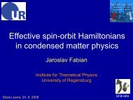
<strong>Fundamental</strong> <strong>concepts</strong> <strong>of</strong><br />
<strong>spintronics</strong><br />
Jaroslav Fabian<br />
Institute for Theoretical Physics<br />
University <strong>of</strong> Regensburg<br />
Stara Lesna, 24. 8. 2008 SFB 689
:outline:<br />
• what is <strong>spintronics</strong>?<br />
• spin injection<br />
• spin-orbit coupling in solids (next lecture)<br />
• spin devices<br />
• conclusions: challenges<br />
I. Zutic, J. Fabian, and S. Das Sarma,<br />
Spintronics: <strong>Fundamental</strong>s and applications, Rev. Mod. Phys. 76, 323 (2004)<br />
J. Fabian, A. Matos-Abiague, C. Ertler, P. Stano, and I. Zutic,<br />
Semiconductor <strong>spintronics</strong>, Acta Phys. Slov, 57, 566 (2007)
what is <strong>spintronics</strong>?<br />
narrow (device):<br />
electronics with spin<br />
broad:<br />
umbrella for electron spin<br />
phenomena in solids
<strong>spintronics</strong> drive<br />
technology<br />
fundamental<br />
discoveries
The Nobel Prize in Physics 2007<br />
The Royal Swedish Academy <strong>of</strong> Sciences has decided to award the<br />
Nobel Prize in Physics for 2007 jointly to<br />
Albert Fert<br />
Unité Mixte de Physique CNRS/THALES,<br />
Université Paris-Sud, Orsay, France<br />
Peter Grünberg<br />
Forschungszentrum Jülich, Germany,<br />
"for the discovery <strong>of</strong> Giant Magnetoresistance".
Giant MagnetoResistance<br />
P. Grunberg et al. (1988), A. Fert et al. (1988)<br />
small resistance<br />
large resistance<br />
multilayers 30 - 40% at RT
GMR hard disk read heads<br />
From: IBM web site
SPINTRONICS GOALS<br />
spin control <strong>of</strong> electrical properties<br />
(I-V characteristics)<br />
electrical control <strong>of</strong> spin<br />
(magnetization)
SPINTRONICS’ 3 REQUIREMENTS<br />
• EFFICIENT SPIN<br />
INJECTION<br />
F<br />
N<br />
• SLOW SPIN<br />
RELAXATION @<br />
SPIN CONTROL<br />
• RELIABLE SPIN<br />
DETECTION<br />
Silsbee-Johnson spin-charge coupling
:(electrical) spin injection:
Johnson-Silsbee spin injection experiment<br />
Silsbee: emf appears in the proximity <strong>of</strong> a ferromagnetic metal and spinpolarized<br />
nonmagnetic metal (inverse <strong>of</strong> spin injection)<br />
R. Silsbee, Bull. Mag. Reson. 2, 284 (1980)<br />
M. Johnson and R. H. Silsbee, Phys. Rev. Lett. 55, 1790 (1985).<br />
μ 0<br />
E E<br />
δM<br />
N (E) N (E) N (E) N (E)<br />
spin injection<br />
spin detection
visualizing spin injection<br />
S. A. Crooker et al., JAP, 101,081716 (2007)<br />
S. A. Crooker at al., Science 309, 2191 (2005)
spin injection into silicon<br />
I. Appelbaum et al, Nature 447, 295 (2007)<br />
I. Zutic and J. Fabian, Nature (NW) 447, 269 (2007)
spin injection into graphene<br />
single-layer on a SiO 2 substrate, room temperature<br />
N. Tombros, C. Jozsa, M. Popinciuc, H. T. Jonkman, and B. J. van Wees<br />
Electronic spin transport and spin precession in single graphene layers at room temperature,<br />
Nature 448, 571 (2007)<br />
N. Tombros, S. Tanabe, A. Veligura, C. Jozsa, M. Popinciuc, H. T. Jonkman, and B. J. van Wees<br />
Anisotropic spin relaxation in graphene, arXiv:0802.2892
Zincblende band structure (GaAs)<br />
optical orientation transitions<br />
(a)<br />
S 1/2<br />
E<br />
CB<br />
(b)<br />
P 3/2<br />
P 1/2<br />
Γ6<br />
Γ 8<br />
Γ 7<br />
E g<br />
Δ<br />
so<br />
HH<br />
LH<br />
SO<br />
0 k<br />
m j<br />
σ +<br />
−1/2 1/2<br />
3 1 1 3<br />
σ +<br />
CB<br />
σ− σ−<br />
−3/2 −1/2 1/2 3/2<br />
2 2<br />
−1/2 1/2<br />
SO<br />
HH,LH<br />
From: I. Zutic, J. Fabian, S. Das Sarma, Rev. Mod. Phys. 76, 323 (2004)
:spin relaxation:
:key <strong>concepts</strong>:<br />
spin relaxation and dephasing<br />
B<br />
Fe<br />
t=0, spin imbalance<br />
t=T 1 , spin balance<br />
impurity<br />
phonon<br />
spin-orbit<br />
coupling
:key <strong>concepts</strong>:<br />
spin relaxation and dephasing<br />
Bloch eqs
Time-resolved Faraday rotation<br />
Source: web site <strong>of</strong> Awschalom’s group<br />
ZnCdSe QW
mechanisms <strong>of</strong> spin relaxation<br />
Elliott-Yafet mechanism<br />
elemental metals and semiconductors<br />
Dyakonov-Perel mechanism<br />
Semiconductors without center <strong>of</strong> inversion<br />
symmetry<br />
Bir-Aronov-Pikus mechanism<br />
Heavily p-doped semiconductors<br />
Hyperfine interaction<br />
Electrons bound on impurity sites or confined<br />
In quantum dots<br />
J. Fabian, A. Matos-Abiague, C. Ertler, P. Stano, and I. Zutic,<br />
Semiconductor <strong>spintronics</strong>, Acta Physica Slovaca, 57, 565 (2007)
spin relaxation in bulk n-GaAs<br />
relaxation tim e(ns)<br />
τ<br />
τ<br />
τ<br />
τ<br />
τ<br />
τ<br />
R. I. Dzhioev et al., Phys. Rev. B 66, 245204 (2002)
spin relaxation in bulk n-Si<br />
100<br />
spin relaxation time T 1<br />
[ns]<br />
80<br />
60<br />
40<br />
20<br />
0<br />
7.4 10 14<br />
3.7 10 15<br />
4.5 10 15<br />
7.8 10 15<br />
2.7 10 16<br />
8.0 10 16<br />
0 50 100 150 200 250 300<br />
Temperature [K]<br />
D. Lepine, Phys. Rev. B 6, 436 (1972)<br />
J. Fabian, A. Matos-Abiague, C. Ertler, P. Stano, and I. Zutic, Acta Physica Slovaca, 57, 565 (2007)
:spin devices:<br />
(spin detection)
:semiconductor <strong>spintronics</strong> devices:<br />
• spin resonant diodes<br />
• spin field-effect transistors<br />
• magnetic semiconductor tunnel junction devices<br />
• magnetic bipolar junction diodes and transistors<br />
• spin optoelectronic devices<br />
• spin galvanics devices<br />
• spin Hall polarizeds<br />
• spin-polarized semiconductor lasers<br />
• spin pumping batteries<br />
• spin-torque devices<br />
• spin quantum computers<br />
• ...
J. Fabian, A. Matos-Abiague, C. Ertler, and P. Stano,<br />
Semiconductor <strong>spintronics</strong>, Acta Phys. Slov, 57, 566 (2007)
International Technology Roadmap<br />
2004<br />
for Semiconductors:<br />
Emerging Research Logic Devices<br />
RSFQ<br />
1-D<br />
structures<br />
resonant<br />
tunneling SET molecular QCA<br />
spin<br />
transistor<br />
risk<br />
2005, 2006
International Technology Roadmap<br />
2004<br />
for Semiconductors:<br />
Emerging Research Logic Devices<br />
RSFQ<br />
1-D<br />
structures<br />
resonant<br />
tunneling SET molecular QCA<br />
spin<br />
transistor<br />
risk<br />
2007
detour: material case study:<br />
GaMnAs<br />
• 5-15 % Mn<br />
• p-doped (Mn replaces Ga)<br />
• degenerate: p = 10 20 -10 21 /cm 3<br />
• Tc = 170 K<br />
• ferromagnetism and carrier density coupled<br />
• kλ about 3 (localization?)<br />
• impurity or valence band?<br />
• quantum coherence effects observed<br />
GaMnAs, from Jungwirth et al, Rev. Mod. Phys. 78, 809 (2006)
Where does GaMnAs fit?<br />
No good answer yet
magnetic Resonant Tunnel Diodes<br />
A. Slobodskyy et al, Phys. Rev. Lett. 90, 246601 (2003)<br />
C. Ertler and J. Fabian, Appl. Phys. Lett. 89, 193507 (2006)<br />
C. Ertler and J. Fabian, Phys. Rev. B 75 195323 (2007)<br />
ZnSe<br />
ZnSe<br />
BeZnSe<br />
BeZnSe<br />
ZnMnSe<br />
ZnMnSe<br />
b)<br />
ZnSe<br />
ZnSe<br />
Current (0-150 μA)<br />
8% Mn<br />
T=1.3K<br />
0T<br />
3T<br />
6T<br />
B<br />
1.3 K<br />
a)<br />
Voltage (0-0.2 V)<br />
• efficient spin filtering<br />
• spin detection<br />
• fast switching times<br />
• coherence issues<br />
• RT operation?<br />
Current Density (A/cm 2 )<br />
x 105 3<br />
Δ E = 0<br />
Δ E = 5 meV<br />
Δ E = 10 meV<br />
Δ E = 15 meV<br />
2.5<br />
T = 4.2 K<br />
Δ E = 20 meV<br />
Δ E = 25 meV<br />
Δ E = 40 meV<br />
2<br />
out<br />
ΔV 3<br />
1.5<br />
1<br />
100<br />
50<br />
0.5<br />
out<br />
ΔV 0<br />
2 0 10 20 30<br />
z (nm)<br />
0 out<br />
0 ΔV 0.05 0.1 0.15 0.2 1<br />
Voltage (V)<br />
0.25<br />
Energy (meV)
:selfsustained magneto-electric<br />
oscillations in MRTDs:<br />
C. Ertler and J. Fabian, Phys. Rev. Lett. 101, 077202 (2008)<br />
Intrinsic bistability leads to temporal oscillations in<br />
the current, magnetizaion, and particle density<br />
(a)<br />
x 10 15<br />
j max<br />
(b)<br />
20<br />
j (a.u.)<br />
(c)<br />
10<br />
5<br />
I<br />
j min<br />
0<br />
0 10 20 30<br />
Voltage (mV)<br />
x 10 15<br />
II<br />
j tot<br />
Δ (meV)<br />
(d)<br />
15<br />
10<br />
5<br />
I<br />
Δ max<br />
Δ min<br />
0<br />
0 10 20 30<br />
Voltage (mV)<br />
II<br />
n tot<br />
14 x 1011 Time (t*)<br />
j (a.u.)<br />
10<br />
5<br />
0<br />
j ↑<br />
j ↓<br />
50 100 150 200<br />
Time (t*)<br />
n (1/cm 2 )<br />
12<br />
10<br />
8<br />
6<br />
4<br />
2<br />
n ↑<br />
n ↓<br />
50 100 150 200
:nano<strong>spintronics</strong>:<br />
spin-based quantum information processing<br />
D. Loss and D. P. DiVincenzo, PRA 57, 120 (1998)<br />
• single and few spins manipulation and detection<br />
• spin relaxation and decoherence<br />
• entanglement control (EDAP: Fabian and Hohenester, PRB 72, 201304 (R) 2005)
closing: challenges in <strong>spintronics</strong><br />
• room-temperature ferromagnetic semiconductors, n and p type,<br />
identification <strong>of</strong> mechanisms for ferromagnetic long-range order<br />
• magnetic heterostructures: ferromagnetic quantum wells and quantum<br />
dots<br />
• spin-polarized transport through magnetic interfaces and inhomogeneities,<br />
accurate determination <strong>of</strong> spin polarization <strong>of</strong> ferromagnets<br />
• development <strong>of</strong> silicon (Si, Si:Ge) <strong>spintronics</strong>:<br />
spin injection, spin relaxation, magnetism (?), quantum dots<br />
• demonstration <strong>of</strong> semiconductor spin transistors--power gain and<br />
magnetologic:<br />
spin FETs, bipolar spin transistors<br />
• niche devices for GaMnAs or other dilute magnetic semiconductors,<br />
specific functionalities
closing: challenges in <strong>spintronics</strong><br />
• control <strong>of</strong> ferromagnetism by gating or current injection, spin-transfer<br />
torque<br />
• spin dynamics and spin pumping phenomena in spin transport<br />
• control <strong>of</strong> spin-orbit coupling by gate and doping, interface properties<br />
• single channel devices<br />
• Spin transport in carbon nanotubes, graphene<br />
• spin quantum information processing:<br />
single and few spin manipulation, relaxation and decoherence, spin<br />
entanglement control