book of abstracts - IM2NP
book of abstracts - IM2NP
book of abstracts - IM2NP

You also want an ePaper? Increase the reach of your titles
YUMPU automatically turns print PDFs into web optimized ePapers that Google loves.
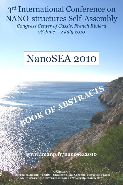
3 rd International Conference on<br />
NANO-structures Self-Assembly<br />
Congress Center <strong>of</strong> Cassis, French Riviera<br />
28 June – 2 July 2010<br />
NanoSEA 2010<br />
www.im2np.fr/nanosea2010<br />
Organisers :<br />
I. Berbezier, Im2np – CNRS – Université Paul Cézanne, Marseille, France<br />
M. De Crescenzi, Universita di Roma Tor Vergata, Roma, Italy
NANOSEA 2010<br />
International Conference
General Information ......................................................................................................................... 7<br />
Monday, June 28 .................................................................................................................................. 9<br />
Session 1 Room Calendal .................................................................................................................... 9<br />
Nanowires (Chairman: Lannoo).................................................................................................... 9<br />
Session 2 Room Calendal .................................................................................................................. 10<br />
Nanowires (Chairman: Vvedensky) ........................................................................................... 10<br />
Session 3 Room Port-Pin .................................................................................................................. 11<br />
Biomaterials (Chairman: Rowell) ................................................................................................. 11<br />
Tuesday, June 29 ................................................................................................................................. 29<br />
Session 4 Room Calendal ................................................................................................................. 29<br />
Near Field Microscopy (Chairman: Teichert) .......................................................................... 29<br />
Session 5 Room Calendal ................................................................................................................. 30<br />
Local Chemical and Structural Characterization (Chairman: Hillenbrand) .................. 30<br />
Session 6 Room Port-Pin ................................................................................................................. 31<br />
Si based Nanostructures (Chairman: Le Thanh) ..................................................................... 31<br />
Session 7 Room Port-Pin ................................................................................................................. 32<br />
Session Poster P1-P2 ........................................................................................................................ 33<br />
Wednesday, June 30 ......................................................................................................................... 58<br />
Session 8 Room Calendal ................................................................................................................. 58<br />
Organic Nanostructures (Chairman: De Crescenzi) ............................................................. 58<br />
Session 9 Room Calendal ................................................................................................................. 59<br />
Organic Nanostructures (Chairman: Porte) ............................................................................ 59<br />
Session 10 Room Port-Pin ............................................................................................................. 60<br />
Magnetic Nanostructuration (Chairman : )............................................................................. 60<br />
Session 11 Room Port-Pin ............................................................................................................. 61<br />
Zn-Based-Nanostructures (Chairman: Grosso) ........................................................................ 61<br />
3
Thursday, July 1 .................................................................................................................................... 79<br />
Session 12 Room Calendal ............................................................................................................. 79<br />
III-V Semiconductors (Chairman: Mesli) .................................................................................... 79<br />
Session 13 Room Calendal ............................................................................................................. 80<br />
Growth and Self Organisation (Chairman : Ters<strong>of</strong>f) .............................................................. 80<br />
Session 14 Room Calandar ............................................................................................................ 81<br />
Island (Chairman: Ronda) ............................................................................................................ 81<br />
Session 15 Room Port-Pin ............................................................................................................. 82<br />
Opto-Electronic Properties (Chairman: Del Sole)................................................................... 82<br />
Session 16 Room Port-Pin ............................................................................................................. 83<br />
Nanostructured Substrates (Chairman: Venables) ............................................................... 83<br />
Session 17 Room Port-Pin ............................................................................................................. 84<br />
Metallic Nanoparticles (Chairman: Fiorani) ............................................................................ 84<br />
Friday, July 2 ........................................................................................................................................ 116<br />
Session 18 Room Calendal ........................................................................................................... 116<br />
Mesoporous Systems (Chairman: )........................................................................................... 116<br />
Session 19 Room Calendal ........................................................................................................... 117<br />
Self Assembly (Chairman: Noguera) ....................................................................................... 117<br />
Session 20 Room Port-Pin ........................................................................................................... 118<br />
Carbon Nanotubes (Chairman: Berbezier) ........................................................................... 118<br />
Session 21 Room Port-Pin ........................................................................................................... 119<br />
Nanotubes and Coatings (Chairman: Goniakowski) ......................................................... 119<br />
4
NANOSEA 2010 International Conference<br />
NANOSEA 2010 International Conference is the third edition <strong>of</strong> NANOSEA, four years after the successful start<br />
in July 2006 in Aix-en-Provence , France (www.im2np.fr/nanosea2006/) and two years after NANOSEA 2008<br />
(www.nanosea2008.roma2.infn.it) held in the magnificent Villa Mondragone Conference Center , one <strong>of</strong> the most<br />
beautiful Tuscolum villas.<br />
NANOSEA 2010 will be held in the ancient fishing port <strong>of</strong> Cassis rebuilt in the 18th century situated at 20 km <strong>of</strong><br />
Marseilles . Cassis has become the most charming station along the coast surrounded by two exceptional domains :<br />
the Cap Canaille, highest european cliff (418m) and the Calanques, 23km <strong>of</strong> untouched rocky inlets until<br />
Marseille. The Congress Center <strong>of</strong> Cassis is located between the beach and the port and has an incredible view on<br />
the port with its boats and inviting terraces.<br />
General Information<br />
Research on nanostructures self-assembled encompasses fundamental issues in crystal growth and the scaling <strong>of</strong><br />
materials properties to molecular dimensions, and work on possible applications <strong>of</strong> nanoscale assemblies in<br />
advanced devices. The goal <strong>of</strong> this conference is to bring together the broad, multidisciplinary community <strong>of</strong><br />
researchers who are interested in the field <strong>of</strong> nanostructures and the opportunities for future high-impact science<br />
and technology related to such field.<br />
The Conference will provide a common forum for scientists operating in all the fields <strong>of</strong> nanostructures from their<br />
formation and modelling to their properties and applications. The conference will cover the physics <strong>of</strong><br />
nanostructures at the nanoscale, new fabrication procedures <strong>of</strong> nanostructures with well defined size, shape and<br />
composition, and also:<br />
- large-scale patterning obtained by spontaneous structuring as well as local probe nanopatterning for size and<br />
position control <strong>of</strong> nanostructures;<br />
- theoretical and experimental efforts dedicated to a better understanding <strong>of</strong> the formation, evolution and<br />
organisation <strong>of</strong> nanoscale systems;<br />
- fundamental and new issues in nucleation, crystal growth, surface and interface atomistic mechanisms and<br />
electronic structure;<br />
- optical, electrical, magnetic and mechanical properties representative <strong>of</strong> the self-assembled systems; Novel<br />
properties induced by low scale nanostructures.<br />
Finally, new insights on short-term and future/futuristic device applications will be <strong>of</strong> prime interest in the<br />
framework <strong>of</strong> this Conference.<br />
5
Scope<br />
NANOSEA 2010 will primarily focus on the following topics that are <strong>of</strong> strong current interest in fields <strong>of</strong><br />
nanostructures self-assembling and nanopatterned substrate:<br />
Nanostructured Materials :<br />
- Semiconductor - Metallic - Organic - Biological - New materials and structures<br />
Nanostructures classes :<br />
- Quantum dots, quantum wires and quantum wells - Nanotubes and nanorods - Nanoparticles and<br />
Nanoprecipitates - Nanoporous material - Very thin multilayers and superlattices<br />
Local structure <strong>of</strong> nanostructures :<br />
- Effects <strong>of</strong> local structure on properties in nanostructured materials - Quantitative characterization <strong>of</strong><br />
atomic arrangements - Characterization <strong>of</strong> nanoparticle surfaces - Characterization <strong>of</strong> internal interfaces<br />
Self-assembling techniques :<br />
- Nanopatterning by lithographic techniques - Ion-beam lithography and patterning - Nanopore<br />
fabrication and Pore filling - Substrate nanostructuring - Co-polymer template - Surface passivation -<br />
Functionalisation and catalysts – Nan<strong>of</strong>abrication<br />
Modelling :<br />
- Self-organisation and pattern formation - Thermodynamics and kinetics <strong>of</strong> nucleation and growth - Ab<br />
initio theory for spintronic materials and spin transport - Defects and impurities - Non-radiative and relaxation<br />
processes – Transport<br />
Properties :<br />
- Electronic and optical - Magnetic - Size dependent properties and transport - Mechanical - Structure,<br />
microstructure, and morphology<br />
Applications :<br />
- Novel microelectronic device - Nanoelectronic devices - Molecular devices - Nanodevice fabrication<br />
technology, characterization, properties and modelling - Photonic and photovoltaic devices - Chemical and<br />
biological sensors - Multifunctional spin devices - Magnetic random access memories (MRAM) - Other<br />
applications in medicine, biology, energy and environment …<br />
Web site : www.im2np.fr/nanosea2010<br />
6
Committees<br />
International Scientific Committee<br />
Aziz Univ. Harvard U.S.A. maziz@harvard.edu<br />
Bensahel STMicroelectronics France daniel.bensahel@st.com<br />
Del Sole Uni. Tor Vergata Italy Rodolfo.delsole@roma2.infn.it<br />
Kasper Erich Uni. Stuttgart Germany<br />
Kelires Univ. Crete Greece kelires@physics.uoc.gr<br />
Nogera INSP Insitut des Nanosciences de Paris France noguera@insp.jussieu.fr<br />
Nozaki Univ. Electro-Commun. Japan nozaki@ee.uec.ac.jp<br />
Nylandsted Larsen Univ. Aarhus Denmark anl@phys.au.dk<br />
Porte <strong>IM2NP</strong> France louis.porte@im2np.fr<br />
Ronda <strong>IM2NP</strong> France Antoine.ronda@im2np.fr<br />
Rowell NRC Canada nelson.rowell@nrc-cnrc.gc.ca<br />
Valbusa Univ. Genova Italy Valbusa@fisica.unige.it<br />
Valeri Univ. Modena Italy valeri@unimo.it<br />
Vveddensky Imperial College UK d.vvedensky@imperial.ac.uk<br />
Wiesendanger Univ. Hambourg Germany rwiesend@physnet.uni-hamburg.de<br />
Zanoni Uni. Roma La Sapienza Italy robertino.zanoni@uniroma1.it<br />
Organizing Committee<br />
Guillaume Amiard, Uni Paul Cézanne, CNRS, Marseilles France<br />
Mansour Aouassa, Uni Paul Cézanne, Marseilles France and Uni Monastir, Tunisia<br />
Franck Bassani , Uni Paul Cézanne, CNRS, Marseilles France<br />
Paola Castrucci, Uni Roma Tor Vergata, Italy<br />
Luc Favre , Uni Paul Cézanne, CNRS, Marseilles France<br />
Philippe Ferrandis , Uni Paul Cézanne, CNRS, Marseilles France<br />
Elise Gomes, Uni Paul Cézanne, CNRS, Marseilles France<br />
Adrien Gouyé, Uni Paul Cézanne, CNRS, Marseilles France<br />
Cathy Paitel, CNRS, Marseilles France<br />
Stéphane Riou, CNRS, Marseilles France<br />
Manuela Angela Scarselli, Uni Roma Tor Vergata, Italy<br />
Chairpersons<br />
Isabelle Berbezier<br />
Im2np - CNRS<br />
Marseilles, France<br />
Maurizio De Crescenzi<br />
Universita Di Roma<br />
Tor Vergata, Roma, Italy<br />
7
P R O G R A M MONDAY, JUNE 28 N A N O S E A 2 0 1 0<br />
Monday, June 28<br />
Session 1<br />
Room Calendal<br />
Nanowires (Chairman: Lannoo)<br />
10h00-10h30<br />
Introduction Speech<br />
Michel Lannoo<br />
10h30-11h10<br />
J. Ters<strong>of</strong>f (IBM Watson Research Center Yorktown Heights NY 10598 USA)<br />
Nanoscale phase transitions and nanowire growth<br />
11h10-11h30<br />
S. Tatarenko (Nanophysics and Semiconductors Group, INAC and Institut NEEL, CEA/CNRS/University<br />
Joseph Fourier, France)<br />
Microstructure and compositional study <strong>of</strong> MBE grown ZnSe NWs with CdSe<br />
inclusions<br />
11h30-11h50 Del Sole ((1) Laboratoire des Solides Irradies, Ecole Polytechnique - CNRS<br />
(2) Dip. di Fisica, CNISM, Universita‟ di Roma Tor Vergata, Roma, Italy<br />
(3) Dip. di Scienze e Metodi dell'Ingegneria, Università di Modena e Reggio Emilia, Italy<br />
(4) European Theoretical Spectroscopy Facility)<br />
Many body approach for the excitonic effects in 1D and 2D silicon doped<br />
nanostructures<br />
11h50-12h20<br />
Depadova (1CNR-ISM, via Fosso del Cavaliere, 00133 Roma, Italy; 2Instituto de Ciencia de Materiales de<br />
Madrid, CSIC, Cantoblanco 28049 Madrid, Spain; 3MAX-Lab, Lund University, Box 118 221 00 Lund, Sweden;<br />
4Consiglio Nazionale delle Ricerche-ISAC, via Fosso del Cavaliere, 00133 Roma, Italy; 5CINaM-CNRS, Campus<br />
de Luminy, Case 913, 13288 Marseille Cedex 9, France)<br />
One-dimensional Mn nano-wires on a ordered array <strong>of</strong> silicon nano-ribbons<br />
12h20-12h50<br />
Kawai (8-1,Mihogaoka, Ibaraki, Osaka, Japan)<br />
Self-assembled metal oxide Nanowires: Synthesis, Properties and Non-voltile<br />
Memory Applciations<br />
12h50-17h00<br />
Lunch and Break<br />
9
P R O G R A M MONDAY, JUNE 28 N A N O S E A 2 0 1 0<br />
Session 2<br />
Room Calendal<br />
Nanowires (Chairman: Vvedensky)<br />
17H00-17H30<br />
Calarco (1 Institute <strong>of</strong> Bio- and Nanosystems (IBN-1), Research Centre Jülich GmbH, 52425 Jülich, Germany,<br />
and JARA-FIT Fundamentals <strong>of</strong> Future Information Technology. 2 Center for Functional Nanomaterials,<br />
Brookhaven National Laboratory, Upton, New York 11973. 3 Phys. Department and CNISM, University <strong>of</strong> Bologna,<br />
Viale Berti Pichat 6/2, 40127 Bologna, Italy.)<br />
Nitride nanowires: from nucleation to optoelectrical measurements<br />
17H30-17H50<br />
Buick (1 Dipartimento di Fisica, CNISM, Universita‟ di Roma Tor Vergata, 00133 Roma, Italy. 2 IMM-CNR,<br />
Unità di Lecce, Via Arnesano, 73100 Lecce, Italy. 3 CNISM, and Dipartimento di Ingegneria dell‟Innovazione,<br />
Università del Salento, Via Arnesano, 73100 Lecce, Italy)<br />
Probing Single AlGaAs Core-Shell Nanowires by Raman Spectroscopy<br />
17H50-18H10 Carratero (1. Institut de Ciència de Materials de Barcelona-CSIC, Campus UAB, 08193 Bellaterra, Spain2. 2<br />
Université Catholique de Louvain, B-1340 Louvain la Neuve, Belgium)<br />
Synthesis and self-assembled <strong>of</strong> 1-D nanostructures based on La0.3Sr0.7MnO3 from<br />
template directed chemical solution deposition<br />
18H10-18H30<br />
Gibert (Institut de Ciència de Materials de Barcelona, ICMAB-CSIC, 08193 Bellaterra, Catalonia, Spain)<br />
Self-organized Ce1-xGdxO2-y Nanowire Networks with Ultrafast Coarsening<br />
resulting from Anisotropic Strain<br />
18H30-18H50<br />
Boarino (1 NanoFacility Piemonte, Electromagnetism Division, Istituto Nazionale di Ricerca Metrologica, Strada<br />
delle Cacce 91 - 10135 Turin, Italy2 Dept. <strong>of</strong> Structural and Geotechnical Eng., Politecnico di Torino, C.so Duca<br />
degli Abruzzi 24 - 10148Turin, Italy)<br />
Fabrication <strong>of</strong> Ordered Silicon Nanowires by Self-Assembling and Metal Assisted<br />
Etching<br />
18H50-19H10<br />
Tanemura (1. Guangzhou Institute <strong>of</strong> Energy Conversion, Chinese Academy <strong>of</strong> Sciences, No.2 Nengyuan Road,<br />
Wushan, Tianhe district, Guangzhou, 510640, P.R.China; 2. Japan Fine Ceramic Center, 2-4-1 Mutsuno, Atsuta-ku,<br />
Nagoya 456-8587, Japan; 3. Key Laboratory <strong>of</strong> Polarized Materials and Devices, Ministry <strong>of</strong> Education, East China<br />
Normal University, Shanghai 200062, China). miaolei@ms.giec.ac.cn, *tanemura-sakae@jfcc.or.jp,<br />
rhuang@ee.ecnu.edu.cn<br />
Synthesis <strong>of</strong> cation-intercalated titanate nanobelts.<br />
10
P R O G R A M MONDAY, JUNE 28 N A N O S E A 2 0 1 0<br />
Monday, June 28<br />
Session 3<br />
Room Port-Pin<br />
Biomaterials (Chairman: Rowell)<br />
17H00-17H30<br />
Iyer (Centre for Strategic Nano-fabrication, School <strong>of</strong> Biomedical, Biomolecular and Chemical Sciences, The<br />
University <strong>of</strong> Western Australia, 35 Stirling Highway, Crawley WA 6009, Australia; 2 Experimental and<br />
Regenerative Neurosciences, School <strong>of</strong> Animal Biology, The University <strong>of</strong> Western Australia, 35 Stirling Highway,<br />
Crawley WA 6009, Australia; 3 School <strong>of</strong> Anatomy and Human BiologyThe University <strong>of</strong> Western Australia, 35<br />
Stirling Highway, Crawley WA 6009, Australia)<br />
Applications <strong>of</strong> Nano-assembly in Neuroscience: From Multimodal Imaging to<br />
Regenerative Scaffolds<br />
17H30-17H50 Chang (Korea Institute <strong>of</strong> Ceramic Engineering and technology, 233-5 Gasan-dong, Guemcheon-gu, Seoul, 153-<br />
801, Korea)<br />
Functionalized Magnetic Nanomaterials for Clinical Bio-separation<br />
17H50-18H10<br />
HE (1 CNRS ; LAAS ; 7, avenue du Colonel Roche, F-31077 Toulouse, France2 Université de Toulouse ; UPS,<br />
INSA, INP, ISAE ; LAAS-CNRS : F-31077 Toulouse, France)<br />
Micropatterned poly-acrylamid gels for colloids self assembly and bio-assays.<br />
18H10-18H30<br />
Amdursky.(†Department <strong>of</strong> Molecular Microbiology and Biotechnology, George S. Wise Faculty <strong>of</strong> Life<br />
Sciences, Tel Aviv University, Tel Aviv, 69978, Israel‡Department <strong>of</strong> Electrical Engineering-Physical Electronics,<br />
School <strong>of</strong> Engineering, Tel Aviv University, Tel Aviv, 69978, Israel)<br />
Quantum Confinement approach for the self-assembly process <strong>of</strong> peptide and<br />
proteins structures<br />
18H30-18H50<br />
Roth (1HASYLAB-DESY, Notkestr. 85, D-22607 Hamburg, Germany; 2TU-Muenchen, Physik-Department<br />
Lehrstuhl E13, Garching, Germany; 3K.U. Leuven, Afdeling Kern- en Stralingsfysica, 3001 Heverlee, Belgium)<br />
Creating bi<strong>of</strong>ibre-noble metal nanocomposites - an in situ sputter deposition<br />
investigation<br />
18H50-19H10<br />
Severac (LAAS-CNRS - 7, avenue du Colonel Roche 31077 Toulouse Cedex 4 FRANCE.)<br />
Toward multifunctional energetic materials nanostructuration through DNA directed<br />
nanoparticles self assembly.<br />
11
A B S T R A C T S MONDAY, JUNE 28 N A N O S E A 2 0 1 0<br />
Room Calendal<br />
10h30-11h10<br />
Nanoscale phase transitions and nanowire growth.<br />
J. Ters<strong>of</strong>f (IBM Watson Research Center Yorktown Heights NY 10598 USA)<br />
Semiconductor nanowires can be readily grown from tiny catalyst particles. These wires, with diameters as<br />
small as a few nanometers, have attracted intense interest due to their potential applications in nanoscale<br />
technologies. At the same time, they <strong>of</strong>fer a unique opportunity to deepen our understanding <strong>of</strong> crystal<br />
growth. It has long been realized that novel effects are expected for growth at the nanoscale. But only<br />
recently has it become possible to measure these effects directly, using in-situ microscopy.<br />
This talk will describe some recent progress in understanding growth at the nanoscale, by combining<br />
experimental observations, theoretical modeling, and direct computer simulation <strong>of</strong> nanowire growth [1-3].<br />
We studied the sequence <strong>of</strong> phase transformations as a Au seed particle is exposed to disilane to initiate<br />
nanowire growth. On an inert substrate and above the eutectic temperature, the system progresses from Au<br />
to a two-phase Au+AuSi eutectic system, to liquid AuSi, and finally to AuSi+Si, initiating nanowire growth<br />
[2,3]. By comparing the experimental measurements with a simple theoretical model, we determine the<br />
changes in the equilibrium phase diagram for nanoscale systems, and the effect <strong>of</strong> system size on the<br />
nucleation process. We also find dramatic deviations from equilibrium due to kinetic effects in nanowire<br />
growth. We have developed a theoretical model for the eutectic system evolution, allowing direct computer<br />
simulation <strong>of</strong> nanowire growth [3]. These simulations shed light on how material properties and growth<br />
conditions control the wire morphology and growth stability [3].<br />
* Work done in collaboration with K.W. Schwarz, B.J. Kim, S. Kodambaka, E.A. Stach, and F.M. Ross.<br />
[1] B. J. Kim, J. Ters<strong>of</strong>f, S. Kodambaka, M. C. Reuter, E. A. Stach, and F. M. Ross, Science 322, 1070 (2008).<br />
[2] K. W. Schwarz and J. Ters<strong>of</strong>f, Phys. Rev. Lett. 102, 206101 (2009).<br />
[3] B. J. Kim, J. Ters<strong>of</strong>f, C.-Y. Wen, M. C. Reuter, E. A. Stach, and F. M. Ross, Phys. Rev. Lett. 103, 155701 (2009)<br />
11h10-11h30<br />
Microstructure and compositional study <strong>of</strong> MBE grown ZnSe NWs with<br />
CdSe inclusions.<br />
S. Tatarenko (Nanophysics and Semiconductors Group, INAC and Institut NEEL, CEA/CNRS/University<br />
Joseph Fourier, France) serge.tatarenko@grenoble.cnrs.fr<br />
We have recently shown that a single CdSe quantum dot embedded in a ZnSe nanowire (NW) is an efficient<br />
single photon source operating at a temperature as high as 220K [1]. However, when grown on an oxidized<br />
Si (001) substrate in the VLS growth mode catalyzed by gold particles, the NWs present a random<br />
distribution <strong>of</strong> orientations and densities.<br />
In this contribution we report on the epitaxial growth <strong>of</strong> ZnSe/CdSe NWs on 2D epitaxial ZnSe (100) on<br />
GaAs (100) substrate. Scanning electron microscopy (SEM) and High Resolution Transmission Electron<br />
Microscopy (HRTEM) images (Fig 1) show ZnSe NWs with hexagonal wurtzite structure along the [0001]<br />
axis and also NWs with cubic zinc-blende structure along the [100] axis. The presence <strong>of</strong> different NW<br />
orientations is attributed in part to the formation <strong>of</strong> [110] oriented nanotrenches generated by Au dewetting<br />
at 530°C [2, 3]. The first steps <strong>of</strong> the growth for both growth directions will be presented in details as well<br />
as the influence <strong>of</strong> the growth parameters.<br />
12
A B S T R A C T S MONDAY, JUNE 28 N A N O S E A 2 0 1 0<br />
The microstructure <strong>of</strong> NWs including a CdSe quantum dot has been studied in detail by HRTEM. In Fig. 2<br />
the ZnSe NW adopts the hexagonal wurtzite-type structure with growth along the [0001] axis. The CdSe<br />
inclusions were identified by Energy Dispersive X-ray spectroscopy as well as by interplanar spacing<br />
variations along the wire axis obtained by the Geometrical Phase Analysis <strong>of</strong> an HRTEM micrograph.<br />
Energy Filtered TEM image demonstrate the absence <strong>of</strong> Zn in the CdSe region indicating limited<br />
interdiffusion (Zn map in Fig. 3a). It is worth noting that in this NW, the crystalline structures <strong>of</strong> the ZnSe<br />
part and inclusion part are opposite to their bulk-form case, know to be cubic and hexagonal for ZnSe and<br />
CdSe respectively.<br />
For the same deposition time, the CdSe inclusions are as small as 1.5nm long when growth occurs at 450°C<br />
(Fig. 2b), while the inclusion length can reach 20nm for growth at 400°C (Fig. 3). This result opens the way<br />
to a control over the shape (disk or cylinder) <strong>of</strong> the inclusion, and consequently on the tuning <strong>of</strong> its optical<br />
properties (wavelength, polarisation, efficiency…). Finally we will present the PL results obtained on single<br />
NWs with CdSe insertion <strong>of</strong> different lengths.<br />
[1] A. Tribu et al. Nano Lett. 8, 4326 (2008)<br />
[2] S.K. Chan et al, Appl. Phys. Lett. 92, 183102 (2008)<br />
[3] E. Bellet-Amalric et al in press<br />
b<br />
Hexagonal<br />
c<br />
Cubic<br />
8 nm<br />
10 nm<br />
Figure 1 - SEM image (a) and TEM images <strong>of</strong> a hexagonal (b) and a cubic (c) ZnSe nanowires grown on a ZnSe (001) buffer layer<br />
b<br />
a<br />
c<br />
Figure 2<br />
(a) HRTEM image <strong>of</strong> a ZnSe nanowire<br />
with a CdSe insertion grown at 450°C.<br />
(b) Zoom <strong>of</strong> the inset showing the<br />
wurzite / zinc blende transition<br />
(c) Map <strong>of</strong> the d-spacing along the<br />
growth axis obtained for the same wire<br />
Figure 3 - TEM (A, B) and EFTEM (C) <strong>of</strong> a ZnSe NW with a CdSe insertion<br />
grown at 400°C.<br />
13
A B S T R A C T S MONDAY, JUNE 28 N A N O S E A 2 0 1 0<br />
11h30-11h50<br />
Many body approach for the excitonic effects in 1D and 2D silicon doped<br />
nanostructures.<br />
Del Sole ((1) Laboratoire des Solides Irradies, Ecole Polytechnique - CNRS<br />
(2) Dip. di Fisica, CNISM, Universita‟ di Roma Tor Vergata, Roma, Italy<br />
(3) Dip. di Scienze e Metodi dell'Ingegneria, Università di Modena e Reggio Emilia, Italy<br />
(4) European Theoretical Spectroscopy Facility)<br />
Silicon Nanowires (Sinw) and Silicon Nanoribbons (Sinr) are one- (1D) and two- (2D) dimensional<br />
nanostructures which are attracting in the last years increasing interest for potential nanoelectronic and<br />
nanophotonic applications. Sinw have made an impact in applications in fields as diverse as electronics,<br />
photonic, sensing, biology and photovoltaics , while Sinr, recently realized, seems to be promising as well,<br />
maybe even more than the 1D systems for silicon basednanotechnology application.<br />
In this theoretical work we investigate mainly the electronic and the optical properties <strong>of</strong> 1D and 2D system<br />
with and without the presence <strong>of</strong> impurities. The size and doping dependence <strong>of</strong> the electron-hole exchange<br />
interaction in Si nanowires is investigated from first-principles. In pure Si nanowires we found excitonic<br />
exchange splittings in very good agreement with the experimental results for porous silicon. For n-doped Si<br />
nanowires a giant singlet-triplet splitting, three order <strong>of</strong> magnitude bigger than in bulk silicon, is predicted as<br />
due to the dramatic enhancement <strong>of</strong> the electron and the hole probability <strong>of</strong> being in the same place at the<br />
same time. For the Sinr we have calculated the dielectric function for different light polarization in and<br />
outside the plane by taking into account many body effect.<br />
11h50-12h20<br />
One-dimensional Mn nano-wires on a ordered array <strong>of</strong> silicon nanoribbons.<br />
P. De Padova1, M. E. Dávila2, F. Hennies3, A. Pietzsch3, N. Shariati3, C.<br />
Ottaviani1, C. Quaresima1, B. Olivieri4, F. Ronci1, S. Colonna1, A. Cricenti1, B.<br />
Aufray5, G. Le Lay5 (1CNR-ISM, via Fosso del Cavaliere, 00133 Roma, Italy. 2Instituto de Ciencia de<br />
Materiales de Madrid, CSIC, Cantoblanco 28049 Madrid, Spain. 3MAX-Lab, Lund University, Box 118 221 00<br />
Lund, Sweden. 4Consiglio Nazionale delle Ricerche-ISAC, via Fosso del Cavaliere, 00133 Roma, Italy. 5CINaM-<br />
CNRS, Campus de Luminy, Case 913, 13288 Marseille Cedex 9, France)<br />
Silicon nano-ribbons (SiNRs) are one <strong>of</strong> the more promising systems for studying the role <strong>of</strong> dimensionality<br />
on physical properties for potential applications in nanoscale electronics or spintronics. Room temperature<br />
(RT) deposition <strong>of</strong> low coverages <strong>of</strong> Si on the Ag(110) surface produces massively parallel Si nano-ribbons<br />
(SiNRs) along the [–110] direction. They have a magic width <strong>of</strong> 16 Å, unprecedented spectral signatures in<br />
valence band and core-level spectroscopy and unique burning match-like oxidation behavior. Upon<br />
annealing, a very well ordered array <strong>of</strong> SiNRs, in a 5x2/5x4 arrangement, is obtained on the Ag(110)<br />
substrate.<br />
Si was evaporated on Ag(110) substrate at a rate <strong>of</strong> ~ 0.03 ML/min from a Si source, while the sample was<br />
heated at 440 K to obtain a dense array SiNRs (5x2/5x4 reconstruction). LEED observations were used to<br />
monitor the x2 and 5x2/5x4 superstructures.<br />
Core level spectroscopy data have been taken at the VUV beamline <strong>of</strong> ELETTRA (Trieste). The photon<br />
energies used for Si 2p core level was 135.8 eV.<br />
Here we report the electronic and structural properties <strong>of</strong> Mn grown on a dense array <strong>of</strong> well-ordered SiNRs<br />
on Ag(110). High-resolution Si 2p core levels show an interesting selective adsorption <strong>of</strong> Mn atoms on the<br />
SiNRs as clearly evidenced by the collection <strong>of</strong> high-resolution scanning tunneling microscopy images. We<br />
14
A B S T R A C T S MONDAY, JUNE 28 N A N O S E A 2 0 1 0<br />
found an unusual one-dimensional growth <strong>of</strong> Mn on top <strong>of</strong> the dense array <strong>of</strong> SiNRs, which act s as a<br />
template at atomic scale.<br />
The Si 2p spectrum <strong>of</strong> the Si/Ag(110)5 2/5x4 reconstruction shows two main components, S1 and S2 as<br />
those reported [1,2] for the Si/Ag(110) 2 one. After the adsorption <strong>of</strong> Mn a new reacted component, RMn-<br />
Si, chemically shifted by 0.45 eV towards higher kinetic energy (32.5 eV), is clearly evident. Interestingly,<br />
one notices that the Mn atoms affect only the S2 component; in fact, the S1 is absolutely unaltered. This<br />
shows that the Mn atoms are adsorbed preferentially on just one Si site and, consequently, that they form<br />
straight Mn-Si nanostripes along the [-110] direction on the Si/Ag(110)5 2/5x4 substrate.<br />
We studied the Mn adsorption on dense array <strong>of</strong> Si NRs grown on Ag(110) by STM and Si 2p core level<br />
spectroscopy. Very interesting one-dimensional Mn nano-wires were realized.<br />
12h20-12h50<br />
Self-assembled metal oxide Nanowires: Synthesis, Properties and Nonvoltile<br />
Memory Applciations.<br />
T. Kawai (8-1,Mihogaoka, Ibaraki, Osaka, Japan)<br />
Self-assembled Metal oxides nanowires are potential candidates towards functional nanowire-based devices<br />
due to their fascinating physical properties, including resistive switching memory effect. Within the<br />
framework <strong>of</strong> conventional vapor-liquid-solid self-assembly mechanism to form the nanowires, there is a<br />
fundamental limitation to create diverse metal oxide nanowires. Heterostructured nanowires are most<br />
promising ways to overcome such difficulties. Our recent progress will be reported on the synthesis <strong>of</strong> selfassembled<br />
heterostructured nanowires using metal oxides, the transport properties, and the non-volatile<br />
memory applications. The oxide heterostructured nanowires were fabricated by in-situ laser MBE technique<br />
taking advantage <strong>of</strong> seeds based self-assembly process that has been newly developed. Various kinds <strong>of</strong><br />
oxide heterostructured nanowires can be fabricated using the in-situ technique, TiO2/MgO, Fe3O4/MgO,<br />
NiO/MgO , MgO/Fe3O4/NiO. When forming the oxide heterostructured nanowires, the lattice matching in<br />
3D was found to be a crucial factor to fabricate the well-defined epitaxial heterointerface. The atomic intermixing<br />
at the heterointerface and the surface oxidization were found to play a crucial role on the transport<br />
properties <strong>of</strong> metal oxide nanowires. Furthermore, we found the resistive switching memory effect within the<br />
single metal oxide nanowire by utilizing nano-gap electrodes and C-AFM method. Thus the metal oxide<br />
nanowires are expected to open up opportunities to explore not only the detailed nanoscale properties <strong>of</strong><br />
metal oxides but also next-generation nanoscale oxide devices with the potential <strong>of</strong> high-density device<br />
integration and the improved device characteristics.<br />
[1] Appl. Phys. Lett., 90, 233103 (2007),<br />
[2] Appl. Phys. Lett., 91, 061502 (2007),<br />
[3] J. Appl. Phys., 101, 124304 (2007),<br />
[4] J. Appl. Phys., 102, 016102 (2007),<br />
[5] J. Am. Chem. Soc., 130, 5378 (2008),<br />
[6] Appl. Phys. Lett., 92, 173119 (2008),<br />
[7] J. Appl. Phys., 104, 016101 (2008),<br />
[8] J. Appl. Phys., 104, 013711 (2008),<br />
[9] Appl. Phys. Lett., 93, 153103 (2008),<br />
[10] J. Phys. Chem. C, 112, 18923 (2008),<br />
[11] J. Am. Chem. Soc., 131, 3434 (2009)<br />
15
A B S T R A C T S MONDAY, JUNE 28 N A N O S E A 2 0 1 0<br />
Room Calendal<br />
17H00-17H30<br />
Nitride nanowires: from nucleation to optoelectrical measurements<br />
R. Calarco, Toma Stoica1, Eli Sutter2, Ralph Meijers1, Thomas Schäpers1, Thomas<br />
Richter1, Ratan K. Debnath1, Michel Marso1, Hans Lüth1, A. Cavallini3, L.<br />
Polenta3, M. Rossi3. (1 Institute <strong>of</strong> Bio- and Nanosystems (IBN-1), Research Centre Jülich GmbH, 52425<br />
Jülich, Germany, and JARA-FIT Fundamentals <strong>of</strong> Future Information Technology. 2 Center for Functional<br />
Nanomaterials, Brookhaven National Laboratory, Upton, New York 11973. 3 Phys. Department and CNISM,<br />
University <strong>of</strong> Bologna, Viale Berti Pichat 6/2, 40127 Bologna, Italy.)<br />
1 – Introduction<br />
In recent years III-nitride based nanowires have attracted a lot <strong>of</strong> interest because <strong>of</strong> their potential<br />
applications for nanoelectronic devices [1-5]. III-nitride NWs are indeed extremely interesting due to the fact<br />
that on the one hand they possess impressive material properties and on the other hand they constitute a 1D<br />
structure. The combination <strong>of</strong> both aspects <strong>of</strong>fers the possibility <strong>of</strong> studying fundamental issues <strong>of</strong> transport<br />
properties, <strong>of</strong>ten with tight feed back to the optimization <strong>of</strong> growth.<br />
2 – Abstract<br />
We showed that the growth <strong>of</strong> Nitride nanowires by MBE occurs on various substrates under appropriate<br />
growth conditions without using a liquid-phase catalyst, i.e. a droplet, at the top <strong>of</strong> the growing nanowire.<br />
We addressed the optimization [6, 7] <strong>of</strong> the crystalline and optical quality <strong>of</strong> nitride nanowires as well as the<br />
nucleation, kinetics and growth mechanisms [8, 9]. We observed that the growth is characterized by a long<br />
nucleation period [8], which results in a broad distribution <strong>of</strong> the nanowire sizes. A diffusion mechanism was<br />
found to dominate the NW growth after the nucleation period and can explain the diameter dependence <strong>of</strong><br />
the NW length [9]. In addition, it was demonstrated that nanowire growth occurs perpendicular to the<br />
substrate surface and along the crystallographic c-axis even on non-crystalline amourphous SiO2 substrates<br />
[10]. This last statement has a tremendous importance and opens new possibilities for NW growth on a<br />
variety <strong>of</strong> nonconventional substrates <strong>of</strong> interest for applications relying on low-cost substrates. Numerous<br />
structures, including GaN and InN nanowires, GaN/AlGaN hetero- and quantum structures as well as<br />
InN/GaN core-shell structures were realized over the past years.<br />
The high quality <strong>of</strong> the material allowed for studying fundamental transport properties. In our work<br />
particular emphasis was given to the investigation <strong>of</strong> effects due to surface space charge layers. Therefore,<br />
we especially focused on both narrow gap (InN) and wide band gap (GaN) materials in which accumulation<br />
and depletion space charge layers are present at the surface, respectively.<br />
The investigation <strong>of</strong> the electrical properties <strong>of</strong> GaN nanowires showed that the band-to-band photoelectric<br />
effect varies by orders <strong>of</strong> magnitude as a function <strong>of</strong> the nanowire diameter [4]. For these studies, single<br />
nanowire devices were fabricated using e-beam lithography for the preparation <strong>of</strong> metallic contacts. The<br />
unusual effect which we found was explained by modeling <strong>of</strong> the effect <strong>of</strong> the electron depletion region at<br />
the nanowire surface. Photovoltage Spectroscopy and Spectral Photoconductivity (SPC) measurements have<br />
been carried out to analyze the near band-edge absorption in GaN nanowires [11]. A strong diameter<br />
dependence <strong>of</strong> the band absorption tail was found by SPC measurements. The band-edge tailoring and its<br />
wire-diameter dependence can be explained by the Franz-Keldysh effect induced by the electric field at the<br />
wire surface.<br />
16
A B S T R A C T S MONDAY, JUNE 28 N A N O S E A 2 0 1 0<br />
In InN nanowires in contrast to GaN the Fermi-level pinning in the conduction band induces a highly<br />
conductive surface accumulation layer and as a result the nanowires display very high currents several orders<br />
<strong>of</strong> magnitude higher than in the GaN nanowires. In addition, the movement <strong>of</strong> the Fermi level within the<br />
conduction band results in changes <strong>of</strong> the photoluminescence (PL) peak position. Therefore, a detailed<br />
analysis <strong>of</strong> the PL spectra has been used to determine intrinsic properties <strong>of</strong> InN nanowires such as band gap<br />
and electron concentration and to pro<strong>of</strong> the existence <strong>of</strong> a surface accumulation layer [12]. InN nanowires<br />
additionally represent ideal systems for the observation <strong>of</strong> ballistic transport and quantum effects ona<br />
nanometer scale [13].<br />
3 – Conclusion<br />
The effect <strong>of</strong> surface Fermi-level pinning and its interplay with the nanowire dimensions on the<br />
recombination behavior <strong>of</strong> electron hole pairs in photoconductivity were investigated. The distinct transport<br />
properties <strong>of</strong> GaN and InN are explained by the different surface Fermi level pinning leading to surface<br />
depletion and accumulation for GaN and InN, respectively. Particular emphasis has been given to the<br />
investigation <strong>of</strong> effects due to space charge layers.The space charge could be used as a design parameter for<br />
novel devices concept.<br />
[1] A. Greytak, L. Lauhon, M. Gudiksen, and C. M. Lieber, Appl. Phys. Lett. 84, 4176 (2004).<br />
[2] S. Gradečak, F. Qian, Y. Li, H.-G. Park, and C. M. Lieber, Appl. Phys. Lett. 87, 173111 (2005).<br />
[3] Y. Huang, X. Duan, Y. Cui, L. J. Lauhon, K.-H. Kim, and C. M. Lieber, Science 294, 9, 1313 (2001).<br />
[4] R. Calarco, M., Marso, T. Richter, A. I. Aykanat, R. Meijers, A. v.d. Hart, T. Stoica, and H. Lüth, Nano Letters 5, 981 (2005).<br />
[5] A. Cavallini, L. Polenta, M. Rossi, T. Richter, M. Marso, R. Meijers, R. Calarco, and H. Lüth, Nano Letters, 6(7), 1548-1551 (2006).<br />
[6] R. Meijers, T. Richter, R. Calarco, T. Stoica, H.-P. Bochem, M. Marso, and H. Lüth, J. Cryst. Growth 289, 381 (2006).<br />
[7] T. Stoica, R. Meijers, R. Calarco, T. Richter, and H. Lüth, J. Cryst. Growth 290, 241 (2006).<br />
[8] R. Calarco, R. J. Meijers, R. K. Debnath, T. Stoica, E. Sutter and H. Lüth Nano Letters, 7 (8), 2248 -2251, (2007).<br />
[9] R. K. Debnath, R. Meijers, T. Richter, T. Stoica, R. Calarco and H. Lüth, Appl. Phys. Lett., 90, 123117 (2007).<br />
[10] T. Stoica, E. Sutter, R. Meijers, R. K. Debnath, R. Calarco, and H. Lüth Small 4, 751 (2008).<br />
[11] A. Cavallini, L. Polenta, M. Rossi, T. Stoica, R. Calarco, R. J. Meijers, T. Richter and H. Lüth Nano Letters, 7, 2166 (2007).<br />
[12] T. Stoica, R. Meijers, R. Calarco, T. Richter, E. Sutter, and H. Lüth,, Nano Letters, 6(7), 1541-1547 (2006).<br />
[13] T. Richter, C. Blömers, H. Lüth, R. Calarco, M. Indlek<strong>of</strong>er, M. Marso, and T. Schäpers, Nano Lett. 8, 2834 (2008).<br />
17H30-17H50<br />
Probing Single AlGaAs Core-Shell Nanowires by Raman Spectroscopy.<br />
B. Buick*1, E. Speiser1, P. Prete2, P. Paiano3, N. Lovergine3, and W. Richter1 (1<br />
Dipartimento di Fisica, CNISM, Universita‟ di Roma Tor Vergata, 00133 Roma, Italy. 2 IMM-CNR, Unità di Lecce,<br />
Via Arnesano, 73100 Lecce, Italy. 3 CNISM, and Dipartimento di Ingegneria dell‟Innovazione, Università del<br />
Salento, Via Arnesano, 73100 Lecce, Italy)* Corresponding author e-mail: benjamin.buick@roma2.infn.it<br />
1 – Introduction<br />
Semiconductor nanowires (NWs) <strong>of</strong> III-V compounds are <strong>of</strong> central interest due to their innovative physical<br />
properties and due to potential applications in electronic and photo-electronic devices. Ternary nanowires are<br />
promising because their properties can be tailored by the stoichiometry. Furthermore, nanowires containing<br />
axial/ radial homo- or heterojunction are especially interesting.<br />
2 – Abstract<br />
Freestanding AlGaAs NWs were grown by MOVPE by the Vapor Liquid Solid (VLS) method along the<br />
(111) direction on GaAs(111) substrates. Depending on the growth conditions, the nanowires show diameters<br />
< 100 nm or an unintetional/ intentional core-shell structure. Raman spectroscopy provides access to the<br />
vibrational/structural properties, carrier concentration (doping) and the material stoichiometry.<br />
17
A B S T R A C T S MONDAY, JUNE 28 N A N O S E A 2 0 1 0<br />
Raman measurements were done with a scanning confocal micro-Raman spectrometer providing both lateral<br />
(
A B S T R A C T S MONDAY, JUNE 28 N A N O S E A 2 0 1 0<br />
Fig. 1: Typical field emission SEM images <strong>of</strong> LSMO nanowires<br />
prepared using polyimide membranes with 100 nm pore size.<br />
The inset shows a magnified image.<br />
Fig. 2: SEMFE image <strong>of</strong> self-assembled.<br />
epitaxial LSMO monoclinic nanowires<br />
As a model system, La0.7Sr0.3MnO3 polycrystalline vertical nanorods in the range <strong>of</strong> 100 to 300 nm in<br />
lateral sizes and up to 1 µm in height have been also grown on STO and LAO single crystal substrates at<br />
mild temperatures (800 ºC), using a polycarbonate nanotemplate buffer layer. The nanorods suffer a<br />
pr<strong>of</strong>ound transfo rmation into vertical single crystalline (La,Sr)xOy nanopyramids sitting onto a LSMO<br />
epitaxial wetting layer, upon strong thermal activation (1000ºC). The driving force for this outstanding<br />
nanostructural evolution is the minimization <strong>of</strong> the total energy <strong>of</strong> the system that is reached by reducing the<br />
grain boundary energy and total surface and strain relaxation energies. Finally, advanced electron<br />
microscopy techniques were used to highlight the complex phase separation and structural transformation<br />
occurring when the metastable state is overcome [2].<br />
Fig. 3: SEM images <strong>of</strong> LSMO polycrystalline nanorods vertically grown on LAO substrate,<br />
In summary, this work establishes a method <strong>of</strong> preparing complex oxides nanostructures by sol-gel based<br />
polymeric precursor solution, using a totally novel version <strong>of</strong> track etched polymer directly buffering<br />
substrates, which is <strong>of</strong> the utmost importance and could be applied to any number <strong>of</strong> substrate thin film<br />
combinations. It allows nanostructuration <strong>of</strong> other functional complex oxide nanostructures; an issue that is<br />
widely pursed by the scientific community, to go beyond the complex and expensive top-down<br />
nanolithography methodologies required nowadays.<br />
We acknowledge the financial support from MICINN (MAT2008-01022, MAT2005-02047, MAT2006-<br />
26543-E, NAN2004-09133-CO3-01, Consolider NANOSELECT and FPI), Generalitat de Catalunya<br />
(Catalan Pla de Recerca SGR-0029 and XaRMAE), CSIC (PIF-CANNAMUS) and EU (HIPERCHEM,<br />
NMP4-CT2005-516858 and NESPA) for TEM facilities.<br />
[1] A. Carretero-Genevrier, N. Mestres, T. Puig, A. Hassini, J. Oro, A. Pomar, F. Sandiumenge, X. Obradors, E. Ferain, Adv Mater. 20,<br />
3672(2008).<br />
[2] A. Carretero-Genevrier, J. Gázquez, T. Puig, N. Mestres, F. Sandiumenge, X. Obradors, and E. Ferain , Adv. Funct. Mater.,<br />
10.1002/adfm.200901971(2009).<br />
19
A B S T R A C T S MONDAY, JUNE 28 N A N O S E A 2 0 1 0<br />
18H10-18H30<br />
Self-organized Ce1-xGdxO2-y Nanowire Networks with Ultrafast<br />
Coarsening resulting from Anisotropic Strain.<br />
M. Gibert, P. Abellán, F. Sandiumenge, T. Puig, X. Obradors (Institut de Ciència de<br />
Materials de Barcelona, ICMAB-CSIC, 08193 Bellaterra, Catalonia, Spain) mgibert@icmab.es<br />
1 – Introduction<br />
Assembling arrays <strong>of</strong> ordered nanowires is a key objective for many <strong>of</strong> their potential applications. However,<br />
a lack <strong>of</strong> understanding and control <strong>of</strong> the nanowires‟ growth mechanisms limits their thorough development.<br />
In this work, we report a new path towards self-organized epitaxial nanowires networks produced by high<br />
throughput solution methods.<br />
2 – Abstract<br />
Fine control <strong>of</strong> interfacial energy through growth conditions enables us to select the crystallographic<br />
orientation <strong>of</strong> Ce1-xGdxO2-y (CGO) nanostructures on perovskite substrates (i.e., LaAlO3 (LAO)),<br />
providing us with a powerful tool to study the formation <strong>of</strong> islands with different degree <strong>of</strong> lateral aspect<br />
ratio c. Self-organized and stable uniform square-based nanopyramids form when the crystallographic<br />
orientation (001)CGO[110]||(001)LAO[100] is promoted [1]. In contrast, anisotropically strained CGO<br />
nanowires are generated when the (011) orientation is grown on the (001) surface <strong>of</strong> the LAO single-crystals.<br />
As a result, self-organized anisotropic nanostructures with aspect ratios above ~100 oriented along two<br />
mutually orthogonal axes are obtained leading to labyrinthine networks. Detailed experimental analyses and<br />
thermodynamic modeling has enabled us to identify two requisites to generate such epitaxial nanowires; a<br />
thermodynamic driving force for an unrestricted elongated equilibrium island shape, and an ultrafast<br />
effective growth rate. Ultrafast coarsening (~60 nm min-1) derives from Ostwald ripening and anisotropic<br />
dynamic coalescence, both promoted by strain-driven attractive nanowire interaction, and from fast<br />
recrystallization enabled by rapid atomic diffusion associated to a high concentration <strong>of</strong> oxygen vacancies.<br />
3 – Conclusion<br />
Hence, we propose a new and high throughput approach to generate self-organized nanowire templates,<br />
which has a wide potential for many materials and functionalities. The thermodynamic origin and the kinetic<br />
mechanisms enabling their formation are fully scrutinized.<br />
[1] Gibert, M. et al., Adv.Materials 19, 3937 (2007).<br />
20
A B S T R A C T S MONDAY, JUNE 28 N A N O S E A 2 0 1 0<br />
18H30-18H50<br />
Fabrication <strong>of</strong> Ordered Silicon Nanowires by Self-Assembling and Metal<br />
Assisted Etching.<br />
L. Boarino1, E. Enrico1, N. De Leo1, F. Celegato1, P. Tiberto1, E. Lepore2 and N.<br />
Pugno2 (1 NanoFacility Piemonte, Electromagnetism Division, Istituto Nazionale di Ricerca Metrologica,<br />
Stradadelle Cacce 91 - 10135 Turin, Italy; E-mail: l.boarino@inrim.it; Tel: +39 (11) 39196402 Dept. <strong>of</strong> Structural<br />
and Geotechnical Eng., Politecnico di Torino, C.so Duca degli Abruzzi 24 - 10148Turin, Italy)<br />
1 – Introduction<br />
The field <strong>of</strong> silicon nanowires (SiNWs) saw, in the last years, a real boom in the number and quality <strong>of</strong><br />
publications. A part the basic research, investigating the most fundamental properties like electron transport1<br />
and mechanics2, several fields <strong>of</strong> application can take advantage from silicon nanowires, like energy, with<br />
photovoltaic devices <strong>of</strong> new generation3, energy harvesting by vibrations4 and new adhesives5. The recent<br />
development <strong>of</strong> the self-catalytic electroless etching in presence <strong>of</strong> metals6, give us a new degree <strong>of</strong> freedom<br />
in nan<strong>of</strong>abrication, because this kind <strong>of</strong> etching is only slightly dependent on silicon wafer doping and from<br />
solutions and etching conditions7 but mainly from metal distribution, thickness or patterning at the silicon<br />
surface. We used these different conditions, from continuous thin silver films deposited by different methods<br />
and with different thickness to nanopatterned thin films by means <strong>of</strong> self-assembled monolayers <strong>of</strong><br />
polystyrene nanospheres to obtain forests <strong>of</strong> silicon nanowires with different spatial density, distribution and<br />
order. A preliminary analysis <strong>of</strong> contact angles is provided, since ordered arrays <strong>of</strong> SiNWs are interesting<br />
systems for the study and fabrication <strong>of</strong> self-cleaning surfaces and new types <strong>of</strong> adhesives.<br />
2 – Abstract<br />
Silicon wafer by MEMC Corporation, 20-30 Ohm cm have been cleaned by RCA for one hour to<br />
remove organic contamination, and then silver thin films <strong>of</strong> different thicknesses (20, 30 and 40 nm) have<br />
been thermally evaporated and sputtered. On one serie <strong>of</strong> samples, after SEM inspection by a FEI Inspect F,<br />
to check thin film quality and adhesion, MAE etching has been performed with no patterning. On another<br />
serie, a large 2D crystal <strong>of</strong> Sigma Aldrich 500 nm polystyrene nanospheres has been selfassembled and<br />
applied. Sputter etching by Ar ions is then performed, with times ranging from 1 to 2 minutes (processing<br />
steps shown in Fig. 2), to obtain a silver film with regular indentation favouring the extrusion <strong>of</strong> silicon<br />
nanowires in the following etching step. At this point Metal Assisted Etching has been performed for both<br />
the series <strong>of</strong> samples for 60 seconds at 60° C in a solution <strong>of</strong> HF:H2O2:H2O, 22%:9%:69% in volume. After<br />
rinsing in water, the final SEM analysis reveals for the continuous silver thin films <strong>of</strong> different thickness, the<br />
expected disordered forest <strong>of</strong> silicon nanowires. What is interesting is the change in wire diameter and spatial<br />
distribution as a function <strong>of</strong> the silver thickness. Preliminary contact angle measurements confirmed contact<br />
angles close to 150°, in the regime <strong>of</strong> superhydrophobicity8. The serie patterned with nanospheres and then<br />
sputter-etched, shows large ordered areas, characterized by the memory <strong>of</strong> the spheres distributions, with<br />
nanopillars and nanowires depending on the time <strong>of</strong> etching and form the efficiency <strong>of</strong> the local reaction.<br />
Figure 2. Processing steps for SiNWs by MAE and PSNS self assembling<br />
21
A B S T R A C T S MONDAY, JUNE 28 N A N O S E A 2 0 1 0<br />
3 – Conclusion<br />
In this work ordered nanopillars and nanowires by MAE and PSNS self-assembling has been obtained with<br />
good uniformity on large area. A preliminary study <strong>of</strong> contact angles reveals superhydrophobicity <strong>of</strong> such a<br />
surface.<br />
Acknowledgements<br />
This work has been performed at NanoFacility Piemonte, INRiM, a laboratory supported by Compagnia di<br />
San Paolo.<br />
1 Y. Li, F. Qian, J. Xiang et al., Materials Today 9 (10), 18-27 (2006).<br />
2 M. Menon, D. Srivastava, I. Ponomareva et al., Physical Review B 70 (12) (2004).<br />
3 T. Bozhi, X. Zheng, T. J. Kempa, Y. Fang, N. Yu, G. Yu, J. Huang, C. M. Lieber, Nature 449 (7164),<br />
885 - 889 (2007).<br />
4 L. Qu, Y. Li, H. Zhang, Y. Huang, X. Duan, Nano Letters 9 ( (12)), 4539-4543 (2009).<br />
5 B. J. Alemn, K. E. Fischer, S. L. Tao, R. H. Daniels, E. M. Li, M. D. Bnger, G. Nagaraj, P. Singh, A.<br />
Zettl, T. A. Desai, Nano Letters 9 ( (2)), 716-720 (2009).<br />
6. S. Chattopadhyay, Xiuling Li, and P. W. Bohn, Journal <strong>of</strong> Applied Physics 91 (9), 6134-6140 (2002).<br />
7. S. Bastide, C. Chartier, and C. Levy-Clement, Electrochimica Acta 53, 5509–5516 (2008).<br />
8. G. Piret, Y. C<strong>of</strong>finier, C. Roux, O. Melnyk, R. Boukherroub; Langmuir 24, 1670 (2008)<br />
18H50-19H10<br />
Synthesis <strong>of</strong> cation-intercalated titanate nanobelts.<br />
Lei Miao 1, Sakae Tanemura2,1*, Rong Huang3, Chenyan Liu1, C.M.Huang1, Gang<br />
Xu1 (1. Guangzhou Institute <strong>of</strong> Energy Conversion, Chinese Academy <strong>of</strong> Sciences, No.2 Nengyuan Road,<br />
Wushan, Tianhe district, Guangzhou, 510640, P.R.China; 2. Japan Fine Ceramic Center, 2-4-1 Mutsuno, Atsuta-ku,<br />
Nagoya 456-8587, Japan; 3. Key Laboratory <strong>of</strong> Polarized Materials and Devices, Ministry <strong>of</strong> Education, East China<br />
Normal University, Shanghai 200062, China). miaolei@ms.giec.ac.cn, *tanemura-sakae@jfcc.or.jp,<br />
rhuang@ee.ecnu.edu.cn<br />
1 – Introduction<br />
Protonated-titanate nanostructured materials have attracted increasing attention owing to their potential<br />
applications on water photo-decomposition, photocatalysis, hydrogen storage, sensors, and batteries,<br />
electrochromism, photoluminescence, dye-sensitized solar cells, as well as active ion-exchange/ intercalation<br />
reaction. In order to explore more excellent performance, it is highly desirable to control the lectric and<br />
optical properties by different metal ion intercalation. Pure and cations (Li+, Sn2+, Al3+, Fe3+) intercalated<br />
titanate nanobelts with high aspect ratios, good crystal quality, large specific surface areas and uniform<br />
dispersion, were synthesized by alkaline hydrothermal treatment <strong>of</strong> ground TiO2 powdersfollowed by special<br />
washing-treatment process. The morphology, composition, crystal structure, and electrical conductivity <strong>of</strong><br />
the obtained nanobelts are studied in this work.<br />
2 – Abstract<br />
The ground TiO2 powders were hydrothermally treated using 10 M NaOH solution at 150 oC for 40 hrs in a<br />
stainless Teflon-lined autoclave. Details <strong>of</strong> the fabrication process were already reported elsewhere [1-2].<br />
Cation-exchange reactions were carried out in aqueous ammonia solution with Li+, Sn2+, Al3+, and Fe3+<br />
respectively for 4 kinds <strong>of</strong> intercalated samples, because <strong>of</strong> the stability <strong>of</strong> titanate nanobelts in basic solution<br />
and the stabilization <strong>of</strong> these substituting ions by complication with ammonia. In a typical process, 10 g <strong>of</strong><br />
salts (SnCl2·2H2O, Al(NO3)·9H2O, LiCl and FeCl3·2H2O, (Alfa Aesar chemicals company), <strong>of</strong> the<br />
22
A B S T R A C T S MONDAY, JUNE 28 N A N O S E A 2 0 1 0<br />
corresponding ions were dissolved in 25 ml deionized water followed by adding analytical ammonia solution<br />
drop by drop to form clear solutions. The titanate nanobelts were then dispersed in the respective solutions<br />
and stirred for 20 hrs to assure sufficient dispersion and diffusion. Then, products were carefully washed<br />
with dilute ammonia and deionized water by several times to avoid physical adsorption <strong>of</strong> the substituting<br />
ions on the surface <strong>of</strong> the titanate nanobelts. At last the nanobelts were washed by ethanol and dried at 80oC<br />
for 4hrs.<br />
3 – Conclusion<br />
Pure and cation intercalated titanate nanobelts with high aspect ratio (about 250) were confirmed by TEM<br />
observation. XRD patterns showed no crystallized Li, Sn, Al and Fe or their oxides beside typical titanate<br />
peaks. EDS spectra confirmed the existence <strong>of</strong> Sn, Al and Fe element in the products, respectively. The<br />
electrical resistivity <strong>of</strong> the typical as-prepared Al-intercalated nanobelts ranged from 0.15-26 ohm·m in the<br />
temperature range <strong>of</strong> 382-754oC.<br />
References<br />
(1) Miao, L.; Ina, Y.; Tanemura, S.; Jiang, T.; Tanemura, M.; Kaneko, K.; Toh, S.; Mori, Y. Surf. Sci.2007, 601, 2792.<br />
(2) Miao, L.; Tanemura, S.;<br />
23
A B S T R A C T S MONDAY, JUNE 28 N A N O S E A 2 0 1 0<br />
Room Port-Pin<br />
17H00-17H30<br />
Applications <strong>of</strong> Nano-assembly in Neuroscience: From Multimodal<br />
Imaging to Regenerative Scaffolds.<br />
K.Swaminathan Iyer1* Cameron W. Evans1,2, Dominic Ho1, Jie Fang1, Melissa J.<br />
Latter1, Colin L. Raston1, Alan R. Harvey3, Sarah A. Dunlop2, Melinda<br />
Fitzgerald2 (Centre for Strategic Nano-fabrication, School <strong>of</strong> Biomedical, Biomolecular and Chemical<br />
Sciences, The University <strong>of</strong> Western Australia, 35 Stirling Highway, Crawley WA 6009, Australia; 2 Experimental<br />
and Regenerative Neurosciences, School <strong>of</strong> Animal Biology, The University <strong>of</strong> Western Australia, 35 Stirling<br />
Highway, Crawley WA 6009, Australia; 3 School <strong>of</strong> Anatomy and Human BiologyThe University <strong>of</strong> Western<br />
Australia, 35 Stirling Highway, Crawley WA 6009, Australia) +61 8 6488 4470,<br />
swaminatha.iyer@student.uwa.edu.au<br />
Neurotrauma is defined as a “traumatic injury <strong>of</strong> the central nervous system (CNS)”. Such traumatic CNS<br />
can be attained as a result <strong>of</strong> traumatic brain injury (TBI) and spinal cord injury (SCI) . The consequences <strong>of</strong><br />
such injuries in victims are usually dire and will usually lead to disability. This disability can range from<br />
paralysis and life time loss <strong>of</strong> function e.g. loss <strong>of</strong> vision to death. Injuries from neurotrauma can occur via<br />
both the initial traumatic impact and the secondary injury cascade which results thereafter. Following the<br />
initial impact, the neurons at the injury site undergo primary injury and die via necrotic cell death.<br />
Furthermore, functionally important reactive changes in the supporting glial cells e.g. astrocytes and myelin<br />
producing oligodendrocytes occurs. Neurons close to the injury site are axotomised and undergo a slower<br />
form <strong>of</strong> cell death termed “apoptosis”. Cell death occurring as a result <strong>of</strong> both primary and secondary injury<br />
is difficult to prevent, however, some neurons do survive these events. Hence, promoting axon regeneration<br />
and neuroprotection remains a highly challenging obstacle and is also the key to regaining functional<br />
recovery.<br />
Application <strong>of</strong> nanotechnology in neuroscience is an emerging field with great potential.For example,<br />
nanotechnology has been used to examine diverse aspects such as glycine receptor function, drug delivery<br />
across the blood brain barrier5 and to provide micropatterns to control neuronal growth and connectivity.<br />
Recent exciting advances are also being made in neuroprotection (preventing cell death <strong>of</strong> neurons and<br />
supporting glia) and neuroregeneration (promoting axon regrowth) after CNS injury which build on<br />
extensive work at a “macro” level using synthetic, natural and biological materials for drug delivery<br />
scaffolds.<br />
The presentation will focus on the synthesis <strong>of</strong> various magnetic fluorescent nano-hybrid systems using<br />
polymeric, inorganic and a macromolecular assembly approach for multimodal imaging and towards targeted<br />
drug delivery. We will also present the use <strong>of</strong> self-assembling RADA16 peptide scaffolds as platforms for<br />
regeneration. We will explore the applications <strong>of</strong> these novel materials as potential vehicles for<br />
neuroprotection and neuroregeneration.<br />
Acknowledgment<br />
Financial support <strong>of</strong> this work was provided by the Australian Research Council. We acknowledge the<br />
facilities, scientific and technical assistance <strong>of</strong> the Australian Microscopy & Microanalysis Research Facility<br />
at the Centre for Microscopy, Characterisation & Analysis, The University <strong>of</strong> Western Australia.<br />
24
A B S T R A C T S MONDAY, JUNE 28 N A N O S E A 2 0 1 0<br />
17H30-17H50<br />
Functionalized Magnetic Nanomaterials for Clinical Bio-separation.<br />
Chang (Korea Institute <strong>of</strong> Ceramic Engineering and technology, 233-5 Gasan-dong, Guemcheon-gu, Seoul, 153-<br />
801, Korea) E-mail: jhchang@kicet.re.kr<br />
1 – Introduction<br />
In this work, we developed the molecularly assembled magnetic nanomaterials such as silica coated<br />
magnetic nanoparticles and magnetic mesoporous silica particles for the DNA/protein separation at the<br />
different pH conditions. Onto the materials, the monolayers <strong>of</strong> organosilanes were grafted to enforce the<br />
covalent bonding and to capture the target proteins as the anchored probes. Protein detection with<br />
organosilanes assembled silica-coated magnetic nanoparticles was achieved by UV-Vis. spectro-photometry<br />
from the supernantant solution, and the additional morphology, magnetic moment, electrostatic interaction<br />
and composition <strong>of</strong> the particles were characterized by XRD, FT-IR, TEM, VSM, Zeta potential, BET and<br />
Electrophoresis.<br />
2 – Abstract<br />
The effect <strong>of</strong> nanoparticle‟s size and the surface‟s hydrophilicity change were studied for magnetic<br />
separation process, in which the optimum efficiency was explored via the function <strong>of</strong> the functionality, the<br />
amount <strong>of</strong> the nanoparticles used, and the concentration <strong>of</strong> salt. The biomolecular adsorption yields were<br />
high in terms <strong>of</strong> the amount <strong>of</strong> functionalized nanoparticles used, and the average particle size was<br />
calculated. The adsorption efficiency <strong>of</strong> functionalized nanoparticles was the 4-5 times (80-100%) higher<br />
compared to silica-coated nanoparticles only (10-20%). biomolecular desorption efficiency showed an<br />
optimum level <strong>of</strong> over 0.7 M <strong>of</strong> the NaCl concentration. To elucidate the agglomeration <strong>of</strong> nanoparticles<br />
after electrostatic interaction, the Guinier plots were calculated from small angle X-ray diffractions in a<br />
comparison <strong>of</strong> the results <strong>of</strong> electron diffraction TEM, and confocal laser scanning microscopy. Additionally,<br />
the direct separation <strong>of</strong> human genomic DNA was achieved from human saliva and whole blood with high<br />
efficiency.<br />
3 – Conclusion<br />
This preliminary study could enable the design and construction <strong>of</strong> an automatic system with highthroughput<br />
biomolecular purification with functionalized magnetic nanoparticles, and would be applied for<br />
clinical diagnoses and proteins/enzymes recognition processes using the appropriate surface modification<br />
technique.<br />
17H50-18H10<br />
Micropatterned poly-acrylamid gels for colloids self assembly and bioassays.<br />
Qihao He 1,2 , Claire Millot, Serge Mazères, Laurence Salomé, Aurélien Bancaud 1,2 ( 1<br />
CNRS ; LAAS ; 7, avenue du Colonel Roche, F-31077 Toulouse, France 2 Université de Toulouse ; UPS, INSA, INP, ISAE<br />
; LAAS-CNRS : F-31077 Toulouse, France)<br />
The library <strong>of</strong> nano-objects, such as nano-particles or nano-wires, with exquisitely defined functions for<br />
biology, electronics or plasmonic applications is continuously growing, and these new technological tools are<br />
bound to play an essential role in the development <strong>of</strong> new nanosystems. Yet, the integration <strong>of</strong> nano-objects<br />
remains a technical challenge that usually involves the development <strong>of</strong> bottom-up fabrication strategies. In<br />
25
A B S T R A C T S MONDAY, JUNE 28 N A N O S E A 2 0 1 0<br />
pioneering studies, it was for instance proposed to disperse colloids in water droplets, and take advantage <strong>of</strong><br />
the drying process that spontaneously organizes particles along ring-like patterns (1). This technique is<br />
however inadequate to obtain complex patterns, and significant improvements were obtained using<br />
hydrophobic polymeric micro or nano-patterned templates, on which a receding meniscus is applied to direct<br />
the assembly <strong>of</strong> micro and nanoparticles (2).<br />
In the report, we propose a novel approach to direct the assembly <strong>of</strong> micro and nano-particles on solid<br />
supports. Our method is based on the fabrication <strong>of</strong> patterned poly-acrylamid (pAM) hydrogels, which are<br />
covalently attached to silanized glass or silicon substrates. A patterned silicon substrate is laid on top <strong>of</strong> the<br />
gel during its formation, so that the reticulated structure is imprinted with structural patterns. The gel is<br />
initially enriched in water that evaporates, leading to the formation <strong>of</strong> polymeric structures typically 100-<br />
1000 nm in height and 10-50 µm in width.<br />
We demonstrate that micro and nano-particles spanning 3 orders <strong>of</strong> magnitude in size (10 nm – 10 µm)<br />
spontaneously accumulate along the gel patterns. Directed assembly occurs in one single step over large<br />
surfaces <strong>of</strong> ~cm 2 , it is directed by hydrodynamics, and it does not require any external manipulation.<br />
Interestingly, the dynamics <strong>of</strong> this directed assembly process could be characterized using fluorescence<br />
microscopy (data not shown), showing that water meniscus recede along the patterns imprinted on the<br />
hydrogel, and direct the assembly <strong>of</strong> particles along the motifs.<br />
We then assessed the yield <strong>of</strong> our technology by measuring the number <strong>of</strong> particles captured along linear<br />
motifs vs. the total number <strong>of</strong> particles by fluorescence microscopy. This analysis showed that large density<br />
particles fail to assemble along the patterns because sedimentation is faster than hydrodynamics assembly.<br />
Our method is particularly efficient for organizing nanoparticles along complex motifs, as inferred from the<br />
distribution <strong>of</strong> particles on square-shaped or eye-shaped patterns. In addition, hydrogels can be used as<br />
sacrificial layers using oxygen plasma etching, which selectively removes organic compounds, such as<br />
acrylamid. Gold colloids remain intact after this process, leaving a template readily adapted to perform a<br />
second round <strong>of</strong> self-assembly.<br />
Finally, our technology is readily adapted to bio-assays. Indeed, patterned surfaces with gold colloids can be<br />
used to organize biomolecules such as DNA using thiol chemistry. In addition, we were able to chemically<br />
functionalize our hydrogels to make them suitable for cell culture. Taken together, we show that polyacrylamid<br />
hydrogels are versatile materials for bio-assays and directed assembly.<br />
(1) Deegan et al., Nature 389, 827 (1997)<br />
(2) Malaquin et al., Langmuir, 23, 11513 (2007)<br />
18H10-18H30<br />
Quantum Confinement approach for the self-assembly process <strong>of</strong> peptide and<br />
proteins structures.<br />
Nadav Amdursky, †, ‡ Ehud Gazit, † and Gil Rosenman ‡ .(†Department <strong>of</strong> Molecular Microbiology<br />
and Biotechnology, George S. Wise Faculty <strong>of</strong> Life Sciences, Tel Aviv University, Tel Aviv, 69978,<br />
Israel‡Department <strong>of</strong> Electrical Engineering-Physical Electronics, School <strong>of</strong> Engineering, Tel Aviv University, Tel<br />
Aviv, 69978, Israel)<br />
Peptide nanostructures, made by a self-assembly process <strong>of</strong> short peptide building blocks, represent a novel<br />
class <strong>of</strong> bio-inspired nanostructural materials. The inspiration for the studied peptide building-blocks is from<br />
the core recognition motif <strong>of</strong> the Alzheimer's disease, the diphenylalanine element. The dipeptide, which<br />
composed from two phenylalanine residues (FF), can self-assemble into peptide nanotubes (PNT). This<br />
26
A B S T R A C T S MONDAY, JUNE 28 N A N O S E A 2 0 1 0<br />
exceptional self-assembly process possesses interesting properties. As for now, their unique properties<br />
contain high stability to heat and solvents, high rigidity and supercapacitance properties.<br />
In our studies we report for the first time in the bio-organic world on the direct observation <strong>of</strong> quantum<br />
confined nanocrystalline structure at various peptide nanostructures. These highly ordered building blocks <strong>of</strong><br />
the structures have been observed from optical studies where pronounced quantum confinement (QC) and<br />
photoluminescence (PL), which results in an intense blue emission, have been revealed. We found a step-like<br />
optical absorption behavior, which is a distinguished feature <strong>of</strong> 2D-QC, and a spike-like behavior, which is a<br />
feature <strong>of</strong> 0D-QC. By calculations we have estimated the dimension <strong>of</strong> those crystalline regions to be at the<br />
order <strong>of</strong> only ~1 nm, a size that is most difficult to achieve at the inorganic world using common deposition<br />
techniques. These data directly indicates on the presence <strong>of</strong> fine crystalline structure at the PNT and allows<br />
relating these PNT to self-assembly ceramic-like nanostructural bio-inspired material. By following the<br />
formation <strong>of</strong> the exciton we could follow the self-assembly process <strong>of</strong> the structures. Our new findings <strong>of</strong><br />
blue emission from the PNT may result in a peptide-based luminescence device, such as light emitting diode<br />
(LED) or laser.<br />
The studied peptide nanostructures were being inspired by motifs from amyloid proteins. This inspiration<br />
promoted us to explore also the self-assembly process <strong>of</strong> amyloid proteins. We have found that the selfassembly<br />
process <strong>of</strong> amyloid fibrils is also characterized with the formation <strong>of</strong> nano crystalline regions and<br />
exhibit the formation <strong>of</strong> an exciton and QC structures.<br />
18H30-18H50<br />
Creating bi<strong>of</strong>ibre-noble metal nanocomposites - an in situ sputter deposition<br />
investigation.<br />
Stephan V. Roth1,*, Volker Körstgens2, Kai Schlage1, Sebastien Couet1,3, Ezzeldin<br />
Metwalli2, Ralf Röhlsberger1, Rainer Gehrke1, Peter Müller-Buschbaum2<br />
(1HASYLAB-DESY, Notkestr. 85, D-22607 Hamburg, Germany; 2TU-Muenchen, Physik-Department Lehrstuhl<br />
E13, Garching, Germany; 3K.U. Leuven, Afdeling Kern- en Stralingsfysica, 3001 Heverlee,<br />
Belgium)*stephan.roth@desy.de<br />
1 – Introduction<br />
Polymer-metal nanocomposites are used in many areas <strong>of</strong> sensor techniques, information technology and<br />
biotechnology [1]. The creation <strong>of</strong> nanocomposites using self-assembly during solution casting and sputter<br />
deposition are one <strong>of</strong> the most widely used methods [2,3]. Todays reduction <strong>of</strong> structural sizes for many<br />
sensor-type and information devices based on nanocomposite materials creates a need for investigating the<br />
nanocomposite's structure in such a restricted geometry [1]. Typically, these devices display a flat geometry.<br />
However, using aligned cylindrical, wire- or stripe-like arrays <strong>of</strong> nanoparticles enables to install plasmon<br />
waveguide devices which allow for guiding electromagnetic energy below the diffraction limit <strong>of</strong> light [3].<br />
2 – Abstract<br />
We explore in-situ the self-assembly <strong>of</strong> metal nanoparticles on curved, flexible biopolymeric fibers using<br />
grazing incidence small angle x-ray scattering (GISAXS) in combination with in-situ sputter deposition,<br />
following the same route used to coat flat nanostructured polymer blends [4]. This fiber-metal<br />
nanocomposite acts as a model system for many industrial applications, like anti-counterfeiting and cosmetic<br />
products, as well.<br />
27
A B S T R A C T S MONDAY, JUNE 28 N A N O S E A 2 0 1 0<br />
3 – Conclusion<br />
We observe a well-defined growth <strong>of</strong> Au nanoparticles on the curved fiber surface. Starting from nucleation,<br />
the Au nanoparticles self-assemble to nm-sized clusters. Finally a coalescent layer occurs on the bi<strong>of</strong>iber<br />
surface. One future application <strong>of</strong> this nanocomposite material might indeed be as plasmonic waveguides<br />
based on a highly flexible substrate.<br />
[1] M. Wolkenhauer et al., Appl. Phys. Lett. 89, 054101 (2006)<br />
[2]S. V. Roth et al., J. Phys.: Condens. Matter 21, 264012 (2009)<br />
[3] S. Maier et al., Nature Mat. 2, 229 (2003)<br />
[4] E. Metwalli et al., Langmuir 24, 4265 (2008)<br />
18H50-19H10<br />
Toward multifunctional energetic materials nanostructuration through DNA<br />
directed nanoparticles self assembly.<br />
F. Severac, C.Rossi, A.Bancaud, A.Esteve (LAAS-CNRS - 7, avenue du Colonel Roche 31077<br />
Toulouse Cedex 4 FRANCE.) fseverac@laas.fr – rossi@laas.fr – abancaud@laas.fr - aesteve@laas.fr<br />
1 – Introduction<br />
Energetic materials (EMs) are substances that store chemical energy which can be released under a stimulus.<br />
They can be used in many applications such as military, health, spatial… In this context, Al/CuO couple is<br />
interesting because <strong>of</strong> its high potential energy and compatibility with MEMS technologies. At the<br />
nanoscale, the performances <strong>of</strong> these materials increase significantly but are difficult to control, thus, a<br />
bottom-up approach through DNA directed Al and CuO nanoparticles self assembly is a good way to realize<br />
multifunctional nanoenergetic materials with controlled formulation.<br />
2 – Abstract<br />
In this work, the ability to create crystalline aggregates <strong>of</strong> Al and CuO nanoparticles (nAl and nCuO) from<br />
the bottom up is studied. Several nAl and nCuO functionalization strategies are investigated in order to<br />
connect modified single-stranded DNA (ssDNA) oligomers on surface: Thiol affinity, biotin-streptavidin<br />
binding and amide link. Nanoparticles are then assembled using hybridization between ssDNA grafted on<br />
their surface, thus, small aggregates <strong>of</strong> nAl and nCuO are achieved.<br />
The controlled self assembly <strong>of</strong> nanoparticles will allow us to study with accuracy the effect <strong>of</strong><br />
nanoenergetic materials formulation on performances: ignition point, stability, energy...<br />
3 – Conclusion<br />
Al and CuO nanoparticles aggregates realized through DNA directed nanoparticles self assembly will be<br />
presented. Next step is a first step toward nanoenergetic materials with well defined properties and their<br />
integration in future MEMS devices.<br />
28
P R O G R A M TUESDAY, JUNE 29 N A N O S E A 2 0 1 0<br />
Tuesday, June 29<br />
Session 4<br />
Room Calendal<br />
Near Field Microscopy (Chairman: Teichert)<br />
8H30-9h10<br />
HILLENBRAND (Nanooptics Group, CIC nanoGUNE, 20018 Donostia - San Sebastian, Spain)<br />
IR and THz near-field nanoscopy for characterizing nanoscale materials and devices<br />
9H10-9H30 BARTH (CINaM - CNRS, Campus de Luminy, Case 913, 13288 Marseille Cedex 09)<br />
The Suzuki surface as a template for nano-objects: An atomic force microscopy<br />
study<br />
9H30-9H50 PALLEAU (LPCNO, INSA, Département Génie Physique 135 avenue de Rangueil 31077 Toulouse Cedex 4)<br />
Electrostatic assembly <strong>of</strong> colloidal nanoparticles by AFM nanoxerography<br />
9H50-10H10<br />
BASSANI (1. Institut Matériaux Microélectronique Nanosciences de Provence, UMR CNRS 6242, Avenue<br />
Escadrille Normandie-Niemen - Case 142, F-13397 Marseille Cedex 20, France.2. Institut des Nanotechnologies de<br />
Lyon, UMR CNRS5270, Université de Lyon, Institut National des Sciences Appliquées de Lyon, Bât. Blaise Pascal,<br />
20, avenue Albert Einstein - 69621 Villeurbanne Cedex, France")<br />
Electron charging and discharging <strong>of</strong> Ge nanocrystals probed by Kelvin probe force<br />
and electrostatic force microscopies<br />
10H10-10H30<br />
ZABALETA (1 Institut de Ciència de Materials de Barcelona, ICMAB-CSIC, Barcelona, Spain; 2 Instituto de<br />
Ciencia de Materiales de Madrid, ICMM-CSIC, Madrid, Spain; 3 Lawrence Berkeley National Laboratory,<br />
Berkeley, California,USA 4CEMES-CNRS, Toulouse, France)<br />
Chemically Grown La0.7Sr0.3MnO3/Single Crystal Heteroepitaxies<br />
10H30-11H<br />
11H00-12H30<br />
C<strong>of</strong>fee Break<br />
Presentations : Exhibitors and Posters<br />
(Chairpersons : BERBEZIER / DE CRESCENZI)<br />
12H30 - 16H30<br />
Lunch and Break<br />
29
P R O G R A M TUESDAY, JUNE 29 N A N O S E A 2 0 1 0<br />
Session 5<br />
Room Calendal<br />
Local Chemical and Structural Characterization<br />
(Chairman: Hillenbrand)<br />
16H30-17H00<br />
BLAVETTE (Groupe de Physique des Matériaux (UMR CNRS 6634), UFR Sciences et Techniques, Avenue<br />
de l'Universite - B.P. 12 76801 SAINT ETIENNE DU ROUVRAY CEDEX FRANCE * Institut Universitaire de<br />
France+ <strong>IM2NP</strong>, Marseille)<br />
Atom Probe Tomography and Nanosciences<br />
17H00-17H20<br />
CHEYNET (1SIMAP-PHEMA - CNRS Université Grenoble – France 2<strong>IM2NP</strong> - CNRS Université Marseille<br />
Saint Jérôme - France 3FEI company Eidendhoven – Neederland 4LASIR Université Scientifique et Technologique<br />
de Lille – France)<br />
Advanced SEM and TEM investigations <strong>of</strong> individual and self-assembled colloidal<br />
PbSe nanocrystals.<br />
17H20-17H40<br />
DAU (1 Centre Interdisciplinaire de Nanoscience de Marseille (CINaM-CNRS), Aix-Marseille Université,<br />
Campus de Luminy, case 913, 13288 Marseille cedex 09, France; 2 <strong>IM2NP</strong>-CNRS, Aix-Marseille Université, case<br />
142, 13397 Marseille cedex 20, France)<br />
Overgrowth <strong>of</strong> Ge on Mn5Ge3/Ge heterostructures<br />
17H40-18H00<br />
ESCOUBAS (1 Aix-Marseille Université, <strong>IM2NP</strong>; 2 CNRS, <strong>IM2NP</strong> UMR 6242, Faculté des Sciences et<br />
Techniques, Campus de Saint-Jérôme, Avenue Escadrille Normandie Niemen, Case 142, 13397 Marseille Cedex,<br />
France; 3 ST Microelectronics, 850 rue Jean Monnet, 38920 Crolles, France)<br />
Assessing mechanical strain at the nanometer scale induced in silicon channel by<br />
periodic gate lines arrays through high resolution X-ray diffraction and modeling<br />
18H00-18H20<br />
BUFFET (1HASYLAB-DESY, Notkestr. 85, D-22607 Hamburg, Germany; 2TU-Muenchen, Physik-<br />
Department Lehrstuhl E13, Garching, Germany)<br />
Airbrush-spray deposition <strong>of</strong> colloidal polymer film investigated by GISAXS<br />
18H30-20H30<br />
Posters P1 and Wine Tasting<br />
30
P R O G R A M TUESDAY, JUNE 29 N A N O S E A 2 0 1 0<br />
Tuesday, June 29<br />
Session 6<br />
Room Port-Pin<br />
Si based Nanostructures (Chairman: Le Thanh)<br />
8H30-9h10<br />
ROWELL (1 National Research Council <strong>of</strong> Canada, 1200 Montreal Road, Ottawa, ON K1A 0R6, Canada;<br />
2<strong>IM2NP</strong>, CNRS – Univ. Aix Marseille, Campus St. Jérôme, Case 142, 13397 Marseille CEDEX 20, France ;<br />
3LMEN, Case 15, UFR Sciences, Université de Reims, Champagne-Ardenne, 51687 Reims Cedex 2, France ; 4<br />
Univ. Di Roma 2 Tor Vergata, Via della Ricerca Scientifica , Roma, Italy Uni Tor Vergata; 5 LPSCE, Faculté des<br />
Sciences de Monastir, Uni. Monastir, Avenue de l'environnement 5019 Monastir, Tunisia)<br />
Electrical, optical and structural properties <strong>of</strong> self-organized Ge nanocrystals.<br />
9H10-9H30<br />
VANACORE (1Dipartimento di Fisica, Politecnico di Milano, P.zza Leonardo da Vinci, 32-20133 Milan, Italy<br />
2L-NESS, Dipartimento di Fisica del Politecnico di Milano, Via Anzani 52, I-22100, Como, Italy 3Dipartimento di<br />
Scienza dei Materiali, and L-NESS, Università di Milano-Bicocca, via Cozzi 53, I-20125 Milano, Italy)<br />
Epitaxial SiGe self-assembled island growth by Surface Thermal Diffusion: shape<br />
transition, intermixing and strain relaxation.<br />
9H30-9H50<br />
GRYDLIK (Institute <strong>of</strong> Semiconductor and Solid State Physics, Johannes Kepler University, Linz)<br />
Exploiting the interface between randomly nucleated and ordered dots for unrolling<br />
SiGe/Si dot properties on a micrometer scale.<br />
9H50-10H10<br />
LU (1. Department <strong>of</strong> Physics and Astronomy, University <strong>of</strong> Aarhus, DK-8000 Aarhus C, Denmark; 2. Department<br />
<strong>of</strong> Physics and Nanotechnology, Aalborg University, DK-9220 Aalborg Ø, Denmark)<br />
Characteristic interaction distance between Si nanodots and Er3+ ions in welldefined<br />
multilayer films.<br />
10H10-10H30 MARCUS (1 Institut de Ciencia de Materials de Barcelona CSIC, Esfera UAB, 08193 Bellaterra, Spain 2<br />
<strong>IM2NP</strong>, CNRS – Univ. Aix Marseille, Campus St. Jérôme, Case 142, 13397 Marseille CEDEX 20,France 3 Orsay<br />
Physics, 95 Avenue des Monts Auréliens - ZA Saint-Charles - 13710 Fuveau, France)<br />
Self assembled Ge nanostructures grown on FIB nanopatterned Si substrates<br />
10H30-11H<br />
11H00-12H30<br />
12H30 - 16H30<br />
C<strong>of</strong>fee Break<br />
Poster Session Room Calendal<br />
Lunch and Break<br />
31
P R O G R A M TUESDAY, JUNE 29 N A N O S E A 2 0 1 0<br />
Session 7<br />
Room Port-Pin<br />
Nanotechnology (Chairman: Bensahel)<br />
17H00-17H20 FROMHERZ (1 Institute <strong>of</strong> Semiconductor and Solid State Physics, University <strong>of</strong> Linz, 4040 Linz, Austria 2<br />
Functional Surfaces and Nanostructures, Pr<strong>of</strong>actor GmbH, 4407 Steyr, Austria)<br />
Pit-patterning by UV nanoimprint lithography for the site-controlled self-assembly<br />
<strong>of</strong> highly-uniform Si/Ge islands<br />
17H20-17H40<br />
GONCHAROV 1) A.F. I<strong>of</strong>fe Physico-Technical Institute,St. Petersburg. 2) Department <strong>of</strong> Physics <strong>of</strong> St.<br />
Petersburg University,198505, St. Petersburg, Russia; 3) New Zealand Institute <strong>of</strong> Advanced Study, Massey<br />
University Albany campus, Auckland, New Zealand. 3) New Zealand Institute <strong>of</strong> Advanced Study,<br />
Massey University Albany campus, Auckland, New Zealand. 4) Department <strong>of</strong> Physics <strong>of</strong> St. Petersburg University,<br />
St. Petersburg, Russia.<br />
Transport properties <strong>of</strong> junctions and lattices via solvable models<br />
17H40-18H00<br />
MEDVID (1Riga Technical University, 14 Azenes Str., Riga, LV-1048, Latvia, 2Universitat Stuttgart,<br />
Pfaffenwaldring 47, 70569 Stuttgart, Germany,3Institute <strong>of</strong> Semiconductor Physics National Academy <strong>of</strong> Science <strong>of</strong><br />
Ukraine, 45 Pr.Nauki, 252650, Kyiv-28, Ukraine)<br />
Nano-cones Formation on a Surface <strong>of</strong> Si1-xGex Layers by Laser Radiation<br />
18H00-18H20<br />
GROJO (1National Research Council <strong>of</strong> Canada, Steacie Institute for Molecular Sciences, Ottawa, Canada 2LP3<br />
–UMR 6182, CNRS-Univ. Méditerranée, Marseille, France 3University <strong>of</strong> Ottawa, Ottawa, Ontario, Canada<br />
4Kansas State University, 2012 Durland Hall, Manhattan, Kansas, USA)<br />
High refractive index modification inside Si02 by femtosecond laser created selfordered<br />
planar nanostructures<br />
18H20-18H40<br />
PREZIOS (1Dipartimento di Fisica, Università dell‟Aquila, gc-LNGS INFN, Via Vetoio, 67100, L‟Aquila, Italy<br />
2Dip. di Ingegneria Elettronica, Univ. degli studi di Roma “Tor Vergata”, Viale Politecnico 1, 00133 Roma, Italy)<br />
Fabrication <strong>of</strong> an IR emitting ErQ3-based distributed feedback laser by X-ray<br />
Interference Lithography.<br />
18H30-20H30<br />
Poster P2 and Wine Testing<br />
32
P R O G R A M TUESDAY, JUNE 29 N A N O S E A 2 0 1 0<br />
Session Poster P1-P2<br />
AOUASSA<br />
Porous-Si / Ge heterostructures for photovoltaic applications.<br />
mansour.aouassa@im2np.fr<br />
BARIS<br />
2D Self-assembled supramolecular network on a Si(111)-B surface.<br />
bbaris@univ-fcomte.fr<br />
BOARINO<br />
Nanopatterned thin films for magnetic application by self-assembling <strong>of</strong> polystyrene<br />
nanospheres.<br />
boarino@inrim.it<br />
BREHM<br />
Narrow photoluminescence emission <strong>of</strong> Ge islands grown on pit-patterned Si(001)<br />
substrates at various temperatures.<br />
florian.hackl@students.jku.at<br />
CHANG<br />
Hydrophobic partitioning approach to efficient protein separation with magnetic<br />
nanoparticles.<br />
jhchang@kicet.re.kr<br />
CHERIOUX<br />
Complete Supramolecular Self-Assembled Adlayer on a Silicon Surface at Room<br />
Temperature.<br />
frederic.cherioux@femto-st.fr<br />
D'ANGELO3C<br />
SiC nanocrystals formation at the SiO2 / Si interface.<br />
dangelo@insp.jussieu.fr<br />
DAU<br />
Molecular beam epitaxial growth <strong>of</strong> Ge nanowires on Si(111) substrates.<br />
lethanh@cinam.univ-mrs.fr<br />
DEPADOVA<br />
Structural and magnetic properties <strong>of</strong> SiGe clusters Mn-doped grown on Si(001).<br />
paola.depadova@artov.ism.cnr.it<br />
DIBI<br />
A new gate stack double diffusion MOSFET design to improve the electrical<br />
performances for power applications.<br />
faycaldzdz@hotmail.com<br />
DIRANI<br />
Photopatterning <strong>of</strong> metal oxides nanostructures by DUV lithography.<br />
ali.dirani@uha.fr<br />
33
P R O G R A M TUESDAY, JUNE 29 N A N O S E A 2 0 1 0<br />
DONNADIEU<br />
Strain fields from transmission electron microscopy images in Ge nanopyramids on<br />
Si substrate.<br />
patricia.donnadieu@simap.grenoble-inp.fr<br />
GIRI<br />
Microstructure and optical properties <strong>of</strong> freestanding Si nanocrystals.<br />
giri@iitg.ernet.in<br />
GOMES<br />
Si substrate nanostructuring using mass-filtered focused ion beam with Si and Au<br />
ions.<br />
elise.gomes@im2np.fr<br />
GOSSET<br />
Electron spin resonance and spectrophotometric studies <strong>of</strong> free radical reactions and<br />
cellular oxidative damages induced by tetravalent and trivalent cerium salts and<br />
cerium nanoparticles: evidence that oxidative stress is unrelated to a direct ceriuminduced<br />
Fenton-like chemistry.<br />
sylvia.pietri@univ-provence.fr<br />
GROJO<br />
Thin film nanopatterning by laser interaction with self-assembled microsphere<br />
monolayers.<br />
grojo@lp3.univ-mrs.fr<br />
GRYDLIK<br />
Inverted Ge islands in {111} faceted Si pits ¬a novel approach towards islands with<br />
higher aspect ratio.<br />
martyna.grydlik@jku.at<br />
GUALTIERI<br />
Tribology and wettability <strong>of</strong> nano-machined silicon rough surfaces.<br />
egualtieri@unimore.it<br />
GUERRA<br />
Conditions <strong>of</strong> High Luminescence in Si/SiO2 Nanoclusters.<br />
robguerra@unimore.it<br />
HAN<br />
Growth <strong>of</strong> InAlAs/AlGaAs quantum dots on GaAs substrate for the 808-nm<br />
wavelength applications.<br />
hikoel@kist.re.kr<br />
KIM<br />
Linearly Polarized Light Emission from InGaN/GaN Quantum Well Structure with<br />
High Indium Composition.<br />
ek-kim@hanyang.ac.kr<br />
KIM<br />
Thermal Stability <strong>of</strong> Metal-Silicide Nanocrystals Nonvolatile Memory with Barrier<br />
Engineered Tunnel Layers.<br />
ek-kim@hanyang.ac.kr<br />
34
P R O G R A M TUESDAY, JUNE 29 N A N O S E A 2 0 1 0<br />
LEROUX<br />
Built-in electric field screening and radiative efficiency <strong>of</strong> ensembles <strong>of</strong><br />
(Al,Ga)N/GaN quantum dots and dashes.<br />
ml@crhea.cnrs.fr<br />
MAHAMDI<br />
Ellipsometric and RBS studies <strong>of</strong> SiOXNY films elaborated by PECVD.<br />
ra_mahamdi@yahoo.fr<br />
MYCHKO<br />
Influence <strong>of</strong> nano-hilss formed by laser radiation on photoconductivity <strong>of</strong> CdZnTe.<br />
amychko@latnet.lv<br />
PASSANANTE<br />
Dewetting <strong>of</strong> germanium-on-insulator thin films measured by Low Energy Electron<br />
Microscopy.<br />
passanante@cinam.univ-mrs.fr<br />
PECZ<br />
Silicon nanorods for novel solar cells.<br />
pecz@mfa.kfki.hu<br />
ROWELL<br />
Photoluminescence Efficiency <strong>of</strong> Self Assembled Ge Dots on porous TiO2.<br />
Nelson.Rowell@nrc-cnrc.gc.ca<br />
SAHRAEIL<br />
Optical Properties <strong>of</strong> Nanocrystalline CdS Thin Films Prepared by a New Chemical<br />
Solution Deposition Route for Application in Solar Cells as window layers.<br />
reza_sahrai@yahoo.com<br />
SARGENTIS<br />
A 3-D modeling <strong>of</strong> the discharging characteristics <strong>of</strong> non-volatile memories<br />
embedded with metallic nanoparticles.<br />
sargent@central.ntua.gr<br />
SIMION<br />
Surface nanostructuration role in detection <strong>of</strong> HPV using microarray technology.<br />
monica.simion@imt.ro<br />
SOUSSOU<br />
Numerical investigation <strong>of</strong> Si1-xGex/Si core-shell nanowire field-effect transistors.<br />
assawer.soussou@gmail.com<br />
VARLAMOVA<br />
The laser polarization as control parameter in self-organized nanostructures<br />
formation upon multi-pulse femtosecond laser ablation.<br />
olga.varlamova@tu-cottbus.de<br />
ZHANG<br />
Strain engineering in Si via closely stacked, site-controlled SiGe islands.<br />
jianjun.zhang@jku.at<br />
35
A B S T R A C T S TUESDAY, JUNE 29 N A N O S E A 2 0 1 0<br />
Room Calendal<br />
8H30-9h10<br />
IR and THz near-field nanoscopy for characterizing nanoscale materials and<br />
devices<br />
Rainer Hillenbrand (Nanooptics Group, CIC nanoGUNE, 20018 Donostia - San Sebastian, Spain)<br />
r.hillenbrand@nanogune.eu<br />
The development <strong>of</strong> novel nanoscale materials, composites and devices requires ultrahigh-resolution<br />
microscopy tools for characterization and mapping <strong>of</strong> local material properties and nanoscale confined light<br />
fields. In this talk, I will demonstrate a near-field optical microscopy technique providing a spatial resolution<br />
<strong>of</strong> about 10-20 nm independent <strong>of</strong> the wavelength. It is based on elastic light scattering from the probing tip<br />
<strong>of</strong> an atomic force microscope (scattering-type near-field optical microscopy, s-SNOM [1]). Besides an<br />
introduction <strong>of</strong> the technique, I will demonstrate some s-SNOM applications including infrared and terahertz<br />
mapping <strong>of</strong> chemical composition, free-carrier concentration in semiconductor nanodevices [2], strain fields<br />
and nanocracks in ceramics [3], as well as the visualization <strong>of</strong> the near-field oscillations <strong>of</strong> optical and midinfrared<br />
plasmonic nanoantennas [4].<br />
[1] F. Keilmann and R. Hillenbrand, Philos. Trans. R. Soc. London, Ser. A 362, 739 (2004)<br />
[2] A. Huber, et al., Nano Lett. 8, 3766 (2008)<br />
[3] A. Huber, et al., Nature Nanotech. 4, 153 (2009)<br />
[4] M. Schnell, et al., Nature Photon. 3, 287 (2009)<br />
9H10-9H30<br />
The Suzuki surface as a template for nano-objects: An atomic force microscopy<br />
study.<br />
C. Barth, R. Peresutti, M. Gingras and C. R. Henry (CINaM - CNRS, Campus de Luminy, Case<br />
913, 13288 Marseille Cedex 09) barth@cinam.univ-mrs.fr<br />
In 1961, Kazuo Suzuki found out by X-ray diffraction experiments that a new phase is created in NaCl<br />
crystals if the crystals are doped with divalent impurity ions (e.g., with Cd2+ or Mg2+) [1]. In this so-called<br />
Suzuki phase, the positive divalent impurities and sodium vacancies are arranged in an highly ordered atomic<br />
lattice, which is twice as large as the one <strong>of</strong> pure NaCl. In real crystals, the Suzuki phase can be found in<br />
cubic precipitates, which are embedded in the NaCl matrix. Thanks to recent noncontact AFM experiments,<br />
the surfaces <strong>of</strong> Suzuki precipitates on NaCl(001) could be precisely characterized in ultrahigh vacuum [2-4].<br />
Basically two types <strong>of</strong> surface regions exist on NaCl:Cd2+(001) [2]: surface regions <strong>of</strong> pure NaCl and<br />
regions <strong>of</strong> Suzuki precipitates, which cover partially the (001) surface <strong>of</strong> the crystal. It has been shown by<br />
atomic resolution imaging, that the precipitates are indeed embedded in the NaCl matrix and that both types<br />
<strong>of</strong> surface regions are atomically flat [3]. Each ionic species in the atomic<br />
Suzuki structure can be unambiguously identified by just imaging [3, 4]. Kelvin probe force microscopy has<br />
further shown, that the precipitates carry a net negative surface charge, which is due to the negative sodium<br />
vacancies [3].<br />
Despite many attractive properties <strong>of</strong> Suzuki surfaces like the interesting nano-structuring at the nanometer<br />
scale and the presence <strong>of</strong> negative cation vacancies on the surface, Suzuki surfaces have not yet been used as<br />
a substrate surface for nano-objects like molecules or metal clusters. In this contribution the Suzuki surface<br />
36
A B S T R A C T S TUESDAY, JUNE 29 N A N O S E A 2 0 1 0<br />
will be presented and a description <strong>of</strong> the structure and morphology <strong>of</strong> Suzuki surfaces <strong>of</strong> as-UHV-cleaved<br />
crystals and additionally annealed crystals, which exhibit surfaces restructured by diffusion and evaporation<br />
processes, is given. A discussion about defects like dislocations is involved. Further, it will be discussed to<br />
what extend the nano-structured Suzuki surface can be used as a nano-template for molecules and metal<br />
nano-clusters. First-time experiments will be presented, which exemplify the nano-template effect <strong>of</strong> Suzuki<br />
Surfaces.<br />
[1] K. Suzuki, J. Phys. Soc. Jpn. 16, 67 (1961)<br />
[2] C. Barth and C. R. Henry, New J. Phys. 11, 043003 (2009)<br />
[3] C. Barth and C. R. Henry, Phys. Rev. Lett. 100, 096101 (2008)<br />
[4] A. S. Foster, C. Barth and C. R. Henry, Phys. Rev. Lett. 102, 256103 (2009)<br />
9H30-9H50<br />
Electrostatic assembly <strong>of</strong> colloidal nanoparticles by AFM nanoxerography.<br />
Etienne PALLEAU, Laurence RESSIER , Guillaume VIAU (LPCNO, INSA, Département<br />
Génie Physique 135 avenue de Rangueil 31077 Toulouse Cedex 4) etienne.palleau@insa-toulouse.fr, ressier@insatoulouse.fr<br />
1 – Introduction<br />
Colloidal nanoparticles are promising building blocks to fabricate future nanodevices in various domains<br />
such as chemical and biologic sensing, electronics, optics... But their integration in functional devices<br />
requires their directed assembly at desired locations on substrates.<br />
Electrostatic nanopatterning by atomic force microscopy (AFM) is an emerging tool to tackle this<br />
technological challenge [1]. This so-called “AFM nanoxerography” process utilizes charged patterns<br />
obtained by AFM charge writing into electret thin films to generate strong electric fields above the surface<br />
which act, via electrostatic interactions, as self-assembly targets for any kinds <strong>of</strong> charged or polarizable<br />
colloids.<br />
We expose here the directed assembly <strong>of</strong> various colloidal nanoparticles onto charged patterns written by<br />
AFM into poly(methylmethacrylate) (PMMA) thin films under ambient conditions. We also investigate the<br />
contribution <strong>of</strong> the two electrostatic forces responsible <strong>of</strong> the selective deposition <strong>of</strong> these colloids onto<br />
charged patterns.<br />
2 – Experiments and results<br />
The AFM nanoxerography process is a two step method. The first step consists in AFM charge writing into<br />
100 nm PMMA (996 k molecular weight) thin films spin-coated on a p-doped (1016 cm-3) silicon substrate<br />
under ambient conditions (Fig. 1a)). The surface potentials <strong>of</strong> such charged patterns are measured by Kelvin<br />
Force Microscopy (KFM). The second step <strong>of</strong> the process consists in dipping the electrostatically patterned<br />
substrate into non polar solvents containing nanoparticles then rinsing it in fresh solvent to remove the<br />
loosely adsorbed nanoparticles and finally drying it in nitrogen stream (Fig. 1b)). The directed nanoparticle<br />
assembly is finally observed by AFM in tapping mode (Fig. 1c)).<br />
37
A B S T R A C T S TUESDAY, JUNE 29 N A N O S E A 2 0 1 0<br />
Figure 1. Principle <strong>of</strong> the AFM nanoxerography process<br />
The AFM ability to perform, with the same instrument, charge writing with a great flexibility <strong>of</strong> pattern<br />
design, high-resolution charge imaging by surface potential measurements (KFM) and topography imaging<br />
by tapping, is very useful for understanding and improving the nanoxerography process.<br />
AFM nanoxerography is a generic process since it can be used to trap any charged and/or polarizable<br />
colloids (nanoparticles, nanotubes [2], biomolecules [3]) on specific areas <strong>of</strong> surfaces. To illustrate this point,<br />
we present in this paper the directed assembly <strong>of</strong> various kinds <strong>of</strong> colloidal nanoparticles by AFM<br />
nanoxerography, such as 100 nm latex nanoparticles in isopropanol, 10 nm silver nanoparticles or 2-3 nm<br />
gold nanoparticles in hexane.<br />
Depending on the surface charge and the polarizability <strong>of</strong> the colloidal nanoparticles used, the<br />
electrophoretic (Coulomb) and dielectrophoretic forces lead to a specific attraction/repulsion on positively<br />
and/or negatively charged patterns. For instance, negatively charged latex nanoparticles are attracted by<br />
electrophoretic forces on positively charged patterns and are strongly repeled from negatively ones. Silver<br />
nanoparticles do not seem to carry an important effective charge but are extremely polarizable leading to<br />
their directed assembly on both positively and negatively charged patterns.<br />
We recently performed numerical simulations <strong>of</strong> KFM measurements after AFM charge writing, in<br />
correlation with KFM experiments [4]. These simulations allow us to quantify the strenght <strong>of</strong> the electric<br />
field generated by charged patterns when immersed into several solvents. These results are used to quantify<br />
the contribution <strong>of</strong> each electrostatic force during the immersion <strong>of</strong> the charged substrates in the different<br />
colloidal solutions.<br />
3 – Conclusion<br />
The directed assembly <strong>of</strong> various kinds <strong>of</strong> colloidal nanoparticles on specific areas <strong>of</strong> surfaces are performed<br />
by AFM nanoxerography. Depending on the surface charge and the polarizability <strong>of</strong> colloidal nanoparticles,<br />
the electrophoretic (Coulomb) and dielectrophoretic forces lead to a specific attraction/repulsion on<br />
positively and/or negatively charged patterns. Numerical simulations were carried out to quantify these<br />
electrostatic forces in various experimental conditions.<br />
[1] L. Ressier, E. Palleau, C. Garcia, G. Viau and B. Viallet, IEEE T Nanotech. 2009, 8 (4), 487-491<br />
[2] L. Seemann, A. Stemmer, and N. Naujoks, Nano. Lett. 2007, 7 (10), 3007-3012<br />
[3] E. Macarena Blanco, S. A. Nesbitt, M. A. Horton, and P. Mesquida, Adv. Mater, 2007, 19, 2469–2473<br />
[4] E. Palleau, L. Ressier, Ł. Borowik and T. Mélin, Nanotech., 2010, under submission<br />
38
A B S T R A C T S TUESDAY, JUNE 29 N A N O S E A 2 0 1 0<br />
9H50-10H10<br />
Electron charging and discharging <strong>of</strong> Ge nanocrystals probed by Kelvin probe<br />
force and electrostatic force microscopies.<br />
F. Bassani 1 , S. Tirano 1 , D. Deleruyelle 1 , Z. Lin 2 , and G. Bremond 2 (1. Institut Matériaux<br />
Microélectronique Nanosciences de Provence, UMR CNRS 6242, Avenue Escadrille Normandie-Niemen - Case<br />
142, F-13397 Marseille Cedex 20, France.2. Institut des Nanotechnologies de Lyon, UMR CNRS5270, Université de<br />
Lyon, Institut National des Sciences Appliquées de Lyon, Bât. Blaise Pascal, 20, avenue Albert Einstein - 69621<br />
Villeurbanne Cedex, France") franck.bassani@im2np.fr<br />
Over the past decade, semiconductor nanocrystals (NCs) have attracted much attention due to their unique<br />
physical properties and potential use for a wide range <strong>of</strong> optoelectronic and electronic devices. Among the<br />
latter, NCs based memories exploit the storage <strong>of</strong> charges in NCs spatially distributed on a thin tunnel oxide<br />
thus <strong>of</strong>fering many advantages over conventional non-volatile memories. At these small sizes, below 10 nm,<br />
new physical phenomena can be visible even at room temperature such as Coulomb blockade, single electron<br />
transfer or quantization charges effect. Accordingly, it is interesting to probe the electrostatic properties at<br />
the nanometer scale by developing nanocharacterization tools. Scanning probe microscopy techniques such<br />
as scanning capacitance microscopy, electrostatic force microscopy (EFM) and Kelvin probe force<br />
microscopy (KPFM) have been recently used to investigate charge distribution in different materials.<br />
In this work, we investigate injection and retention <strong>of</strong> charges in Ge NCs formed by a dewetting process on a<br />
thermally-grown SiO 2 layer by using both KPFM and EFM techniques. Different samples with various Ge<br />
NCs size and density have been investigated.<br />
The formation <strong>of</strong> Ge NCs results from a dewetting process <strong>of</strong> a thin amorphous Ge layer that occurs during<br />
annealing at 750°C in ultra-high vacuum growth chamber. In previous work, we found that the average<br />
roportional to the Ge layer thickness (t) and their density (D) is inversely<br />
7*t and<br />
D 6.10 -3 *t -2 .<br />
Extraction or injection <strong>of</strong> electrons in these nanostructures was carried out applying a positive or negative<br />
bias on the conductive tip <strong>of</strong> the atomic force microscope. The temporal decay and the corresponding lateral<br />
spreading <strong>of</strong> injected charges have been quantified by KPFM and EFM which measure, respectively, the<br />
surface potential and phase shift <strong>of</strong> the cantilever resonance due to the electrostatic force gradient induced by<br />
the presence <strong>of</strong> these spatially localized charges. A quantitative determination <strong>of</strong> the injected charges can be<br />
made using a simple model <strong>of</strong> plane-plane capacitors for a given tip-surface interaction, linked to the height<br />
<strong>of</strong> registration used in the lift mode. The results show a strong confinement <strong>of</strong> charges in Ge NCs altogether<br />
with long retention times which are promising for their integration in future generations <strong>of</strong> non-volatile<br />
memories.<br />
39
A B S T R A C T S TUESDAY, JUNE 29 N A N O S E A 2 0 1 0<br />
10H10-10H30<br />
Chemically Grown La0.7Sr0.3MnO3/Single Crystal Heteroepitaxies.<br />
1J.Zabaleta, 1P.Abellán, 2M.Jaafar, 1M.Paradinas, 3A.J.Katan,1C.Montón,<br />
1A.Crespi, 1R.Vlad, 2A.Asenjo, 4M.J.Casanove, 1C.Ocal, 3M.B.Salmeron,<br />
1F.Sandiumenge, 1N.Mestres, 1T.Puig, 1X.Obradors (1 Institut de Ciència de Materials de<br />
Barcelona, ICMAB-CSIC, Barcelona, Spain; 2 Instituto de Ciencia de Materiales de Madrid, ICMM-CSIC, Madrid,<br />
Spain; 3 Lawrence Berkeley National Laboratory, Berkeley, California,USA 4CEMES-CNRS, Toulouse, France)<br />
Llorens jzabaleta@icmab.es<br />
1 – Introduction<br />
The development <strong>of</strong> self-assembly processes to pattern large areas with epitaxial ferromagnetic manganite<br />
nanostructures will provide a model system to establish the influence <strong>of</strong> the ferromagnetic behaviour at the<br />
nanoscale. This requires a good understanding <strong>of</strong> the formation mechanisms <strong>of</strong> these nanostructures (strain<br />
relaxation and surface energies) as well as a good control <strong>of</strong> growth parameters.<br />
2 – Abstract<br />
In this work we study self-assembled La0.7Sr0.3MnO3 (LSMO) nanoislands (lateral size
A B S T R A C T S TUESDAY, JUNE 29 N A N O S E A 2 0 1 0<br />
<strong>of</strong> nanoscience including tunnel junctions, nano-powders, nano-wires, clustering effects in heavily-doped<br />
ultra-shallow junctions and reactive diffusion in ultrathin films used for contacts in microelectronics [7,8,9].<br />
Unique capabilities <strong>of</strong> atom probe tomography in nanoscience in particular in nano-electronics will be<br />
highlighted on the basis <strong>of</strong> some selected illustrations.<br />
[1] A. Cerezo, I. J. Godfrey and G. D. W Smith, 1988, Rev. Sci. Instr. 59 (6), 862<br />
[2] D. Blavette, A. Bostel, J.M. Sarrau, B. Deconihout and A. Menand, 1993, Nature 363, 432<br />
[3] D. Blavette, E. Cadel, A. Fraczkiewicz, A. Menand, 1999, Science 17, 2317<br />
[4] D. Blavette, T. Al Kassab, E. Cadel, A. Mackel, M. Gilbert, O. Cojocaru, B. Deconihout, 2008, Intern. Journ. <strong>of</strong>. Mater. Res. 99 (5), 454<br />
[5] B. Gault, F. Vurpillot, A. Vella, M. Gilbert, A. Menand, D. Blavette, B., 2006, Rev. Sci. Instr. 77, 043705<br />
[6] T. F. Kelly and M. K. Miller, 2007, Rev. Sci. Instrum. 78, 031101<br />
[7] D.E. Perea, J.E. Allen, S.J. May, B.W. Wessels, D.N. Seidman, L.J. Lauthon, 2006, Nano lett. 6 (2) 181-185<br />
[8] O. Cojocaru-Mirédin, D. Mangelinck, K. Hoummada, E. Cadel, D. Blavette, Scripta Mater. Volume 57, Issue 5 (2007) 373-376<br />
[9] O. Cojocaru-Mirédin, D. Mangelinck, D. Blavette, Journ. <strong>of</strong> Applied Physics (2009) to appear<br />
17H00-17H20<br />
Advanced SEM and TEM investigations <strong>of</strong> individual and self-assembled<br />
colloidal PbSe nanocrystals.<br />
M. CHEYNET 1 , T. NEISIUS 2 , S. LAZAR 3 , E. RAUCH 1 , O. ROBBE 4 , J.<br />
HABINSHUTI (1SIMAP-PHEMA - CNRS Université Grenoble – France 2<strong>IM2NP</strong> - CNRS Université<br />
Marseille Saint Jérôme - France 3FEI company Eidendhoven – Neederland 4LASIR Université Scientifique et<br />
Technologique de Lille – France).<br />
1- Introduction<br />
In contrast to II-VI (CdSe) and III-V (InP), IV-VI lead chalcogénide semiconductor compounds (PbSe, PbS<br />
and PbTe) present perfect symmetric charge-transfer wave functions (a + = e - ), very large exciton radii (PbSe:<br />
46 nm), highly symmetric crystal structures (PbSe: rock salt structure), very small “bulk” band gap energies<br />
(PbSe: 0.26 eV) and relatively low surface effects (for PbSe with R/a B = 0.1, only 45 at% are at the surface).<br />
All these properties contribute to a high potential <strong>of</strong> quantum confinement for IV-VI compounds and open<br />
new fields <strong>of</strong> applications for them in the domains <strong>of</strong> optoelectronics and biophysics [1-5]. However, such<br />
exciting properties are strongly related to nanocrystals shape, size, size distribution, chemistry, crystal<br />
structure and to the NCs capacity to self-assemble in superlattices. Hence, each new synthesis scheme<br />
requires to carefully controll these parameters, at both individual nanocrystal scale and self-assembled<br />
arrays. Several techniques are today well-adapted to control parameters such as shape, size distribution,<br />
chemistry, crystal structure and can sometimes give in the same time information about electronic properties<br />
at the individual nanocrystal (2 to 6 nm) or for self-assembled structures scale, i.e. scanning tunneling<br />
microscopy (STM), grazing incidence small angle X-ray scattering (GISAXS), atomic force microscopy<br />
(AFM), transmission electron microscopy (TEM). However, among these techniques, the only one able to<br />
determine all these parameters in the same experimental environment from the nanometer to several hundred<br />
<strong>of</strong> nanometer scale is electron microscopy. In this work, colloidal PbSe NCs were investigated using a FEI<br />
TITAN 80-300 equipped with a monochromator as well as a probe and/or image Cs correctors, and a ZEISS<br />
Ultra 55 equiped with a STEM detector. From HREM images series, particle size distribution, shape, crystal<br />
structure <strong>of</strong> NCs as well as crystal structure relations and spacing between NCs have been determined from<br />
three nanoparticles classes i.e. around 7 nm, 6 nm and 4.7 nm average size as indicated by near infra-red<br />
absorption measurements. Crystal orientation relations were obtained using ASTAR s<strong>of</strong>tware [6]<br />
(www.nanomegas.com) and NCs spacing using the Aphelion (www.adcis.ne) image analysis s<strong>of</strong>tware. From<br />
the analysis <strong>of</strong> the low energy loss spectra recorded from individual and self-assembled NCs, electronic<br />
properties i.e. band gap and low energy transistions were extracted using the procedure in reference [7].<br />
41
A B S T R A C T S TUESDAY, JUNE 29 N A N O S E A 2 0 1 0<br />
Results were then discussed on the basis <strong>of</strong> theoretical calculations [8] and density <strong>of</strong> states function<br />
measurement using resonant shell-tunneling Spectroscopy experiments [9]. Only the results related to the 7<br />
nm are reported here.<br />
2 - Results<br />
2-1 Geometry, size and spacing distribution, crystal structure and relative orientation.<br />
A typical Scanning Transmission Electron Microscope (STEM-FEG-SEM) is displayed in Figure 1. This<br />
images show that the PbSe nanocrystals have a well-controlled size and shape and can locally form ordered<br />
close-packed arrays as indicated from calculated Fast Fourier Transformations (FFT) presented face to face.<br />
In the scheme <strong>of</strong> one NCs layer, hexagonal arrangement is close to be perfect while for NCs bilayers, the<br />
defects introduce by size distribution effect, rapidly break the simple hexagonal arrangement existing locally,<br />
to generate new geometrical stackings i.e. grids, roses. STEM-SEM images are too noisy if observed at the<br />
magnification necessary to make accurate measurements <strong>of</strong> the nanocrystals size. In contrast, TEM images<br />
recorded in High Resolution mode using the Cs objective corrector makes it possible, even at rather low<br />
magnifications. In this mode, one can observe several dozen <strong>of</strong> PbSe NCs which show lattice fringes and<br />
well-defined outlines. It is thus possible to make a rather rapid determination <strong>of</strong> the shape, mean size, size<br />
and spacing distribution. Typical histograms <strong>of</strong> the variation <strong>of</strong> NCs size and spacing between NCs displayed<br />
figure 2, show that NCs size distribution is very narrow. More than 85% <strong>of</strong> the nanocrystals have diameters<br />
ranging between 6.9 and 7.1 nm, with a mean size <strong>of</strong> 7.05 nm. In contrast, NCs spacings distribution is larger<br />
and spreads from 1 to 4 nm with less than 50% equal to 2 nm. HREM images in figure 3, show that most <strong>of</strong><br />
the nanoparticles appear roughly spherical, but some <strong>of</strong> them i.e. thoses with the largest size, show facets.<br />
Therefore, due to projection effects, even spherical nanocrystals can have more or less facetted shapes. Since<br />
some NCs are naturally in [111] or [110] zone axis, the electron diffraction patterns calculated using FFT,<br />
allow to determine that PbSe NCs are face centered cubic (FCC) with a Fm3m space group. Using the<br />
ASTAR s<strong>of</strong>tware, it is possible to make mapping <strong>of</strong> the crystal structure orientation in the transmission<br />
mode, similarly to electron backscattering mapping in the scanning mode. Figure 4 shows the result obtained<br />
for an HRTEM image <strong>of</strong> 39.2 nm 2 scanned with a window <strong>of</strong> 5.7 nm 2 . As indicated by the colour code used<br />
to identify the orientation within the standard triangle, preferential orientations are clearly revealed. It may<br />
be deduced that the z axis is not random but that the particles are free to rotate around. This result is in<br />
agreement with the observations we did locally, which have shown that in close-packed arrays, nanocrystals<br />
tend to form chains along the direction. Such a favoured arrangement had already been predicted and<br />
theoretically explained on the basis <strong>of</strong> dipole moment values reported by Cho et al.[4] but had never clearly<br />
observed.<br />
2-2 Electronic properties <strong>of</strong> single and self-assembled nanocrystals. shows the single scattering distribution<br />
spectra (SSDS) calculated from experimental low-energy loss spectra recorded from a single 7 nm PbSe<br />
nanocrystal and a 2D self-assembled structure composed <strong>of</strong> about fifty PbSe nanocrystals with 7 nm mean<br />
size, deposited on a 30 nm thick Si 3 N 4 film. This spectrum shows numerous features resolved in the very low<br />
energy region (0 - 4 eV), each one corresponding to a more or less sharp intensity jump. As expected, spectra<br />
recorded under similar conditions on the Si 3 N 4 film show the absence <strong>of</strong> structure in the energy range below<br />
4.5 0.1 eV. Only a very weak and uniform background, due to the Bremstralung induces by the NCs<br />
support is observed. Thus, the first sharp intensity jump in the NCs or self-assembled structure spectra<br />
corresponds to E g i.e. the PbSe NCs band gap energy. For both, individual and simple hexagonal selfassembled<br />
NCs an energy equal to 0.67 eV is measured. This value is consistent to those obtained from<br />
absorption measurements performed in parallel on the same slef-assembled samples. These data also well<br />
agree the theoretical values calculated by different authors [5-8-10].<br />
42
A B S T R A C T S TUESDAY, JUNE 29 N A N O S E A 2 0 1 0<br />
3 – Conclusion :<br />
The relevance <strong>of</strong> SEM and TEM in state <strong>of</strong> art <strong>of</strong> these instruments i.e. field emmision gun, and scanning<br />
transmission electron detector for SEM, Cs correctors (probe-ojective) and monochromator for TEM, is<br />
clearly demonstrated. In the context <strong>of</strong> colloidal PbSe NCs and associated superlattices, we have shown that<br />
the quantum confinement due to the nanometer size effects <strong>of</strong> colloidal PbSe nanoparticles involve the band<br />
band opening from 0.27 to 0.67 eV and that these properties are well transfered to self-assembled structures.<br />
In the scheme <strong>of</strong> self-assembled structures containing a lot <strong>of</strong> defects, the band gap shuts again and becomes<br />
lower than the experimental resolution achieved using EELS.<br />
Bibliography<br />
[1] Y. Yadong and A. P. Alivisatos Nature 437, 2005, 664.<br />
[2] M. Klokkenburg et al. Nano Letters 7, 9, 2007, 2931.<br />
[3] H. Hui et al. Nano Letters 2, 11, 2002, 1321.<br />
[4] K. Cho et al. J. Am. Chem. Soc. 127, 2005, 7140<br />
[5] G. Allan et al. Phys. Rev. B 70, 2004, 245321.<br />
[6] E. Rauch et al., Arch. Metall. Mater. 50, 2005, 87.<br />
[7] R. Erni et al. Ultramicroscopy 107, 2007, 267.<br />
[8] R. Koole et al. Small 4, 2008, 127.<br />
[9] P. Liljeroth et al. PRL 95, 2005, 086801.<br />
[10] B. Grandidier IEMN Lille , private communication 2009.<br />
17H20-17H40<br />
Overgrowth <strong>of</strong> Ge on Mn5Ge3/Ge heterostructures.<br />
M.-T. Dau1, T. LeGiang1, A. Spiesser1, L.A. Michez1, M. Petit1, J.-M. Raimundo1,<br />
R. Daineche2, L. Favre2, I. Berbezier2, V. Le Thanh1 (1 Centre Interdisciplinaire de<br />
Nanoscience de Marseille (CINaM-CNRS), Aix-Marseille Université, Campus de Luminy, case 913, 13288<br />
Marseille cedex 09, France; 2 <strong>IM2NP</strong>-CNRS, Aix-Marseille Université, case 142, 13397 Marseille cedex 20,<br />
France)<br />
1 – Introduction<br />
In recent years, the development <strong>of</strong> spintronic materials which are compatible with <strong>of</strong> group-IV<br />
semiconductors has received growing interest. Work in this direction is motivated by the hope that it can<br />
<strong>of</strong>fer possibility to overcome the ultimate scaling limits <strong>of</strong> Si-based CMOS technology, which are about 22<br />
nm, by adding novel functions, the spin angular momentum. Diluted magnetic semiconductors (DMS) are<br />
particularly interesting materials since they can easily be integrated into semiconductor heterostructures and<br />
spin injection from a DMS is expected to be very efficient because <strong>of</strong> the natural impedance match to<br />
semiconductors [1]. However, the application <strong>of</strong> DMS is still hampered by its low ferromagnetic ordering<br />
temperature. In most DMS investigated up to now, the ferromagnetic order subsists, in the best case, up to a<br />
temperature <strong>of</strong> ~170K [2].<br />
Recently, an alternative approach has been proposed, which consists <strong>of</strong> synthesizing high Curie temperature<br />
compounds that can be epitaxially grown on Si or Ge and act as a spin injector [3]. Among these compounds,<br />
Mn5Ge3 is <strong>of</strong> particular interest since it is the most stable phase observed in the form <strong>of</strong> thin films in the<br />
Ge:Mn phase diagram [4]. For spintronic research and applications, such as spin valves or giant magnetoresistance<br />
(GMR) multilayer structures, it is desirable to achieve epitaxial growth <strong>of</strong> Ge on top <strong>of</strong> Mn5Ge3<br />
films with controlled interfaces and crystalline quality. The aim <strong>of</strong> the present work is to study the Mn<br />
segregation and intermixing process during subsequent growth <strong>of</strong> Ge on Mn5Ge3/Ge(111) heterostructures.<br />
43
A B S T R A C T S TUESDAY, JUNE 29 N A N O S E A 2 0 1 0<br />
2 – Abstract<br />
To study the Ge overgrowth on Mn5Ge3, we first grow a 25 nm thick Mn5Ge3 layer on Ge(111) substrates<br />
by depositing Mn at room temperature followed by a thermal annealing at ~450 °C. The surface<br />
reconstruction prior to Ge deposition is a (√3x√3)R30, characteristic <strong>of</strong> Mn5Ge3. During Ge deposition, we<br />
have found via RHEED that the (√3x√3)R30 reconstruction persists up to a thickness <strong>of</strong> 10 nm for a Ge<br />
growth temperature <strong>of</strong> 250 °C and can be larger than 200 nm for a growth carried out at 450 °C. This<br />
indicates that Mn has segregated on the Ge growing surface and the segregation length depends on the<br />
growth temperature. Figures 1 and 2 represent two typical TEM images obtained after deposition<strong>of</strong> 60 nm <strong>of</strong><br />
Ge on a 25 nm thick Mn5Ge3 layer at 250 and 450 °C, respectively. These images reveal that the Ge<br />
deposition has greatly modified the underneath Mn5Ge3 layer. For a Ge deposition carried out at 250 °C, the<br />
underneath Mn5Ge3 layer is still present but some defects inside the layer have appeared and the interfaces<br />
<strong>of</strong> Mn5Ge3 with both Ge substrate and Ge overgrowth become rough. For Ge growth at 450 °C, the initial<br />
Mn5Ge3 layer has been destroyed, a part <strong>of</strong> Mn diffuses into the Ge substrate forming Mn5Ge3 clusters, the<br />
other part segregates on top <strong>of</strong> the growing surface, reacts with deposited Ge to form a Mn5Ge3 layer. As a<br />
consequent, the thickness <strong>of</strong> the remaining Mn5Ge3 layer on the top surface is about 17 nm, compared to the<br />
initial thickness <strong>of</strong> 25 nm.<br />
3 – Conclusion<br />
The Mn segregation pathways and reaction with deposited Ge at various substrate temperatures have been<br />
experimentally evidenced. We have combined numerous techniques, structural characterizations via<br />
RHEED, TEM, SIMS along with magnetic characterizations by means <strong>of</strong> VSM, to investigate this<br />
phenomenon. The mechanisms <strong>of</strong> Mn segregation will be discussed by considering the surface energy and<br />
the solubility <strong>of</strong> Mn in Ge.<br />
Fig. 1: TEM image <strong>of</strong> a sample obtained after deposition <strong>of</strong> 60 nm <strong>of</strong> Ge on a 25 nm thick Mn5Ge3 layer at 250 °C.<br />
44
A B S T R A C T S TUESDAY, JUNE 29 N A N O S E A 2 0 1 0<br />
Fig. 2: TEM image <strong>of</strong> a sample obtained after deposition <strong>of</strong> 60 nm <strong>of</strong> Ge on a 25 nm thick Mn5Ge3 layer at 450 °C. A part <strong>of</strong> Mn has diffused into<br />
the substrate and the surface Mn5Ge3 layer has a thickness <strong>of</strong> ~17 nm.<br />
References<br />
[1] O.M.J. van ‟t Erve, G. Kioseoglou, A. T. Hanbicki, C. H. Li, B.T. Jonker, R. Mallory, M. Yasar, A. Petrou, Appl. Phys. Lett 84 (2004) 4334.<br />
[2] Y.D. Park, A.T. Hanbicki, S.C. Erwin, C.S. Hellberg, J.M. Sullivan, J.E. Mattson, T.F. Ambrose, A. Wilson, G. Spanos, B.T. Jonker, Science 295<br />
(2002) 651.<br />
[3] Y. Ando, K. Hamaya, K. Kasahara, Y. Kishi, K. Ueda, K. Sawano, T. Sadoh, and M. Miyao, Appl. Phys. Lett. 94 (2009) 182105; R. Jaafar, Y.<br />
Nehme, D. Berling, J. L. Bubendorff, A. Mehdaoui, C. Pirri, G. Garreau, and C. Uhlaq-Bouillet, Appl. Phys. Lett. 93 (2008) 033114; C. Zeng, S.C.<br />
Erwin, L.C. Feldman, A.P. Li, R. Jin, Y. Song, J.R. Thompson, H.H. Weitering, Appl. Phys. Lett. 83, 5002 (2003).<br />
[4] S. Olive-mendez, A. Spiesser, L.A. Michez, V. Le Thanh, A. Glachant, J. Derrien, T. Devillers, A. Barski, M. Jamet, Thin Solid Films 517 (2008)<br />
191.<br />
[5] A. Spiesser S.F. Olive-Mendez, M.-T. Dau, L.A. Michez, A. Watanabe, V. Le Thanh, A. Glachant, J. Derrien, A. Barski, M. Jamet, Thin Solid<br />
Films 518 (2010) S113.<br />
17H40-18H00<br />
Assessing mechanical strain at the nanometer scale induced in silicon channel<br />
by periodic gate lines arrays through high resolution X-ray diffraction and<br />
modeling<br />
S. Escoubas1,2, G. Gaudeau1,2, Y. Ezzaidi1,2, O. Thomas1,2, P. Morin3 (1 Aix-<br />
Marseille Université, <strong>IM2NP</strong>; 2 CNRS, <strong>IM2NP</strong> UMR 6242, Faculté des Sciences et Techniques, Campus de Saint-<br />
Jérôme, Avenue Escadrille Normandie Niemen, Case 142, 13397 Marseille Cedex, France; 3 ST Microelectronics,<br />
850 rue Jean Monnet, 38920 Crolles, France) stephanie.escoubas@im2np.fr<br />
1 – Introduction<br />
Periodic structures are <strong>of</strong>ten encountered in semiconductor devices whether they are prepared by lithography<br />
or by self-organization. The lateral dimension <strong>of</strong> the devices is continuously decreasing with increasing<br />
performances. Stress engineering is becoming <strong>of</strong> increasing interest to enhance microelectronics device<br />
performance in particular by improving electron or hole mobility [1]. For that purpose, one way consists in<br />
stressing the transistor Si channel by depositing a strained layer on top <strong>of</strong> the polysilicon gate. Silicon nitride<br />
is a good candidate as the layer can be either tensile or compressive depending on the process parameters [2].<br />
Even though the strain field induced in silicon can be predicted with the help <strong>of</strong> finite elements modelling,<br />
corroborating the calculated strain field with measurements is crucial. As a consequence, measuring strains<br />
or stresses at the nanometer scale is a real challenge.<br />
45
A B S T R A C T S TUESDAY, JUNE 29 N A N O S E A 2 0 1 0<br />
In this study we investigate the periodic strain field in silicon with high resolution X-ray diffraction, which is<br />
very sensitive to local strains (
A B S T R A C T S TUESDAY, JUNE 29 N A N O S E A 2 0 1 0<br />
18H00-18H20<br />
Airbrush-spray deposition <strong>of</strong> colloidal polymer film investigated by GISAXS.<br />
A. Buffet1*, G. Herzog1, M. Schwartzkopf1, M.M. Abul Kashem1, J. Perlich1, V.<br />
Koerstgens2, P. Müller-Buschbaum2, R. Gehrke1, S.V. Roth1 (1HASYLAB-DESY,<br />
Notkestr. 85, D-22607 Hamburg, Germany; 2TU-Muenchen, Physik-Department Lehrstuhl E13, Garching,<br />
Germany) *adeline.buffet@desy.de<br />
1 – Introduction<br />
Nowadays, nanoparticle thin films are used in a large range <strong>of</strong> advanced technologies such as sensor coating<br />
[1], solar cell [2] or magnetic recording [3] technology. In the last few years, organic-based hybrid devices<br />
received strong attention from both academy [4] and industry because <strong>of</strong> their potential for low-cost<br />
production and flexible device applications [5].<br />
2 – Abstract<br />
Recently, the novel technique <strong>of</strong> airbrush-spray deposition was used in the fabrication <strong>of</strong> organic-based<br />
multilayer devices such as solar cells [6]. This technique allows for performing rapid deposition <strong>of</strong> organicbased<br />
nanostructured layers showing high homogeneity over a large area and is thus <strong>of</strong> great interest in<br />
industrial applications.<br />
We used Grazing Incidence Small Angle X-ray Scattering (GISAXS) and Atomic Force Microscopy to<br />
investigate the structure <strong>of</strong> colloidal nanoparticle films deposited on flat Si-substrates by using a commercial<br />
airbrush-spray system. We investigated the film nanostructure formation as a function <strong>of</strong> deposited colloidal<br />
particles, solvent and sample-to-spray nozzle distance.<br />
3 – Conclusion<br />
Our study shows a strong dependence <strong>of</strong> the film homogeneity on the substrate-to-spray nozzle distance and<br />
the strong influence <strong>of</strong> the solvent choice on the film lateral ordering. We show that line-type structures can<br />
be installed. This novel deposition technique opens a promising route to generate laterally structured<br />
templates and scaffolds for the fabrication <strong>of</strong> ultrahigh-density media<br />
[1] H. Walter, et al., Optical Engineering 45, 103801 (2006)<br />
[2] J. Perlich et al., Chem. Phys. Chem. 10, 799 (2009)<br />
[3] S. Park et al., Science 323, 1030 (2009)<br />
[4] S.V. Roth, et al., Langmuir, DOI: 10.1021/la9037414 (2009)<br />
[5] G. Kaune et al., Appl. Mater. & Interf, DOI: 10.1021/am900592u (2009)<br />
[6] R. Green, et al., Appl. Phys. Lett. 92, 03330 (2008)<br />
47
A B S T R A C T S TUESDAY, JUNE 29 N A N O S E A 2 0 1 0<br />
Room Port-Pin<br />
8H30-9h10<br />
Electrical, optical and structural properties <strong>of</strong> self-organized Ge nanocrystals.<br />
N.L. Rowell1, D.J. Lockwood1, I. Berbezier2, G. Amiard2, L. Favre1, M.<br />
Aouassa2,4, A. Ronda2, K. Gacem3, A. El Hdyi3, M. Troyon3, M. Scarselli4, P.<br />
Castrucci4, M. De Crescenzi4, H. Maaref5 (1 National Research Council <strong>of</strong> Canada, 1200 Montreal<br />
Road, Ottawa, ON K1A 0R6, Canada; 2<strong>IM2NP</strong>, CNRS – Univ. Aix Marseille, Campus St. Jérôme, Case 142, 13397<br />
Marseille CEDEX 20, France ; 3LMEN, Case 15, UFR Sciences, Université de Reims, Champagne-Ardenne, 51687<br />
Reims Cedex 2, France ; 4 Univ. Di Roma 2 Tor Vergata, Via della Ricerca Scientifica , Roma, Italy Uni Tor<br />
Vergata; 5 LPSCE, Faculté des Sciences de Monastir, Uni. Monastir, Avenue de l'environnement 5019 Monastir,<br />
Tunisia) Nelson.Rowell@nrc-cnrc.gc.ca<br />
1 – Introduction<br />
During the last decade, significant progress has been made towards the development <strong>of</strong> new processes for<br />
integrating nanostructured materials into novel micro- and opto-electronic devices. The nanostructures <strong>of</strong><br />
interest include arrays <strong>of</strong> clusters, nanoparticles, quantum dots and wires. For most <strong>of</strong> the potential<br />
applications the nanostructures must be ordered and highly homogeneous in size in order to exploit the<br />
quantum effects for device applications. Recently notable advances have been made in dot self-assembly and<br />
in our understanding <strong>of</strong> their physical properties [1].<br />
2 – Abstract<br />
Achieving high densities <strong>of</strong> self-organized Ge quantum dots directly on Si surfaces remains problematic.<br />
The normal growth mechanism - Ge clustering from a Ge wetting layer - places constraints on the dot size,<br />
density, and distribution limiting the best-case dot density to between 109 and 1010 cm−2. At the same time,<br />
the quality <strong>of</strong> the dots is compromised by interdiffusion that leads to GeSi alloying at dot interfaces.<br />
However for SiO2 substrates, Ge islanding, since it is driven by a dewetting process (surface diffusion and<br />
equilibrium surface morphology), occurs without forming a wetting layer. Therefore a much larger dot<br />
density [2] is possible and dot patterning can be achieved [3-5] with such a substrate. For example, in [5],<br />
crystalline Ge dots with an average size <strong>of</strong> 5 nm and a density <strong>of</strong> 3×1012 cm−2 were obtained that displayed<br />
the onset <strong>of</strong> (001) and (113) faceting and a low aspect ratio. Such morphology is attributed to the<br />
thermodynamically limited, equilibrium shape <strong>of</strong> Ge in this system.<br />
We will discuss the influence <strong>of</strong> size on the structural, electrical and optical properties <strong>of</strong> Ge dots. We<br />
demonstrate using transmission electron microscopy that Ge dots exhibit a pseudo-equilibrium shape<br />
independent <strong>of</strong> annealing conditions. The bandgap <strong>of</strong> individual dots determined by scanning tunnelling<br />
spectroscopy is directly related to their size as predicted by quantum confinement [2,6]. This is confirmed by<br />
optical characterization <strong>of</strong> Ge dots embedded in an amorphous Si matrix [7,8]. In addition, C-V and I-V<br />
characteristics were attributed to electron (hole) injection/emission in the Ge dots, which display good<br />
memory effects with long storage times [9,10].<br />
3 – Conclusion<br />
Using a combination <strong>of</strong> structural, optical and electronic characterization techniques, we have demonstrated<br />
novel properties that can be attributed to quantum confinement effects resulting from the ultra-small size <strong>of</strong><br />
Ge dots.<br />
[1] I. Berbezier, A. Ronda, Surf. Sci. Rep. 64, 47 (2009).<br />
[2] I. Berbezier, A. Karmous, A. Ronda, A. Sgarlata, A. Balzarotti, P. Castrucci, M. Scarselli, M. De Crescenzi, Appl. Phys. Lett. 89, 063122 (2006).<br />
48
A B S T R A C T S TUESDAY, JUNE 29 N A N O S E A 2 0 1 0<br />
[3] A. Pascale, I. Berbezier, A. Ronda, P. Kelires, Phys. Rev. B 77, 075311 (2008).<br />
[4] I. Berbezier, A. Ronda, Phys. Rev. B 75, 195407 (2007).<br />
[5] A. Karmous, I. Berbezier, A. Ronda, Phys. Rev. B 73, 075323 (2006).<br />
[6] M. Scarselli, S. Masala, P. Castrucci, M. De Crescenzi, E. Gatto, M. Venanzi, A. Karmous, P.-D. Szkutnik, A. Ronda, I. Berbezier, Appl. Phys.<br />
Lett. 91, 141117 (2007).<br />
[7] N.L. Rowell, D.J. Lockwood, A. Karmous, P. D. Szkutnik, J.-P. Ayoub, I. Berbezier, A. Ronda, Superlattices and Microstructures 44, 305 (2008).<br />
[8] N.L. Rowell, D.J. Lockwood, I. Berbezier, A. Ronda, J. Electrochem. Soc. 156, H913 (2009).<br />
[9] A. El Hdiy, K. Gacem, M. Troyon, A. Ronda, F. Bassani, I. Berbezier, J. Appl. Phys. 104, 063716 (2008).<br />
[10] K. Gacem, A. El Hdiy, M. Troyon, I. Berbezier, A. Ronda, Nanotechnology 21, 065706 (2010).<br />
9H10-9H30 Epitaxial SiGe self-assembled island growth by Surface Thermal Diffusion :<br />
shape transition, intermixing and strain relaxation.<br />
1 – Introduction<br />
G.M. Vanacore1, M.Zani1, G. Isella2, J. Osmond2, E. Bonera3, F. Montalenti3, A.<br />
Picco3, and A. Tagliaferri1 (1Dipartimento di Fisica, Politecnico di Milano, P.zza Leonardo da Vinci, 32-<br />
20133 Milan, Italy 2L-NESS, Dipartimento di Fisica del Politecnico di Milano, Via Anzani 52, I-22100, Como, Italy<br />
3Dipartimento di Scienza dei Materiali, and L-NESS, Università di Milano-Bicocca, via Cozzi 53, I-20125 Milano,<br />
Italy)<br />
Growth <strong>of</strong> Ge on Si surfaces has attracted much attention because <strong>of</strong> its importance both for the<br />
semiconductor technology and for the comprehension <strong>of</strong> fundamental physical processes. The formation <strong>of</strong><br />
self-assembled SiGe islands is strongly dependent on the surface diffusion coefficient <strong>of</strong> Ge and Si atoms,<br />
which rapidly vary with the temperature [1,2]. In this work, we present an experimental study by atomic<br />
force microscopy, scanning Auger microscopy and micro-Raman spectroscopy <strong>of</strong> thermodynamically stable<br />
SiGe islands epitaxially grown by surface thermal diffusion from a pure Ge stripe deposed on the Si(100)<br />
surface.<br />
2 – Abstract<br />
Self-assembled islands with different faceting and dimensions varying over an order <strong>of</strong> magnitude are<br />
produced by surface thermal diffusion <strong>of</strong> Ge at 600, 650 °C and 700 °C. They originate by the nucleation <strong>of</strong><br />
Ge atoms moving from artificially made nano-sized stripes used as sources <strong>of</strong> diffusion directly placed on<br />
the sample surface. The total surface coverage <strong>of</strong> Ge strongly depends on the distance from the source stripe,<br />
so that the method allows to investigate the island growth over a wide range <strong>of</strong> dynamical regimes. It is<br />
shown that the region with highest Ge coverage (close to the stripe) presents the highest SiGe island density<br />
and the lowest average island sizes, while where the coverage decrease to about 4 ML (farter away from the<br />
stripe) the lowest density and the biggest average dimensions <strong>of</strong> the islands are attained, with a<br />
correspondent shape evolution between smaller and larger islands. The statistics <strong>of</strong> the island population are<br />
discussed within a semi-quantitative model <strong>of</strong> diffusion and nucleation. The model is based on few key<br />
assumptions, in agreement with experimental [3-6] and theoretical [7] studies: an approximate exponential<br />
form for the change in the chemical potential with the wetting layer thickness [8], a capture-zone growth<br />
behaviour [9] and the competition between Ge and Si diffusion dynamics in determining the final Si content<br />
<strong>of</strong> each island. Our results give experimental evidence that the island nucleation by surface thermal diffusion<br />
evolves at microscopic level following a diffusion-limited growth mechanism, resulting in islands in their<br />
thermodynamic equilibrium state. The role <strong>of</strong> Si incorporation and the plastic relaxation <strong>of</strong> single islands at<br />
growth temperatures higher than 600 °C are experimentally investigated and critically discussed.<br />
49
A B S T R A C T S TUESDAY, JUNE 29 N A N O S E A 2 0 1 0<br />
3 – Conclusion<br />
The nucleation process <strong>of</strong> SiGe self-assembled islands epitaxially grown on Si substrate by Surface Thermal<br />
Diffusion has been experimentally studied. The method allowed to investigate the growth process over a<br />
wide range <strong>of</strong> Ge coverages at the same time. From the evolution <strong>of</strong> size and density exhibited by the<br />
nucleated islands as a function <strong>of</strong> the Ge coverage, we propose a model where the surface diffusion on the<br />
long scale is kinematically limited, while the SiGe islands grow reaching a quasi-equilibrium state depending<br />
on the local final conditions.<br />
4 – Bibliography<br />
[1] J. Drucker and S. Chaparro, App. Phys. Lett. 71 614 (1997).<br />
[2] T.I. Kamins and R.S. Williams, App. Phys. Lett. 71 1201 (1997).<br />
[3] G. Medeiros-Ribeiro et al., Science 279, 353 (1998).<br />
[4] H. J. Kim et al., J. Appl. Phys. 95, 6065 (2004).<br />
[5] A. Rastelli et al., Nano Lett. 8, 1404 (2008).<br />
[6] T.U.Schülli et al.,APL 89, 143114 (2006); M. Brehm et al., Appl. Phys. Lett. 93, 121901 (2008)<br />
[7] Y. Tu and J. Ters<strong>of</strong>f, Phys. Rev. Lett. 98, 096103 (2007).<br />
[8] I. Daruka and A.-L. Barabàsi, Appl. Phys. Lett. 72, 2102 (1998).<br />
[9] P.A. Mulheran and J.A. Blackman, Phys. Rev. B 53, 10261 (1996).<br />
9H30-9H50<br />
Exploiting the interface between randomly nucleated and ordered dots for<br />
unrolling SiGe/Si dot properties on a micrometer scale.<br />
M. Grydlik, M. Brehm, F. Hackl, F. Schäffler, T. Fromherz, and G. Bauer (Institute <strong>of</strong><br />
Semiconductor and Solid State Physics, Johannes Kepler University, Linz) martyna.grydlik@jku.at<br />
1 – Introduction<br />
Ordering <strong>of</strong> quantum dots in pre-defined positions is supposed to fulfill necessity <strong>of</strong> their addressability. In<br />
the last years this ordering became feasible in several semiconductor hetero-systems like InAs on GaAs(001)<br />
and SiGe on Si(001). For the understanding <strong>of</strong> basic growth phenomena <strong>of</strong> such dots and, even more<br />
important, for many applications, fields with small pit-periods (40 nm – 300 nm) are produced, e.g. by means<br />
<strong>of</strong> electron beam, focused ion beam or interference lithography, <strong>of</strong>fering only limited test areas <strong>of</strong> pitpatterned<br />
substrate.<br />
2 – Abstract<br />
In this work we demonstrate for the representative SiGe hetero-system that the border <strong>of</strong> such fields can<br />
influence the quantum dots growth inside the pit-patterned field over a lateral distance up to 50 µm inside the<br />
field. The pits act as favorite nucleation sites for islanding and therefore act as material sink for the Ge that is<br />
deposited outside <strong>of</strong> the field. This strong lateral surface diffusion effect can be exploited in order to unroll<br />
the evolution <strong>of</strong> quantum dots growth on pit-patterned substrates within these 50 µm. The middle <strong>of</strong> the field<br />
represents the Ge lean environment while the border represents a situation where a larger amount <strong>of</strong> Ge is<br />
available per pit, i.e., the dots at the border become larger than the ones in the middle.<br />
We studied the evolution <strong>of</strong> dot-shapes and Ge concentrations via atomic force microscopy (AFM) and µ-<br />
photoluminescence (PL) measurements. From the shift <strong>of</strong> the PL originating from dots with different shape,<br />
Ge concentrations <strong>of</strong> the dots can be extracted. From AFM measurements <strong>of</strong> the dot volumes we evaluated<br />
material capture rates for different dot types.<br />
50
A B S T R A C T S TUESDAY, JUNE 29 N A N O S E A 2 0 1 0<br />
3 – Conclusion<br />
For potential devices it is important that island properties do not vary at all across the fields. In this work we<br />
will show how by carefully adjusting the growth parameters on fields as small as 200x200 µm2 it is feasible<br />
to obtain a highly uniform quantum dot size distribution across the entire field, including the border regions.<br />
9H50-10H10<br />
Characteristic interaction distance between Si nanodots and Er3+ ions in welldefined<br />
multilayer films.<br />
Ying-Wei Lu1, M. Christian Petersen1, J. Lundsgaard Hansen,1 A. Nylandsted<br />
Larsen1, R. V. Skougaard Jensen2, T. Garm Pedersen2, K. Pedersen2 (1. Department <strong>of</strong><br />
Physics and Astronomy, University <strong>of</strong> Aarhus, DK-8000 Aarhus C, Denmark; 2. Department <strong>of</strong> Physics and<br />
Nanotechnology, Aalborg University, DK-9220 Aalborg Ø, Denmark) ylu@phys.au.dk, mcp@phys.au.dk,<br />
johnlh@phys.au.dk, anl@phys.au.dk rj@nano.aau.dk, tgp@nano.aau.dk, kp@nano.aau.dk<br />
1 – Introduction<br />
Er3+ photoluminescence (PL) sensitized by amorphous or crystalline Si nanodots has attracted intensive<br />
attention since Si nanodots can enhance Er3+ emission due to interaction between carriers in Si nanodots and<br />
Er3+ ions. However, the nature <strong>of</strong> the sensitizing role played by the Si nanodots is still being debated.<br />
Several groups have studied the characteristic interaction distance between Si nanodots and Er3+ ions. In<br />
these studies, however, the films were annealed at high temperatures which might result in Er diffusion, and<br />
accordingly, induce a distribution in interaction distance due to ill-defined microstructures. Therefore, low<br />
temperature annealed films with well-defined microstructure are better candidates for the characterization <strong>of</strong><br />
the interaction distance since Er diffusion can be completely avoided.<br />
2 – Abstract<br />
10 layers each consisting <strong>of</strong> a-Si/SiO2:Er/SiO2 sublayers were deposited on p-type, (001) Si wafers by rfmagnetron<br />
sputtering without substrate heating. The thickness <strong>of</strong> the a-Si sublayers were fixed at about 3 nm.<br />
The thickness <strong>of</strong> the SiO2:Er and pure SiO2 sublayers were varied such that the SiO2:Er sublayer thickness<br />
increased from 0 to 5 nm, while the pure SiO2 sublayer thickness decreased accordingly to keep the<br />
thickness <strong>of</strong> the total SiO2 layer fixed at 15 nm. After deposition, all films were annealed at 500 °C for 1 h in<br />
95% N2 + 5% H2 and at 1100 °C for 1 h in pure N2, respectively. Secondary Ion Mass Spectrometry (SIMS)<br />
pr<strong>of</strong>iles indicate that Er diffusion takes place in the films annealed at high temperature but not in those<br />
annealed at low temperature. Moreover, PL measurements show that different characteristicinteraction<br />
distances are extracted from the films annealed at different temperatures. Transmission electron microscopy<br />
(TEM) and time-resolved PL spectroscopy have been employed to characterize the relationship between the<br />
well- and ill-defined microstructures, and the different interaction models.<br />
3 – Conclusion<br />
The present investigation demonstrates that the characteristic interaction distance between Si nanodots and<br />
Er3+ ions strongly depends on the annealing temperature <strong>of</strong> the films. At high annealing temperature the Er<br />
starts to diffuse within the SiO2 layer making it impossible to operate with one interaction distance.<br />
51
A B S T R A C T S TUESDAY, JUNE 29 N A N O S E A 2 0 1 0<br />
10H10-10H30<br />
Self assembled Ge nanostructures grown on FIB nanopatterned Si substrates.<br />
I.C. Marcus1,2, I. Berbezier2, A. Ronda2, M.I. Alonso1, M. Garriga1, A.R. Goñi1,<br />
E.Gomes2, L. Favre2, A. Delobbe3, P. Sudraud3 (1 Institut de Ciencia de Materials de Barcelona<br />
CSIC, Esfera UAB, 08193 Bellaterra, Spain 2 <strong>IM2NP</strong>, CNRS – Univ. Aix Marseille, Campus St. Jérôme, Case 142,<br />
13397 Marseille CEDEX 20,France 3 Orsay Physics, 95 Avenue des Monts Auréliens - ZA Saint-Charles - 13710<br />
Fuveau, France)<br />
1 – Introduction<br />
Semiconductor nanowires (NWs) and nanodots are attractive because <strong>of</strong> their novel electronic properties and<br />
possible applications in nanoelectronics, optoelectronics and photovoltaic fields. Several approaches have<br />
been used to grow the nanowires via vapor-liquid-solid (VLS) and vapor-solid-solid (VSS) mechanisms<br />
using different metal nanoparticle seeds. Among them gold was found to be the best candidate to control Si<br />
NWs growth due to the formation <strong>of</strong> silicide with low eutectic point. Up to date, Ge NWs received much less<br />
attention than the Si ones. However, compared to silicon, germanium provides better mobility, smaller<br />
bandgap and a larger exciton Bohr radius, which allows quantum confinement effects at larger nanowire<br />
sizes. Ge is also used in conventional CMOS technology as a stressor to improve the mobility <strong>of</strong> transistors.<br />
Ge or Si/Ge core/shell nanowires represent relevant systems to explore the new physics and applications <strong>of</strong><br />
these nanostructures in various configurations.<br />
2 – Abstract<br />
The aim <strong>of</strong> this work is to control the dimensions, the location and the reproducibility <strong>of</strong> the nanowire<br />
formation independently <strong>of</strong> the chosen growth conditions. In this context, our objective was to develop a<br />
method to obtain NWs using Au as seed catalysts and to control the size and the density <strong>of</strong> NWs by varying<br />
the Au nanocluster features. For this purpose we form two-dimensional arrays <strong>of</strong> Au nanoclusters using<br />
mass-filtered focused ion beam (FIB) with Au2+ ions. Two different procedures were followed for the<br />
formation <strong>of</strong> the Au nanoclusters. First, we used an ultra-fast grabbing process during ion imaging. Au<br />
nanoclusters are formed by local mplantation <strong>of</strong> Au into Si(001) substrate during this grabbing process. The<br />
FIB experimental parameters adjusted to modify the Au size/density are the scan speed and the pixel<br />
numbers. In the second approach, an array <strong>of</strong> nano-holes was milled using FIB Au2+ ions. During hole<br />
formation Au is locally implanted on the hole walls. The nanopattern size, depth and aspect ratio are changed<br />
by varying the ion beam current, and dose, dwell time, overlap, and spot size. After the deposition or<br />
implantation <strong>of</strong> Au by FIB on the Si surface we form the AuSi clusters by annealing in UHV at 550°C. At<br />
this temperature the AuSi eutectic phase which is thermodynamically stable forms liquid nanodroplets at the<br />
Si surface. The 2D-array <strong>of</strong> AuSi serves in a further step as catalysts seeds for the nucleation / growth <strong>of</strong> Ge<br />
nanowires. In the last step, we deposited Ge on the nano-functionalized Si substrate by solid source<br />
molecular beam epitaxy (MBE). The influence <strong>of</strong> the growth conditions (annealing time, growth<br />
temperature, Ge growth rate, growth time) on the morphology <strong>of</strong> the resulting Ge nanostructures was<br />
investigated by scanning electron microscopy (SEM) and atomic force microscopy (AFM). One <strong>of</strong> the most<br />
striking results is the formation <strong>of</strong> Ge nanowires lying on the Si(001) surface with an aspect ratio<br />
(diameter/length) <strong>of</strong> about 0.1 and about 1μm in length. We show that the nanowires shape is influenced by<br />
the dimensions <strong>of</strong> the pre-existing SiAu droplets. At larger Au content (large holes depth), the Si surface<br />
becomes too damaged, and the nucleation <strong>of</strong> ordered nanostructures is annihilated.<br />
3 – Conclusion<br />
We have developed two different processes based on mass filtered FIB nanopatterning with gold ions that<br />
allow nice ordering <strong>of</strong> Ge nanostructures (dots and wires). We show that depending on the nanopatterning<br />
52
A B S T R A C T S TUESDAY, JUNE 29 N A N O S E A 2 0 1 0<br />
conditions we can form either Ge dots or Ge nanowires. We provide evidence <strong>of</strong> the preferential nucleation<br />
<strong>of</strong> Ge nanostructures (dots and wires) on the pre-existing 2D array <strong>of</strong> AuSi liquid nanodroplets. The<br />
influence <strong>of</strong> the nanopatterns morphology / shape on the nanostructures nucleation and growth is<br />
demonstrated. The developed process provides a promising way to form large scale 2D-arrays <strong>of</strong> Ge and<br />
core-shell SiGe nanowires for various micro-nano-electronic and photovoltaic applications.<br />
17H00-17H20<br />
Pit-patterning by UV nanoimprint lithography for the site-controlled selfassembly<br />
<strong>of</strong> highly-uniform Si/Ge islands<br />
FROMHERZ E. Lausecker1, M. Brehm1, M. Grydlik1, I. Bergmair2, M.<br />
Mühlberger2, T. Fromherz1, G. Bauer1(1 Institute <strong>of</strong> Semiconductor and Solid State Physics,<br />
University <strong>of</strong> Linz, 4040 Linz, Austria 2 Functional Surfaces and Nanostructures, Pr<strong>of</strong>actor GmbH, 4407 Steyr,<br />
Austria)<br />
1 – Introduction<br />
In the germanium-on-silicon (Ge-on-Si) system, it has been demonstrated that the nucleation sites <strong>of</strong> Si/Ge<br />
islands can be controlled by pre-structuring the Si substrate, allowing the growth <strong>of</strong> ordered and addressable<br />
Si/Ge islands. For applications relying on addressability, island-ordering on chip-sized areas and, thus a fast<br />
and inexpensive patterning method suitable for large areas and sub-100 nm structuring is required.<br />
2 – Abstract<br />
Therefore we introduce UV nanoimprint lithography (UV-NIL) for the pit-pattering <strong>of</strong> molecular-beam<br />
epitaxy (MBE) substrates. Our quartz nanoimprint molds (1" x 1") contain a pillar pattern that is transferred<br />
into the Si substrate by UV-NIL and reactive-ion etching. Four pit-patterned fields extend over an area <strong>of</strong> 3 x<br />
3 mm 2 . The pits have a depth <strong>of</strong> 45 nm and a diameter <strong>of</strong> 200 nm with a period <strong>of</strong> 400 nm. Six monolayers <strong>of</strong><br />
Ge were deposited at 690 °C by MBE. The island surface is passivated by the growth <strong>of</strong> a thin Si capping<br />
layer. Atomic force microscopy images show extremely well-ordered Si/Ge islands. To the best <strong>of</strong> our<br />
knowledge, these island arrays represent the largest areas so far reported in literature with coherently ordered<br />
Si/Ge islands, which are addressable by a second lithographical step. The homogeneous island growth results<br />
in a significant improvement <strong>of</strong> the photoluminescence signal. In spatially resolved PL experiments, we<br />
observe no variation in the PL peak position and linewidth,<br />
3 – Conclusion<br />
Our results suggest that pit-patterning by UV-NIL opens a route to explore the Si/Ge island formation on<br />
high-density pattern in the sub-100 nm regime over large areas. Our Si/Ge islands show excellent<br />
optoelectronic properties and therefore may be integrated as active building blocks in Si based optoelectronic<br />
devices.<br />
53
A B S T R A C T S TUESDAY, JUNE 29 N A N O S E A 2 0 1 0<br />
17H20-17H40<br />
Transport properties <strong>of</strong> junctions and lattices via solvable models<br />
GONCHAROV - Nikolai Bagraev, e-mail: impurity.dipole@pop.i<strong>of</strong>fe.rssi.ru A.F. I<strong>of</strong>fe Physico-<br />
Technical Institute,St. Petersburg. Lev Goncharov, e-mail: : Lev.goncharov@mail.ru Department <strong>of</strong> Physics <strong>of</strong><br />
St. Petersburg University,198505, St. Petersburg, Russia. Gaven Martin, e-mail : G. J. Martin@massey.ac.nz<br />
New Zealand Institute <strong>of</strong> Advanced Study, Massey University Albany campus, Auckland, New Zealand. Boris<br />
Pavlov,e-mail e-mail: pavlovenator@gmail.com New Zealand Institute <strong>of</strong> Advanced Study, Massey University<br />
Albany campus, Auckland, New Zealand, A. Yafyasov, e-mail: yafyasov@bk.ru Department <strong>of</strong> Physics <strong>of</strong> St.<br />
Petersburg University, St. Petersburg, Russia.<br />
54
A B S T R A C T S TUESDAY, JUNE 29 N A N O S E A 2 0 1 0<br />
17H40-18H00<br />
Nano-cones Formation on a Surface <strong>of</strong> Si1-xGex Layers by Laser Radiation.<br />
A.Medvid‟1,3, P.Onufrijevs1, K.Lyutovich2, M. Oehme2, E. Kasper2 (1Riga Technical<br />
University, 14 Azenes Str., Riga, LV-1048, Latvia, 2Universitat Stuttgart, Pfaffenwaldring 47, 70569 Stuttgart,<br />
Germany,3Institute <strong>of</strong> Semiconductor Physics National Academy <strong>of</strong> Science <strong>of</strong> Ukraine, 45 Pr.Nauki, 252650, Kyiv-<br />
28, Ukraine) medvids@latnet.lv, lyutovich@iht.uni-stuttgart.de<br />
1 – Introduction<br />
One <strong>of</strong> the basic directions in development <strong>of</strong> modern microelectronics is elaboration <strong>of</strong> new methods <strong>of</strong><br />
nanosize structure formation and implementation <strong>of</strong> nanoelectronic components in devices.<br />
2 – Abstract<br />
The study <strong>of</strong> self-assembling nano-cones induced by irradiation <strong>of</strong> nanosecond Nd:YAG laser pulses on a<br />
surface <strong>of</strong> a Si1-xGex solid solution is reported. It is shown that dynamics <strong>of</strong> nano-cones formation depends<br />
on concentration <strong>of</strong> Ge atoms (x) in Si lattice and on the intensity <strong>of</strong> laser radiation (LR).<br />
Two different processes <strong>of</strong> nano-cones formation depending on x are observed. The first one - at higher<br />
concentration <strong>of</strong> Ge atoms x = 0.3-0.4 and the second one - at lower concentration <strong>of</strong> Ge atoms at x=0.15<br />
take place.<br />
At the first stage, similar processes <strong>of</strong> nano-cones formation occur. It means, at low intensity <strong>of</strong> LR<br />
I2.0 MW/cm2 nano-cones formation takes place by Stransky- Krastanov mode. On the<br />
contrary, at lower concentration <strong>of</strong> Ge atoms cones look like “tree ring” [2] growth due to melting <strong>of</strong> Ge<br />
separated islands on the irradiated surface at intensity <strong>of</strong> LR I=20 MW/cm2.<br />
3 – Conclusion<br />
Nano-cones formation on the irradiated surface <strong>of</strong> SiGe strongly depends on concentration <strong>of</strong> Ge atoms and<br />
on intensity <strong>of</strong> laser radiation which can be used for the control <strong>of</strong> the shape and size <strong>of</strong> nanostructures.<br />
4 – References<br />
1. A. Medvid‟ and L. Fedorenko, Thermogradient mechanism <strong>of</strong> p-n junction formation by laser radiation in semiconductors. Applied Surface<br />
Sciences, Vol.197-198, (2002), pp. 877-882.<br />
2. A. Merdzhanova, M.Rastrelli, S.St<strong>of</strong>fel, O.Kiravittaya, G. Schmidt, Island motion triggered by the growth <strong>of</strong> strain- relaxed SiGe/Si (001) islands.<br />
Journal <strong>of</strong> Crystal Growth. Vol.301-302, (2007), pp.319.-323.<br />
55
A B S T R A C T S TUESDAY, JUNE 29 N A N O S E A 2 0 1 0<br />
18H00-18H20<br />
High refractive index modification inside Si02 by femtosecond laser created<br />
self-ordered planar nanostructures.<br />
David Grojo1,2, Thomas Barillot1, Marina Gertsvorlf1,3, Shuting Lei4, David<br />
M. Rayner1 and Paul B. Corkum1,3 (1National Research Council <strong>of</strong> Canada, Steacie Institute for<br />
Molecular Sciences, Ottawa, Canada 2LP3 –UMR 6182, CNRS-Univ. Méditerranée, Marseille, France 3University<br />
<strong>of</strong> Ottawa, Ottawa, Ontario, Canada 4Kansas State University, 2012 Durland Hall, Manhattan, Kansas, USA)<br />
Illumination with intense femtosecond optical pulses focused to small focal spots modifies dielectrics in such<br />
a way that the refractive-index can be locally adjusted. This represents today an attractive micr<strong>of</strong>abrication<br />
method for photonic applications. Here, we investigate the non-uniform nature <strong>of</strong> the strong laser field<br />
ionisation in amorphous silica (a-SiO2) which translates in material cracking at a subwavelength scale.<br />
Under repeated illumination, the cracks migrate to form beautifully-ordered arrays <strong>of</strong> ~8-nm planar<br />
nanocracks with a crack-to-crack spacing <strong>of</strong> λ/2 in the medium. These are extending through the focal region<br />
with no defect and are oriented perpendicular to the laser polarization [1,2]. The material transport is<br />
amazingly driven by the strong laser field making possible to change the writing orientation at anytime with<br />
the polarization. We show the nanotructures are characterized by a very large refractive index change (up to<br />
Δn/n=1.8%) and form birefringence (ns-np ~0.01 at 800 nm). This <strong>of</strong>fers unprecedented control over the<br />
linear optical properties <strong>of</strong> a-SiO2 anywhere in 3-D space. The local change in the focal region leads<br />
progressively to the self-generation <strong>of</strong> a polarization dependent biconvex defocusing microlens (Fig). The<br />
refractive feedback effect on the light that creates the microlens ascribes a self-limited character on the<br />
writing process that is attractive for technological considerations. This is achieved without any noticeable<br />
increase in linear losses and opens a route to adding new functionality inside optical fibers or bulk materials.<br />
[1] V. R. Bhardwaj, E. Simova, P. P. Rajeev, C. Hnatovsky, R. S. Taylor, D. M. Rayner, and P. B. Corkum, Phys. Rev. Lett. 96, (2006)057404<br />
[2] D. Grojo, M. Gertsvolf, H. Jean-Ruel, S. Lei, L. Ramunno, D. M. Rayner, and P. B. Corkum, Appl. Phys. Lett. 93 (2008) 243118.<br />
18H20-18H40<br />
Fabrication <strong>of</strong> an IR emitting ErQ3-based distributed feedback laser by X-ray<br />
Interference Lithography.<br />
S. Prezioso1, P. De Marco1, F. Bisti1, M. Donarelli1, S. Penna2, A. Reale2, S.<br />
Santucci1, and L.Ottaviano1 (1Dipartimento di Fisica, Università dell‟Aquila, gc-LNGS INFN, Via<br />
Vetoio, 67100, L‟Aquila, Italy 2Dip. di Ingegneria Elettronica, Univ. degli studi di Roma “Tor Vergata”, Viale<br />
Politecnico 1, 00133 Roma, Italy)<br />
1 – Introduction<br />
Modern telecommunication technology requires to process large volumes <strong>of</strong> information for scientific,<br />
military and civil purposes. IR light is the most suitable radiation to sustain petabyte-per-year traffics. IR<br />
optical fiber technology is sufficiently mature as well as the micro-electronics industry to accept this<br />
challenge. The bottleneck is represented by the optical interconnection between fiber and chip. The onchip<br />
collection <strong>of</strong> the optical information is one <strong>of</strong> the most promising strategies.<br />
In this work we propose the fabrication <strong>of</strong> an IR emitting ErQ3-based distributed feedback laser as the<br />
onchip light source in charge <strong>of</strong> transferring the information collected from the chip directly into the optical<br />
fiber. Using ErQ3 as the active medium, we can combine the perfect adaptability <strong>of</strong> amorphous organic<br />
materials to any kind <strong>of</strong> surface, periodically modulated surfaces included, with the perfect match <strong>of</strong> Er<br />
56
A B S T R A C T S TUESDAY, JUNE 29 N A N O S E A 2 0 1 0<br />
emission with the required operating wavelengths (C-band, 1530 - 1560 nm). X-ray Interference Lithography<br />
(XIL) has been chosen as the preferential technique to produce the gratings that provide the optical feedback.<br />
2 – Abstract<br />
In the last years optical gain from organic active media has been observed at different wavelengths lying in<br />
the near-IR region (up to 1300 nm) [1-3] but still far from the wavelengths required for the optical<br />
communications. P. Del Carro et al. have recently fabricated a distributed feedback (DFB) laser tunable in<br />
the range <strong>of</strong> 890 - 930 nm [4]. Here we present an organic DFB laser exploiting the 4f – 4f transition at 1535<br />
nm <strong>of</strong> the Er ion coordinated to the three Quinoline groups <strong>of</strong> the ErQ3 molecule. A film <strong>of</strong> amorphous ErQ3<br />
is deposited by Vacuum Thermal Evaporation on a periodically modulated surface obtained by XIL.<br />
According to the Bragg condition with the first order <strong>of</strong> emission (m=1) at 1535 nm, a 472 nm‐pitch has<br />
been calculated for the DFB cavity and reproduced on the samples with nanometric precision. XIL represents<br />
the obvious choice to obtain periodic structures, with its capacity to engrave (in few minutes) large areas <strong>of</strong><br />
photoresist (~ 1 mm2) with nanometer (100 nm) size ordered patterns without making use <strong>of</strong> masks. The XIL<br />
tool is a low-cost apparatus made <strong>of</strong> a table-top coherent X-ray source and a simple Lloyd‟s setup where the<br />
interference patterns are produced by reflection <strong>of</strong> one half <strong>of</strong> the laser beam that overlaps with the<br />
undeflected half in correspondence <strong>of</strong> the sample surface [5]. The X-ray laser source is a prototype capillary<br />
discharge plasma source developed at the University <strong>of</strong> L‟Aquila and emitting 1.5 ns long pulses <strong>of</strong> coherent<br />
radiation at λ = 46.9 nm with 0.1 Hz maximum repetition rate, exploiting the single pass amplification <strong>of</strong> the<br />
3p-3s transition in Ne-like Ar [6].<br />
The effects <strong>of</strong> the grating surface modulation on the emission properties have been studied as a function <strong>of</strong><br />
the grating period (easily and cheaply tunable with the XIL technique) and <strong>of</strong> the organic layer thickness. A<br />
morphological characterization has been performed by Atomic Force Microscopy on both the grating surface<br />
and the active layer surface. Detailed X-Ray Photo-Emission Spectroscopy measures have been performed to<br />
complete the characterization <strong>of</strong> the device.<br />
3 – Conclusion<br />
The largely diffused use <strong>of</strong> wide-band optical networks and the increasing request <strong>of</strong> improving their<br />
performance are pushing toward the concept <strong>of</strong> an all-optical information processing. The fabrication <strong>of</strong> a<br />
miniaturized organic laser for C-band applications is a step toward an all-optical scenario. The technological<br />
impact <strong>of</strong> the novel device will depend on the possibility to adopt the on-chip optical interconnection<br />
strategy diffusely: the low costs <strong>of</strong> constituent materials and fabrication techniques are the premise for a vast<br />
diffusion <strong>of</strong> the ErQ3-based laser throughout the network.<br />
[1] M. Casalboni, F. De Matteis, V. Merlo, P. Prosposito, R. Russo and S. Schutzmann, Appl. Phys. Lett. 83, 416 (2003).<br />
[2] K. Yamashita, T. Kuro, K. Oe and H. Yanagi, Appl. Phys. Lett. 88, 241110 (2006).<br />
[3] J. Thompson, M. Anni, S. Lattante, D. Pisignano, R. I. R. Blyth, G. Gigli and R. Cingolani, Synth. Met. 143, 305 (2004).<br />
[4] P. Del Carro, A. Camposeo, R. Stabile, E. Mele, L. Persano, R. Cingolani, and D. Pisignano, Appl. Phys. Lett. 89, 201105 (2006).<br />
[5] P. Zuppella, D. Luciani, P. Tucceri, P. De Marco, A. Gaudieri, J. Kaiser, L. Ottaviano, S. Santucci and A. Reale, Nanotechnology, 20 (2009),<br />
115303.<br />
[6] A. Ritucci, G. Tomassetti, A. Reale, F. Flora and L. Mezi, Phys. Rev. A 70, 023818 (2004).<br />
57
P R O G R A M WEDNESDAY, JUNE 30 N A N O S E A 2 0 1 0<br />
Wednesday, June 30<br />
Session 8<br />
Room Calendal<br />
Organic Nanostructures (Chairman: De Crescenzi)<br />
8H30-9h00<br />
TEICHERT (a Institute <strong>of</strong> Physics, University <strong>of</strong> Leoben, A-8700 Leoben, Austria; b Chair <strong>of</strong> Atomistic<br />
Modelling and Design <strong>of</strong> Materials, University <strong>of</strong> Leoben, A-8700 Leoben, Austria; c Institute <strong>of</strong> Solid State<br />
Physics, Graz University <strong>of</strong> Technology, A-8010 Graz, Austria)<br />
Molecular diffusion processes in nanostructured organic thin films<br />
9H00-9H20 GIOVANELLI (1 <strong>IM2NP</strong>-CNRS, Aix-Marseille Université, Campus de St. Jérôme, Marseille, France, 2<br />
Humboldt University, Institut für Physik, Newtonstraße 15, 12489 Berlin, Germany, 3 PIIM-CNRS, Aix-Marseille<br />
Université, Campus de St. Jérôme, Marseille, France, 4 ELETTRA, Sincrotrone Trieste, Area Science Park, S.S. 14,<br />
km 163.5, Basovizza (Trieste), Italy)<br />
Valence band photoelectron spectroscopy <strong>of</strong> the Zn-Phthalocyanine/Ag(110)<br />
interface: Charge transfer and scattering <strong>of</strong> substrate photoelectrons<br />
9H20-9H40 PERTRAM (Institute <strong>of</strong> Physical and Theoretical Chemistry, University <strong>of</strong> Bonn, Wegelerstr.12, D-53115<br />
Bonn, Germany, *CINAM – CNRS – UPR 3118, Aix-Marseille Université, Campus de Luminy – Case 913, F-<br />
13288 Marseille, France)<br />
Phthalocyanine induced nanostructuring <strong>of</strong> the Au(110) surface<br />
9H40-10H00<br />
SCHNEIDER (Institute <strong>of</strong> Physical and Theoretical Chemistry, University <strong>of</strong> Bonn - Wegelerstr. 12 D-53115,<br />
Bonn, Germany)<br />
Self-organized Porphyrin monolayers on halide-modified noble metal surfaces<br />
10H00-10H20<br />
MAS-TORRENT (Institut de Ciència de Materials de Barcelona (CSIC), Campus de la UAB E-0183,<br />
Bellaterra, Spain; Katholieke UniVersiteit LeuVen, Celestijnenlaan 200-F, 3001 Heverlee, Belgium; Université de<br />
Mons-Hainaut, 20, Place du Parc, B-7000 Mons, Belgium; Laboratory <strong>of</strong> Supramolecular Chemistry and<br />
Technology MESA+ Research Institute, University <strong>of</strong> Twente, P.O. Box 217, NL-7500 AE Enschede, The<br />
Netherlands)<br />
Self-assembly <strong>of</strong> electroactive polychlorotriphenylmethyl organic radicals on<br />
surfaces: molecular switches and molecular wires<br />
10H20-10H50<br />
C<strong>of</strong>fee Break<br />
58
P R O G R A M WEDNESDAY, JUNE 30 N A N O S E A 2 0 1 0<br />
Session 9<br />
Room Calendal<br />
Organic Nanostructures (Chairman: Porte)<br />
10H50-11H20<br />
ZANONI (1Dipartimento di Chimica, Università di Roma La Sapienza, p.le Aldo Moro, 5 - I 00185 Roma<br />
(Italy); 2Dipartimento di Chimica Organica e Industriale, Università di Parma, Parco delle Scienze 17/a, I-43100<br />
Parma (Italy))<br />
Anchoring modes <strong>of</strong> calix[4,6]arene derivatives on Si(100) and polycrystalline<br />
copper<br />
11H20-11H40<br />
PATRONE (1 Aix-Marseille Université, <strong>IM2NP</strong>; 2 CNRS, <strong>IM2NP</strong> (UMR 6242); 3 Institut Supérieur de<br />
l‟Electronique et du Numérique, Maison des Technologies, Place Georges Pompidou, F-83000 Toulon, France)<br />
Single and binary monolayers <strong>of</strong> phenyl species with and without fluorine<br />
substitution self-assembled on SiO2<br />
11H40-12H00<br />
EL GARAH (FEMTO-ST 32 avenue de l‟Observatoire, F-25044 Besançon France)<br />
Large-scale patterning <strong>of</strong> zwitterionic molecules on a Si(111)-7x7 surface<br />
12H00-12H20<br />
DIRANI (Institut de Sciences des Matériaux de Mulhouse (IS2M –CNRS LRC7228) 15, rue Jean Starcky, BP<br />
2488, 68057 MULHOUSE Cedex, France)<br />
Block Copolymer Self-Assembly on Nanostructured Surfaces<br />
12H20-12H40<br />
VECIANA (1Institut de Ciencia de Materials de Barcelona -CSIC, Campus UAB, Bellaterra, Spain; 2CIBER-<br />
BBN, Campus UAB, Bellaterra, Spain; 3Institució Catalana de Recerca i Estudis Avançats , Barcelona, Spain;<br />
4Universitá dell‟Insubria, via Vallegio 11, 22100 Como, Italy.)<br />
Ultra Sensitive Piezoresistive All-Organic Flexible Thin-films and Strain Sensors<br />
based on Nanostructured Polymeric Composite Materials<br />
59
P R O G R A M WEDNESDAY, JUNE 30 N A N O S E A 2 0 1 0<br />
Wednesday, June 30<br />
Session 10<br />
Room Port-Pin<br />
Magnetic Nanostructuration (Chairman : )<br />
8H30-9h10 FIORANI (ISM - CNR, Area ROMA 1, Via Salaria km 29.500, 00016 Roma, Italy )<br />
Metallic Alloys for high density recording media<br />
9H10-9H30<br />
LE THANH (1 Centre Interdisciplinaire de Nanoscience de Marseille (CINaM-CNRS), Aix-Marseille<br />
Université, Campus de Luminy, case 913, 13288 Marseille, France, 2 Department <strong>of</strong> Electronic Engineering, the<br />
University <strong>of</strong> Electro-Communications, 1-5-1 Ch<strong>of</strong>ugaoka, Ch<strong>of</strong>u-shi, Tokyo 182-8585, Japan)<br />
Mechanism and compositions <strong>of</strong> GeMn self-assembled nanocolumns.<br />
9H30-9H50<br />
DRZEWINSKI (aFaculty <strong>of</strong> Physics, A. Mickiewicz University, Poznań, Poland; bInstitute <strong>of</strong> Physics,<br />
University <strong>of</strong> Zielona Góra, Poland; cInstitute <strong>of</strong> Engineering and Computer Education, University <strong>of</strong> Zielona Góra,<br />
Poland; dDepartment <strong>of</strong> Chemistry, University <strong>of</strong> Wroclaw, Poland; dDepartment <strong>of</strong> Chemistry, University <strong>of</strong><br />
Florence, Italy)<br />
DMRG approach to molecular-based alternating spin bimetallic chains<br />
9H50-10H10<br />
SCHLAGE (1DESY, Notkestr. 85, 22607 Hamburg, Germany; 2European Synchrotron Radiation Facility, BP<br />
220, 38043 Grenoble Cedex, France; 3TU München, Physik Department E13, 85747 Garching, Germany)<br />
Magnetic Fluctuations <strong>of</strong> Bit Cells in Self-Assembled Magnetic Nanopattern<br />
10H10-10H50<br />
C<strong>of</strong>fee Break<br />
60
P R O G R A M WEDNESDAY, JUNE 30 N A N O S E A 2 0 1 0<br />
Session 11<br />
Room Port-Pin<br />
Zn-Based-Nanostructures (Chairman: Grosso)<br />
10H50-11H20<br />
KUZNETSOV (Dept <strong>of</strong> Physics, University <strong>of</strong> Olso, P.O.Box 1048 Blindern, NO-0316 Oslo, Norway)<br />
Band gap engineering in ZnCdO nanostructures: synthesis, properties and<br />
applications<br />
11H20-11H40<br />
FARHADYAR (1) Department <strong>of</strong> Chemistry, Faculty <strong>of</strong> Basic Sciences,varamin –pishva Branch , Islamic<br />
Azad University,Iran, 2)Department <strong>of</strong> Chemistry, Faculty <strong>of</strong> Basic Sciences, Sciences and Research Campus,<br />
Islamic Azad University, Tehran Iran)<br />
Preparation <strong>of</strong> nanosize ZnO on the hollow silica matrix and study <strong>of</strong> it‟s<br />
photocalytic activity<br />
11H40-12H00<br />
SALIBA (a University <strong>of</strong> Toulouse, UPS, Bat 2R1, 118 route de Narbonne, 31062 Toulouse ; b Laboratoire de<br />
Chimie de Coordination; CNRS UPR 8241, 205 route de Narbonne, 31077 Toulouse)<br />
Liquid Crystalline-ZnO Nanoparticle Hybrids<br />
12H00-12H20<br />
GIRI (Department <strong>of</strong> Physics, Indian Institute <strong>of</strong> Technology Guwahati -781 039, India)<br />
Cobalt doping <strong>of</strong> ZnO nanoparticles by ball milling: Enhanced UV luminescence and<br />
room temperature ferromagnetism<br />
12H20-12H40<br />
GOUDARZI (aDept.<strong>of</strong> Polymer Engineering, Golestan University,Gorgan,Iran.,bDept.<strong>of</strong> Chemistry,<br />
University <strong>of</strong> Ilam, Ilam, cPolymer Science and Engineering Pusan National University, Busan 609-735,Republic <strong>of</strong><br />
Korea)<br />
Study <strong>of</strong> Composition, Structure and Optical Properties <strong>of</strong> Nano-structured ZnS:Mn<br />
Thin Films Prepared by Chemical Deposition Method<br />
61
A B S T R A C T S WEDNESDAY, JUNE 30 N A N O S E A 2 0 1 0<br />
Room Calendal<br />
8H30-9h00<br />
Molecular diffusion processes in nanostructured organic thin films.<br />
C. Teicherta, G. Hlawaceka, S. Lorbeka, P. Puschnigb, C. Ambrosch-Draxlb, P.<br />
Frankc, T. Potocarc,A. Winklerc (a Institute <strong>of</strong> Physics, University <strong>of</strong> Leoben, A-8700 Leoben, Austria;<br />
b Chair <strong>of</strong> Atomistic Modelling and Design <strong>of</strong> Materials, University <strong>of</strong> Leoben, A-8700 Leoben, Austria; c Institute<br />
<strong>of</strong> Solid State Physics, Graz University <strong>of</strong> Technology, A-8010 Graz, Austria)teichert@unileoben.ac.at<br />
1 – Introduction<br />
Crystalline films <strong>of</strong> conjugated organic semiconductors <strong>of</strong>fer attractive potential for optoelectronic and<br />
electronic applications on flexible substrates. Due to the complexity and anisotropy <strong>of</strong> the molecular building<br />
blocks, novel growth mechanisms can occur as is demonstrated for the growth <strong>of</strong> the rod-like oligophenylene<br />
molecule parasexiphenyl (6P) on mica surfaces. On clean mica(001), the self-organization <strong>of</strong> crystallites into<br />
one-dimensional chains is observed on a wetting layer where the 6P molecules lie on the surface [1].<br />
2 – Abstract<br />
Here we demonstrate by atomic force microscopy that on an ion bombarded mica surface, the formation <strong>of</strong><br />
terraced mounds composed by almost upright standing molecules is observed. Quantitative analysis <strong>of</strong> the<br />
morphology together with transition state theory calculations revealed the existence <strong>of</strong> level dependent step<br />
edge barriers and molecule bending during step edge crossing [2]. A lower barrier due to less molecular tilt<br />
in the first layer results in the completion <strong>of</strong> one monolayer before mound formation starts. By temperature<br />
and rate dependent growth experiments we also determined the size <strong>of</strong> the critical nucleus to be significantly<br />
larger than one.<br />
3 – Conclusion<br />
Our analysis showed that procedures developed and verified for inorganic systems [3] can be successfully<br />
applied to organic thin film growth. However, we have also demonstrated that the complexity and anisotropy<br />
<strong>of</strong> the molecular building blocks lead to additional effects that are not observed in atomic inorganic growth<br />
systems.<br />
[1] C. Teichert G. Hlawacek, A. Andreev, H. Sitter, P. Frank, A. Winkler, N.S. Sariciftci, Appl. Phys. A 82 (2006) 665.<br />
[2] G. Hlawacek, P. Puschnig, P. Frank, A. Winkler, C. Ambrosch-Draxl, C. Teichert, Science 321 (2008) 108.<br />
[3] T. Michely and J. Krug; Islands, Mounds and Atoms (Springer, Berlin 2004).<br />
62
A B S T R A C T S WEDNESDAY, JUNE 30 N A N O S E A 2 0 1 0<br />
9H00-9H20<br />
Valence band photoelectron spectroscopy <strong>of</strong> the Zn-Phthalocyanine/Ag(110)<br />
interface: Charge transfer and scattering <strong>of</strong> substrate photoelectrons.<br />
L. Giovanelli 1 , P. Amsalem 2 , T. Angot 3 , L. Petaccia 4 , S. Gorovikov 4 , L.Porte 1 , A.<br />
Goldoni 4 , and J.-M. Themlin 1 (1 <strong>IM2NP</strong>-CNRS, Aix-Marseille Université, Campus de St. Jérôme,<br />
Marseille, France, 2 Humboldt University, Institut für Physik, Newtonstraße 15, 12489 Berlin, Germany, 3 PIIM-<br />
CNRS, Aix-Marseille Université, Campus de St. Jérôme, Marseille, France, 4 ELETTRA, Sincrotrone Trieste, Area<br />
Science Park, S.S. 14, km 163.5, Basovizza (Trieste), Italy)<br />
The electronic properties <strong>of</strong> Zn-phthalocyanine vacuum-deposited on Ag(110) are studied by angular<br />
integrated valence band photoelectron spectroscopy. The experiment was performed at the BaD ElPh<br />
beamline at the Elettra synchrotron radiation facility. Sub-monolayer, one ordered monolayer and molecular<br />
layers <strong>of</strong> increasing thickness present spectral features that can be related to the molecule-substrate<br />
interaction as well as to the effect <strong>of</strong> the overlayer on the escape conditions <strong>of</strong> the substrate photoelectrons.<br />
For the first, ordered molecular monolayer, an interface state related to a charge transfer from the substrate to<br />
the molecules is detected through the appearance <strong>of</strong> a new feature at low binding energy. Such feature is<br />
interpreted as the partial filling <strong>of</strong> the lowest unoccupied molecular orbital (LUMO). Its lineshape is<br />
addressed in detail and interpreted as a possible hybridization <strong>of</strong> the LUMO with substrate states as well as<br />
photohole-vibron coupling and correlation effects. Decreasing the temperature down to about 20 K causes an<br />
overal shift to higher binding energies <strong>of</strong> the interface state. A preliminary explanation is given in terms <strong>of</strong><br />
Jahn-Teller distortions. Molecular states lying at higher binding energy show little or negligible modification<br />
as a function <strong>of</strong> coverage testifying <strong>of</strong> a weak contribution in the molecule-substrate interaction. Important<br />
changes are found in the spectral region <strong>of</strong> the Ag 4d bands after the deposition <strong>of</strong> a sub-monolayer and as a<br />
function <strong>of</strong> coverage. However, these changes are not interpreted by the formation <strong>of</strong> new interface states.<br />
Rather, it is shown that these features can be entirely explained by considering the effect <strong>of</strong> the molecular<br />
overlayer on the escape conditions <strong>of</strong> the substrate photoelectrons. The effect is the emergence <strong>of</strong> the<br />
substrate 3D density <strong>of</strong> states. We argue that such behaviour is expected to apply to other organic adsorbates<br />
over single crystal surfaces.<br />
9H20-9H40<br />
Phthalocyanine induced nanostructuring <strong>of</strong> the Au(110) surface.<br />
T. Pertram, J. M. Essen, S. Le Moal*, M. Moors, M. Peintinger, C. Becker*, T.<br />
Bredow and K. Wandelt (Institute <strong>of</strong> Physical and Theoretical Chemistry, University <strong>of</strong> Bonn,<br />
Wegelerstr.12, D-53115 Bonn, Germany, *CINAM – CNRS – UPR 3118, Aix-Marseille Université, Campus de<br />
Luminy – Case 913, F-13288 Marseille, France)tpertram@uni-bonn.de<br />
The {110} surfaces <strong>of</strong> fcc metals exhibit an intrinsic anisotropy due to their rectangular surface unit cell.<br />
This anisotropy is even more pronounced in case <strong>of</strong> the (1x2) missing row reconstruction, which is typical<br />
for the Au(110) surface. We have used this reconstructed surface as a substrate for the ordered (“templated”)<br />
deposition <strong>of</strong> phthalocyanine molecules.<br />
Phthalocyanines, planar aromatic macrocycles, have attracted considerable attention owing to their<br />
promising application in optical and electronic devices. Especially the adsorption behaviour and film growth<br />
have been investigated in an attempt to <strong>of</strong>fer new nanotechnological and nanoelectronic materials.<br />
63
A B S T R A C T S WEDNESDAY, JUNE 30 N A N O S E A 2 0 1 0<br />
Our STM and LEED investigations reveal a specific adsorption behaviour <strong>of</strong> the metal-free phthalocyanine<br />
molecules. At room temperature the adsorption <strong>of</strong> the molecules leads to the formation <strong>of</strong> double rows,<br />
which run in the direction <strong>of</strong> the close-packed gold atom rows. Beneath these double rows, the reconstruction<br />
<strong>of</strong> the supporting gold is changed from a (1x2) to a (1x3) structure by the adsorption <strong>of</strong> the phthalocyanine<br />
molecules. An additional long range periodicity, perpendicular to the molecular rows, is observed at higher<br />
coverage. Namely, one (1x3) trough filled with molecules is alternating with two (1x2) unit cells. The<br />
coexistence <strong>of</strong> (1x2) and (1x3) troughs is confirmed by LEED observations.<br />
This system can neither be described by the classical models <strong>of</strong> substrate induced structure formation nor by<br />
molecular self assembly, but by a cooperative effect. The formation <strong>of</strong> double rows on the (1x3)<br />
reconstructed Au(110) surface is triggered by both a strong molecule-molecule interaction and a strong<br />
molecule-substrate interaction. In contrast only a weak interaction between adjacent dimers along the rows<br />
could be observed, the closest distance between them equals six times the Au lattice constant.<br />
9H40-10H00<br />
Self-organized Porphyrin monolayers on halide-modified noble metal surfaces.<br />
M. Schneider, T. Kosmala, K. Wandelt (Institute <strong>of</strong> Physical and Theoretical Chemistry, University<br />
<strong>of</strong> Bonn - Wegelerstr. 12 D-53115, Bonn, Germany)schneider@pc.uni-bonn.de<br />
In the field <strong>of</strong> template chemistry, new and interesting phenomena can be discovered at gold/electrolyte<br />
interfaces in the presence <strong>of</strong> anions and supramolecules as function <strong>of</strong> electrode potentials. The phase<br />
transitions <strong>of</strong> iodine adsorbate layers on gold surfaces allow us to study the influence <strong>of</strong> template effects <strong>of</strong><br />
first and second order on the self-organisation <strong>of</strong> porphyrins.<br />
Halide-modified gold surfaces are desirable substrates due to their long range order. Iodide-modified<br />
Au(111)-surfaces show phase transitions (from (√3x√3)R30° over c(px√3) to rotated-hexagonal) and<br />
electrocompression dependent on the electrode potential.<br />
Porphyrins are important organic compounds in the fields <strong>of</strong> biology and technology. They open a series <strong>of</strong><br />
potential applications in cancer therapy, or as catalysts and sensors. Specifically, Tetra(N-methyl-4-pyridyl)-<br />
porphyrin molecules (TMPyP) form various rectangular structures on iodine-modified Au(111) and Cu(111)<br />
surfaces.<br />
Our studies with STM and cyclic voltammetry not only reproduce previous works about TMPyP on iodidemodified<br />
Au(111)-surfaces, but provide an even more precise understanding. Namely, it is found that the<br />
TMPyP layer exhibits a long-range periodic superstructure beyond the molecular arrangement.<br />
This research complements one <strong>of</strong> our previous studies regarding adsorption <strong>of</strong> the same molecule on halide<br />
modified copper surfaces, allowing comparisons between systems with the same molecule but different<br />
substrates. Beyond the similarities in molecular arrangement, the long-range periodic superstructure found in<br />
our recent works is a novelty.<br />
64
A B S T R A C T S WEDNESDAY, JUNE 30 N A N O S E A 2 0 1 0<br />
10H00-10H20<br />
Self-assembly <strong>of</strong> electroactive polychlorotriphenylmethyl organic radicals on<br />
surfaces: molecular switches and molecular wires.<br />
M. Mas-Torrent, N. Crivillers, C. Simao, J. Veciana, C. Rovira, C. Ocal, S. De<br />
Feyter, R. Lazzaroni, B. J. Ravoo (Institut de Ciència de Materials de Barcelona (CSIC), Campus de la<br />
UAB E-0183, Bellaterra, Spain; Katholieke UniVersiteit LeuVen, Celestijnenlaan 200-F, 3001 Heverlee, Belgium;<br />
Université de Mons-Hainaut, 20, Place du Parc, B-7000 Mons, Belgium; Laboratory <strong>of</strong> Supramolecular Chemistry<br />
and Technology MESA+ Research Institute, University <strong>of</strong> Twente, P.O. Box 217, NL-7500 AE Enschede, The<br />
Netherlands)mmas@icmab.es<br />
The ultimate goal <strong>of</strong> molecular bottom up approaches is to employ functional building blocks to construct<br />
nanometer scale devices addressed to specific applications. Furthermore, for device implementation the<br />
immobilisation <strong>of</strong> functional molecules on surfaces is also <strong>of</strong>ten required. Here, we describe the preparation<br />
<strong>of</strong> self-assembled monolayers (SAMs) <strong>of</strong> polychorotriphenylmethyl (PTM) radicals on different substrates<br />
(SiO2, Au and ITO).[1-2]<br />
The family <strong>of</strong> PTM radicals is highly stable due to the fact that their open-shell centres are shielded by six<br />
bulky chlorine atoms.[3] These radicals are colored and also exhibit fluorescence in the red region <strong>of</strong> the<br />
spectra. PTM radicals are also electroactive and can be easily and reversibly reduced (or oxidized) to their<br />
anionic (or cationic) species. The oxidised and reduced states show different absorption spectra than the<br />
radical and are in addition non magnetic and non fluorescent. Thus, the preparation <strong>of</strong> SAMs functionalised<br />
with PTM radicals on substrates results in multifunctional surfaces which are electrochemically, optically<br />
and magnetically active. We also demonstrate that these SAMs can be used as chemical and electrochemical<br />
redox switches with optical and magnetic responses.<br />
Also, very recently two different SAMs based on the closed and open-shell form <strong>of</strong> a PTM derivative were<br />
prepared and the conductivity through these SAMs was investigated by the 3D mode SFM.[4] These two<br />
systems exhibited small differences in their molecular structure but large differences in the electronic<br />
structure, which dramatically influenced the transport properties, being the radical SAMs much more<br />
conducting than the close-shell form.<br />
The self-assembly <strong>of</strong> novel PTM radicals bearing long alkyl chains at the liquid-graphite interface was also<br />
investigated. We show that the PTM hierarchical self-assembles giving rise to 3-dimensional ordered<br />
nanostructures forming double rows composed by a magnetic core <strong>of</strong> radicals surrounded by alkyl chains.[5]<br />
The fabrication <strong>of</strong> ordered surface nanostructures <strong>of</strong> multifunctional organic radicals represents an important<br />
step forward in the field <strong>of</strong> molecular electronics and molecular magnetism.<br />
[1] N. Crivillers et al. Angew. Chem. Int. Ed. 46 (2007) 2215.<br />
[2] N. Crivillers et al. J. Am. Chem. Soc. 130, (2008) 5499.<br />
[3] M. Ballester et al. J. Am. Chem. Soc. 93, (1971) 2215.<br />
[4] N. Crivillers, et al., Adv. Mater., 21 (2009) 1177.<br />
[5] N. Crivillers et al. J. Am. Chem. Soc. 131, (2009) 6246.<br />
65
A B S T R A C T S WEDNESDAY, JUNE 30 N A N O S E A 2 0 1 0<br />
10H50-11H20<br />
Anchoring modes <strong>of</strong> calix[4,6]arene derivatives on Si(100) and polycrystalline<br />
copper.<br />
A. Boccia1, V. Di Castro1, V. Lanzilotto1, R. Zanoni1*, A. Arduini2, L. Pescatori2,<br />
A. Pochini2, and A. Secchi2 (1Dipartimento di Chimica, Università di Roma La Sapienza, p.le Aldo<br />
Moro, 5 - I 00185 Roma (Italy); 2Dipartimento di Chimica Organica e Industriale, Università di Parma, Parco delle<br />
Scienze 17/a, I-43100 Parma (Italy)) *robertino.zanoni@uniroma1.it<br />
The controlled production <strong>of</strong> organic monolayers on semiconductor and metal surfaces <strong>of</strong> technological<br />
interest can provide a material with new features in the nanoscale. While numerous examples have been<br />
already proposed <strong>of</strong> functional species, such as redox couples, bio-molecules or selective receptors anchored<br />
on silicon or on gold surfaces, very rarely a close comparison has been reported <strong>of</strong> the behaviour <strong>of</strong> a class <strong>of</strong><br />
such compounds on both a semiconductor and metal surface. The first compared study is given here <strong>of</strong> the<br />
distinct anchoring properties on H-Si(100) and polycrystalline Cu <strong>of</strong> a few members <strong>of</strong> a class <strong>of</strong> molecules,<br />
chosen among the most representative ones in supramolecular chemistry: calix[n]arenes.[1] Calixarenes have<br />
been chosen for their flexibility as linkers, being, i.e., efficient building blocks for constructing molecular<br />
devices based on rotaxanes. A covalent functionalization on both Si and Cu surfaces requires the molecules<br />
to be differently modified: thiol (-SH) or C=C terminations are respectively suitable for copper or H-Si(100).<br />
Anchoring on Cu was reached by dipping a clean sample in a calix[n]arene solution (n=4,6), while a wet<br />
chemistry recipe was followed for Si(100), combined with an extra-mild photochemical activation via visible<br />
light.[2] Molecular adhesion onto either surfaces has been demonstrated by the presence <strong>of</strong> XPS signals from<br />
specific elements in the molecules: calix[4,6]arene designed for H-Si were derivatized with Br atoms or NO2<br />
groups on the upper rim <strong>of</strong> the calix, while the S atom was used as the molecular identifier on Cu.[3] AFM<br />
measurements performed on H-Si(100)/calix[4]arene have revealed structures 2-2.5 nm high, consistent with<br />
the length <strong>of</strong> the molecule in a standing up conformation. The diameter <strong>of</strong> these structures suggests that selfassembled<br />
calixarenes clusters are formed on Si. The availability <strong>of</strong> the calix[4]arene cavity to host further<br />
species after anchoring on Si has been demonstrated by the successful complexation reaction with Cs+ ions,<br />
resulting in a 1:1 calix/Cs+ ratio. A further extension on Cu is represented by anchoring a rotaxane. A<br />
pseudorotaxane species was formed in solution by reacting a calix[6]arene wheel, derivatized with N-<br />
phenylureido groups on the upper rim, with viologen (4,4‟-bipyridinium) containing axle.[4] The resulting<br />
species has been anchored on Cu via the -SH termination <strong>of</strong> the axle. This twostep reaction has produced a<br />
threaded rotaxane covalently bound to Cu surface, as shown by XPS results. This species is ready to respond<br />
to external stimuli.<br />
11H20-11H40<br />
Single and binary monolayers <strong>of</strong> phenyl species with and without fluorine<br />
substitution self-assembled on SiO2.<br />
Lionel Patrone 1,2,3, Virginie Gadenne 1,2,3 and Simon Desbief 1,2,3 (1 Aix-Marseille<br />
Université, <strong>IM2NP</strong>; 2 CNRS, <strong>IM2NP</strong> (UMR 6242); 3 Institut Supérieur de l‟Electronique et du Numérique, Maison<br />
des Technologies, Place Georges Pompidou, F-83000 Toulon, France)lionel.patrone@im2np.fr,<br />
virginie.gadenne@im2np.fr<br />
1 – Introduction<br />
Among various strategies, molecular self-assembly [1,2] is one <strong>of</strong> the most promising issues for giving<br />
surface specific properties. An important field <strong>of</strong> application <strong>of</strong> self-assembled monolayers (SAMs) [2] is<br />
molecular electronics within which self-assembly is a very powerful way to obtain the organization at large<br />
66
A B S T R A C T S WEDNESDAY, JUNE 30 N A N O S E A 2 0 1 0<br />
surface scale <strong>of</strong> molecules showing particular electronic properties (insulator, molecular wire, memory,<br />
diode, …) [3]. Using silicon as a SAM substrate appears to be a promising challenge in molecular<br />
electronics. Indeed, this hybrid approach benefits from both the well-developed silicon technology and the<br />
specific properties <strong>of</strong> molecules. Therefore, preparation <strong>of</strong> self-assembled monolayers <strong>of</strong> aromatic<br />
conjugated molecules on silicon is a key point in molecular electronics [4]. Moreover, regarding potential<br />
applications, it is important to be able to prepare nano-islands <strong>of</strong> such active molecules on silicon.<br />
Nevertheless few works addressed this subject [5]. To achieve these two points, strong interactions between<br />
aromatic molecules are mandatory. Varying these interactions in order to identify the right interaction<br />
strength suitable for preparing dense aromatic SAMs either at a large surface scale or within nano-islands is<br />
the scope <strong>of</strong> this work. For this purpose we used two aromatic molecules bearing a phenyl ring on a small<br />
alkyl chain, with (Fig. 1b) and without (Fig. 1a) fluorine substitution.<br />
F<br />
F<br />
Cl<br />
Si Cl<br />
Cl<br />
F<br />
F<br />
F<br />
Cl<br />
Cl<br />
Si<br />
Cl<br />
Figure 1. Aromatic trichlorosilane molecules used in this study: (a) phenylbutyltrichlorosilane (PBTCl),<br />
(b) pentafluoro-phenylpropyltrichlorosilane (FPPTCl).<br />
2 – Abstract<br />
In a first part <strong>of</strong> our work, in order to control the formation <strong>of</strong> conjugated molecular nano-domains on native<br />
oxide covered silicon, we studied how various tri-functionalized silane molecules bearing a phenyl cycle,<br />
modified or not, interact during their self-assembly [6].<br />
Concerning phenyl rings without alkyl chain, SAM growth is shown to occur in a single step: chemisorption<br />
on the surface. This step is thermally activated and does not depend on ring to ring interactions. We show<br />
that adding a short alkyl chain (3-4 carbon atoms) to the phenyl ring gives the molecules enough flexibility<br />
to generate an additional second growth step. The latter is independent from the deposition temperature and<br />
corresponds to the arrangement between molecules. We found that this packing step is accelerated by<br />
replacing phenyl by pentafluoro-phenyl rings, possibly due to quadrupolar interactions between fluorinated<br />
cycles. Furthermore we demonstrate that mixing phenyl and pentafluoro-phenyl molecules leads to an even<br />
faster packing step which is accounted for by hydrogen bonding CH FC in a face to face<br />
phenyl/pentafluoro-phenyl arrangement [7,8,9]. We believe these results allow improving charge<br />
delocalization over conjugated molecular domains.<br />
In a second part, we studied the phase separation between phenyl-alkylsilane and octadecyltrichlorosilane<br />
(OTS) molecules. Improving the phase separation was studied using two parameters: ring to ring interactions<br />
afore-analyzed and reactive heads with different grafting kinetics. Using the same trichlorosilane grafting<br />
moiety for phenyl molecules as for OTS, we show that phase separation is improved and OTS islands are<br />
smaller with phenyl species that involve stronger ring to ring interactions. The best case is obtained with<br />
mixing phenyl and pentafluoro-phenyl rings using hydrogen bonds for packing together the aromatic species<br />
<strong>of</strong> the SAM. Small phenyl species islands (40-100 nm in diameter) could be obtained inside the OTS SAM<br />
using a less reactive grafting head for the aromatic molecules. These two cases demonstrate an improved<br />
control <strong>of</strong> SAM composition and morphology essential to further use the obtained islands for building<br />
molecular devices.<br />
67
A B S T R A C T S WEDNESDAY, JUNE 30 N A N O S E A 2 0 1 0<br />
3 – Conclusion<br />
We have shown that the growth on silicon dioxide <strong>of</strong> SAMs <strong>of</strong> short phenyl-alkyltrichlorosilane species<br />
exhibits two steps: chemisorption depending on the grafting head, and a longer step <strong>of</strong> densification<br />
depending on the interactions involved between phenyl rings This second step is about height times quicker<br />
by introducing hydrogen bonding between phenyl rings while mixing phenylbutyltrichlorosilane and<br />
pentafluoro-phenylpropyltrichlorosilane molecules. Moreover, the interactions between aromatic rings in the<br />
monolayer modify the composition <strong>of</strong> the final SAM prepared with OTS. These interactions between phenyl<br />
rings impact on the size and quantity <strong>of</strong> alkyl nano-domains and moderate interactions can improve phase<br />
separation with the alkyl chains. Further work is addressed to improve this control. In particular, mixing<br />
molecules with reactive moieties having different grafting kinetics may <strong>of</strong>fer another possibility to control<br />
the SAM structure and composition.<br />
Acknowledgments<br />
Equipment used for this study was mainly funded by the “Objectif 2” EEC program (FEDER), the “Conseil<br />
Général du Var” Council, the PACA Regional Council and Toulon Provence Méditerranée which are<br />
acknowledged.<br />
References<br />
1. G.M. Whitesides, B. Grzybowski, Science 295, 2418 (2002).<br />
2. A. Ulman, An introduction to ultrathin organic films (Academic Press: Boston, 1991)<br />
3. H.B. Akkerman et al., Nature 69, 441, (2006).<br />
4. M. Halik, H. Klauk, U. Zschieschang, G. Schmid, C. Dehm, M. Schütz, S. Maisch, F. Effenberger, M. Brunnbauer, F. Stellacci, Nature 431, 963<br />
(2004)<br />
5. F. Fan, C. Maldarelli, A. Couzis, Langmuir 19, 3254 (2003)<br />
6. J. Moineau et al., Langmuir 20, 3202, (2004).<br />
7. V.R. Thalladi et al., J. Am. Chem. Soc. 120, 8702, (1998).<br />
8. J.D. Dunitz, ChemBioChem. 5, 614 (2004).<br />
9. S. Zhu et al., Tetrahedr. Lett. 46, 2713, (2005).<br />
11H40-12H00<br />
Large-scale patterning <strong>of</strong> zwitterionic molecules on a Si(111)-7x7 surface.<br />
M. El Garah, Y. Makoudi, E. Duverger, F. Chérioux, F. Palmino, A. Rochefort<br />
(FEMTO-ST 32 avenue de l‟Observatoire, F-25044 Besançon France) mohamed.elgarah@pu-pm.univ-fcomte.fr<br />
1 – Introduction<br />
Achievement <strong>of</strong> a large scale organic nano-structured pattern on semiconductors at room temperature is a<br />
major goal to realize molecular electronic nano-devices. To overcome the problem <strong>of</strong> the high reactivity <strong>of</strong><br />
the Si(111)-7×7 reconstruction versus electron-rich molecules, original zwitterionic molecules were used.[1]<br />
The formation <strong>of</strong> a large scale pattern is successfully obtained thanks to the match <strong>of</strong> the molecular geometry<br />
with the surface topology and to electrostatic interactions between molecules and surface.<br />
2 – Abstract<br />
High resolution STM images <strong>of</strong> MSP/Si(111)-7×7 surface carried out at room temperature and obtained, for<br />
a coverage 0.35 ML (Figure). 49% <strong>of</strong> single protrusions, 14% <strong>of</strong> couple protrusions and 37% <strong>of</strong> triangular<br />
nano-structures constituted by three protrusions are observed. One protrusion is attributed to one molecule<br />
adsorbed over the rest-atoms and out <strong>of</strong> the plane <strong>of</strong> the substrate. According to their negative charge, the<br />
68
Z[nm]<br />
A B S T R A C T S WEDNESDAY, JUNE 30 N A N O S E A 2 0 1 0<br />
sulfonato groups (SO3-) point towards the electrophilic surface. The three<br />
oxygen atoms interact with three adjacent Si adatoms thanks to an attractive<br />
electrostatic force. However, molecules are stabilized at an equilibrium distance<br />
above the surface due to the repulsive interaction between (SO3-) and the<br />
negatively charged rest-atom.<br />
Fig.1 STM image <strong>of</strong> MSP on Si(111)-7x7surface (I=0.013 nA, V=1.7 v)<br />
3 – Conclusion:<br />
A large molecular organic paving has been achieved at room temperature by two dimensional template<br />
effects <strong>of</strong> the highly reactive Si(111)-7×7. We have demonstrated that the MSP molecules are adsorbed onto<br />
the surface by electrostatic interactions between the local charges <strong>of</strong> the Si atoms and the negative sulfonato<br />
groups.<br />
12H00-12H20<br />
Block Copolymer Self-Assembly on Nanostructured Surfaces.<br />
DIRANI Ali, DIKA Ihab, SOPPERA Olivier (Institut de Sciences des Matériaux de Mulhouse<br />
(IS2M –CNRS LRC7228) 15, rue Jean Starcky, BP 2488, 68057 MULHOUSE Cedex, France)<br />
olivier.soppera@uha.fr, ali.dirani@uha.fr<br />
Block copolymer lithography harnesses the power <strong>of</strong> chemistry to reduce feature size even further,<br />
potentially smaller than 10 nm. Block copolymers have been proposed for many applications based<br />
Image 500 nm x 500 nm<br />
Topography<br />
2<br />
1.5<br />
1<br />
0.5<br />
0<br />
0<br />
20<br />
40<br />
35 nm<br />
60<br />
80<br />
X[nm]<br />
100<br />
120<br />
Block copo<br />
PS-PMMA<br />
140<br />
160<br />
Au<br />
180<br />
300 nm<br />
principally on their ability to form regular nanometer-scale<br />
patterns. These self-assembled patterns have been considered<br />
as nanolithographic masks as well as templates for the further<br />
synthesis <strong>of</strong> inorganic or organic structures. So far, the main<br />
limitation for practical applications has been due to the lack <strong>of</strong><br />
order at long distance and much work has been done to control<br />
the self-assembly and orientation <strong>of</strong> block copolymers.<br />
Patterned substrates with length scales comparable to the<br />
natural periodicity <strong>of</strong> the block copolymer were used to<br />
control the orientation <strong>of</strong> the nanodomains <strong>of</strong> the block<br />
copolymer.<br />
Au patterns with trenches ranging from 100 to 1000 nm were<br />
prepared by DUV lithography, Au deposition and lift-<strong>of</strong>f.<br />
Block copolymer thin films were deposited on these<br />
nanopatterned substrates and annealed. They consisted in P(Sb-MMA)<br />
block copolymers with various molecular weights.<br />
The typical lateral size <strong>of</strong> the blocks was 35 nm.<br />
Image 500 nm x 500 nm<br />
Phase<br />
Image 2µm x 10 µm<br />
Phase<br />
69
A B S T R A C T S WEDNESDAY, JUNE 30 N A N O S E A 2 0 1 0<br />
The impact <strong>of</strong> the wideness and the height <strong>of</strong> the trenches on the block copolymer domains order were<br />
investigated. The effect <strong>of</strong> the polymer chains length was also studied.<br />
It was demonstrated that the order can be insured on length in the range <strong>of</strong> few hundreds <strong>of</strong> µm, illustrating<br />
the potential <strong>of</strong> this technique for nan<strong>of</strong>abrication. From fundamental point <strong>of</strong> view, this work constitutes a<br />
contribution to further understanding the phenomena leading to the self-assembly <strong>of</strong> block copolymers in<br />
nanoconfined volumes. These surfaces were then use for the controlled deposition <strong>of</strong> nanoparticles for<br />
applications in data storage, demonstrating the interest <strong>of</strong> this approach from a practical point <strong>of</strong> view.<br />
12H20-12H40<br />
Ultra Sensitive Piezoresistive All-Organic Flexible Thin-films and Strain<br />
Sensors based on Nanostructured Polymeric Composite Materials.<br />
J. Veciana,1,2E. Laukhina,2,1 R. Pfattner,1,2 L.R. Ferreras,1,2 V. Laukhin,3,,1,2.S.<br />
Galli,4 M. Mas-Torrent,1,2 N. Masciocchi,4 V. C. Rovira,1,2 (1Institut de Ciencia de<br />
Materials de Barcelona -CSIC, Campus UAB, Bellaterra, Spain; 2CIBER-BBN, Campus UAB, Bellaterra, Spain;<br />
3Institució Catalana de Recerca i Estudis Avançats , Barcelona, Spain; 4Universitá dell‟Insubria, via Vallegio 11,<br />
22100 Como, Italy.). vecianaj@icmab.es<br />
The development <strong>of</strong> intelligent materials that can respond to the application <strong>of</strong> an external stimulus is <strong>of</strong><br />
major interest for the fabrication <strong>of</strong> artificial sensing devices able to sense and transmit information about the<br />
physical, chemical and/or biological changes produced in our environment. In addition, if these materials can<br />
be deposited or integrated on flexible and transparent substrates and processed employing low-cost bottomup”<br />
techniques their appeal is greatly increased<br />
Here, we show that by using bi-layer (BL) films, composed <strong>of</strong> a polymeric matrix with a top-layer formed by<br />
a network <strong>of</strong> nano- or micro crystals <strong>of</strong> a conducting molecular charge-transfer salt, it is possible to translate<br />
micron-scale elastic elongations <strong>of</strong> the film into reversible deformations <strong>of</strong> the s<strong>of</strong>t organic charge-transfer<br />
salt crystals at the nanoscale.1 These multiple length scale movements, from the micro to the nano scale, are<br />
responsible <strong>of</strong> the ultra sensitive piezoresistive properties <strong>of</strong> the BL films that are extremely sensitive to<br />
strain changes with durable, fast and completely reversible responses. Such BL films that show a sensitivity<br />
one order <strong>of</strong> magnitude larger than the most commonly used electromechanical sensors have integrated in<br />
textiles as well as in other surfaces exhibiting the same ultrasensitive piezoresistive sensitivity. In addition, a<br />
few pro<strong>of</strong>-<strong>of</strong>-concept experiments with simple prototypes for biomedical applications will be reported.<br />
1 E. Laukhina et al., Adv. Mater. 2010, 24, in press. DOI: 10.1002/adma.200902639<br />
70
A B S T R A C T S WEDNESDAY, JUNE 30 N A N O S E A 2 0 1 0<br />
Room Port-Pin<br />
8H30-9h10<br />
Metallic Alloys for high density recording media.<br />
D. Fiorani, G. Varvaro, S. Laureti, E. Agostinelli, A.M. Testa (ISM - CNR, Area ROMA 1,<br />
Via Salaria km 29.500, 00016 Roma, Italy ) dino.fiorani@ism.cnr.it<br />
1 – Introduction<br />
Magnetic recording represents one <strong>of</strong> the most rapidly developing high technology areas. The computer hard<br />
disk drive has experienced an exponential increase in data capacity over time making it the predominant<br />
storage system for digital data [1]. This high growth rate has imposed more and more pressing requirements<br />
for the recording media and has driven the research and the development <strong>of</strong> new systems in order to get the<br />
better trade-<strong>of</strong>f among three fundamental requirements (recording trilemma): thermal stability, medium<br />
signal-to-noise ratio and writability.<br />
2 – Abstract<br />
The most promising materials (e.g. L10-Co(Fe)Pt films, [Co/Pd]n multilayers, CoCrPt@SO2 films),<br />
recording modes (e.g. perpendicular recording, thermally assisted writing), architectures (e.g. tilted and<br />
exchange spring media) and designs (e.g. patterned media) <strong>of</strong> recording media will be rewieved. The<br />
investigation, by using a vectorial VSM, <strong>of</strong> the magnetic properties <strong>of</strong> two different materials for<br />
perpendicular recording (tilted easy axis L10-CoPt(111)/Pt(111)/MgO(100) films and perpendicular easy<br />
axis [(Co90Cr10)80Pt20]92:(SiO2)8 media) will be reported.<br />
(111) oriented films <strong>of</strong> the L10-CoPt alloy have been deposited by using a conventional frontal Pulsed Laser<br />
Deposition. A very thin Pt (111) underlayer has been grown on MgO(100) and used to favour the epitaxial<br />
growth <strong>of</strong> the magnetic layer along the [111] direction, i.e. with the c-axis tilted at an angle <strong>of</strong> 36° with<br />
respect to the film plane. From the analysis <strong>of</strong> the angular dependence <strong>of</strong> the remanent magnetization, it has<br />
been found that the system presents 4 out-<strong>of</strong>-plane 36° easy axes with orthogonal in-plane projections.<br />
[(Co90Cr10)80Pt20]92@(SiO2)8 films have been grown by magnetron sputter deposition onto thermally<br />
oxidised Si wafers. A complex seed layer stack – Cr(5nm)/Ru(8nm)/Ru(12nm) – has been used to promote a<br />
perpendicular anisotropy. The experimental data indicate that both Stoner-Wohlfarth and Kondorsky reversal<br />
mechanism are present, with a predominance <strong>of</strong> the Kondorsky character with decreasing magnetic layer<br />
thickness.<br />
3 – Conclusion<br />
The role <strong>of</strong> the metallic alloys in high density magneto-recording has been reported with particular emphasis<br />
on tilted easy axis L10-CoPt(111)/Pt(111)/MgO(100) films and perpendicular easy axis<br />
[(Co90Cr10)80Pt20]92:(SiO2)8 media.<br />
[1] H. J. Richter and A. Y. Dobin, J. Magn. Magn. Mater. 287, 41 (2005)<br />
71
A B S T R A C T S WEDNESDAY, JUNE 30 N A N O S E A 2 0 1 0<br />
9H10-9H30<br />
Mechanism and compositions <strong>of</strong> GeMn self-assembled nanocolumns.<br />
LE THANH (1 Centre Interdisciplinaire de Nanoscience de Marseille (CINaM-CNRS), Aix-Marseille<br />
Université, Campus de Luminy, case 913, 13288 Marseille, France, 2 Department <strong>of</strong> Electronic Engineering, the<br />
University <strong>of</strong> Electro-Communications, 1-5-1 Ch<strong>of</strong>ugaoka, Ch<strong>of</strong>u-shi, Tokyo 182-8585, Japan)<br />
9H30-9H50<br />
DMRG approach to molecular-based alternating spin bimetallic chains.<br />
DRZEWINSKI - P. Sobczak a , A. Barasiński b , R. Matysiak c , A. Drzewiński b , G.<br />
Kamieniarz a , J. Kłak d , A. Bieńko d , J. Mroziński d , D. Gatteschi e (aFaculty <strong>of</strong> Physics, A.<br />
Mickiewicz University, Poznań, Poland; bInstitute <strong>of</strong> Physics, University <strong>of</strong> Zielona Góra, Poland; cInstitute <strong>of</strong><br />
Engineering and Computer Education, University <strong>of</strong> Zielona Góra, Poland; dDepartment <strong>of</strong> Chemistry, University <strong>of</strong><br />
Wroclaw, Poland; dDepartment <strong>of</strong> Chemistry, University <strong>of</strong> Florence, Italy)<br />
1 – Introduction<br />
Molecular magnets, including bimetallic chain systems, can be numerically analysed on the basis <strong>of</strong> the<br />
anisotropic quantum Heisenberg model [1]. To cover the entire experimental 1.7 − 300 K temperature range,<br />
the density-matrix renormalization group (DMRG) approach is very appealing. It has been exploited in the<br />
molecular nanomagnetism for the first time, analysing the experimental results for a number <strong>of</strong> compounds<br />
with the thiocyanate bridges without the mean-field corrections [1].<br />
2 – Abstract<br />
At first, a series <strong>of</strong> one-dimensional compounds comprising square planar tetraazamacrocycle copper(II)<br />
building blocks forming Cu(II)-SCN-M-NCS-Cu(II) chains, where M = Co, Ni, Mn, is reported. Although<br />
the thiocyanate ligands are weak magnetic mediators, both the ferromagnetic and antiferromagnetic<br />
interactions occur in our compounds and are not negligible [1]. The approach is applied also to the Re(IV) –<br />
Cu(II) complex [Cu(tren)]ReCl 6·2CH 3 OH, where both the exchange interaction J and the D zero-field<br />
splitting are expected to be much stronger [2].<br />
The high accuracy results <strong>of</strong> our simulations have been fitted to the corresponding experimental<br />
susceptibility and magnetization data. To get an appropriate set <strong>of</strong> parameters, we always fitted both the<br />
magnetic susceptibility curves and the magnetization pr<strong>of</strong>iles to our numerical results.<br />
[1] A. Barasinski et al, Polyhedron (2010), doi: 10.1016/j.poly.2010.01.002<br />
[2] A. Tomkiewicz, et al, Journal <strong>of</strong> Molecular Structure 644, 97 (2003)<br />
3 – Conclusion<br />
For all the compounds, both the experimental susceptibility and field-dependent magnetization data have<br />
been fitted successfully using the quantum model without the mean-field corrections, leading to the sets <strong>of</strong><br />
model parameters (the strength <strong>of</strong> magnetic couplings, the single-ion anisotropy terms and the corresponding<br />
g factors). The corresponding values for the Re(IV) – Cu(II) compound are the following: J/k B = 3.5 ± 0.5 K,<br />
D/k B = 35 ± 5 K, g Cu = 2.07 ± 0.05, g Re = 1.73 ± 0.01<br />
72
A B S T R A C T S WEDNESDAY, JUNE 30 N A N O S E A 2 0 1 0<br />
9H50-10H10<br />
Magnetic Fluctuations <strong>of</strong> Bit Cells in Self-Assembled Magnetic Nanopattern.<br />
1,*Kai Schlage, 1Sebastien Couet, 1Stephan V. Roth, 1Ulla Vainio, 2Rudolf Rüffer<br />
3,1Mottakin M. Abul Kashem, 3Peter Müller-Buschbaum and 1Ralf Röhlsberger<br />
(1DESY, Notkestr. 85, 22607 Hamburg, Germany; 2European Synchrotron Radiation Facility, BP 220, 38043<br />
Grenoble Cedex, France; 3TU München, Physik Department E13, 85747 Garching, Germany)* kai.schlage@desy.de<br />
1 – Introduction<br />
On the way towards ultimate magnetic storage densities, self-organized ordered polymer nanostructures<br />
appear to be very promising templates for the growth <strong>of</strong> magnetic nanodot arrays covering almost arbitrary<br />
large areas with nanoscopic unit cells down to a few nanometre. It is obvious that the maximum density <strong>of</strong><br />
separated magnetic nanodots is limited by the superparamagnetic effect when the moments <strong>of</strong> the dots<br />
become subject to thermal fluctuations.<br />
2 – Abstract<br />
This limit can be overcome by replacing the dot array by its inverse structure, the antidot array. Tailoring the<br />
magnetic properties <strong>of</strong> such structures requires a deep knowledge <strong>of</strong> the interplay between structure,<br />
chemistry and magnetism. Here we apply a new kind <strong>of</strong> 3D microscopy combining high-resolution x-ray<br />
scattering techniques to track all these key parameters during growth <strong>of</strong> this self-assembled magnetic<br />
nanostructure. A strong selective 3D wetting <strong>of</strong> iron on the nanostructured polymer template, the formation<br />
<strong>of</strong> an ultra-thin single-phase oxide layer in contact to the polymer and a unique transition beyond the<br />
superparamagnetic limit <strong>of</strong> the resulting iron antidot array are directly observed.<br />
3 – Conclusion<br />
The results are expected to have a high impact on the fabrication process <strong>of</strong> magnetic nanostructures not only<br />
for fundamental research but also for realization <strong>of</strong> magnetic data storage devices.<br />
10H50-11H20<br />
Band gap engineering in ZnCdO nanostructures: synthesis, properties and<br />
applications.<br />
A.Yu.Kuznetsov, V.Vishnukanthan, M.Trunk, T.Zhang, A.Azarov, A.Galeckas (Dept<br />
<strong>of</strong> Physics, University <strong>of</strong> Olso, P.O.Box 1048 Blindern, NO-0316 Oslo, Norway) andrej.kuznetsov@fys.uio.no<br />
Oxide semiconductors in general and ZnO-based semiconductors in particular have attracted much <strong>of</strong><br />
attention on behalf <strong>of</strong> unique properties having promising applications in advanced electronic and<br />
optoelectronic devices. For example, realizing novel band-to-band absorbers made <strong>of</strong> reasonably cheap<br />
materials is a challenge in photovoltaics and – highlighting just one <strong>of</strong> ZnO potentials – band gap<br />
engineering in ZnO-based materials can actually answer this challenge. Indeed, alloying ZnO with CdO<br />
results in a gradual band gap shrinking in the range <strong>of</strong> 3.3-1.8 eV as a function <strong>of</strong> Cd content. Moreover,<br />
pure ZnO may be readily synthesized in various forms <strong>of</strong> nanowires (NWs) and manufacturing <strong>of</strong> ZnCdO<br />
NWs having a graded concentration/bandgap is interesting to research too.<br />
In the frame <strong>of</strong> this work we are making a systematic effort to manufacture and study ZnCdO, synthesizing<br />
high quality crystalline samples using metal organic vapor phase epitaxy and targeting both multilayer (ML)<br />
and NW structures. The fundamental result reached so far is in realization <strong>of</strong> graded ZnCdO ML<br />
73
A B S T R A C T S WEDNESDAY, JUNE 30 N A N O S E A 2 0 1 0<br />
nanostructures as well their characterization employing a variety <strong>of</strong> methods. As an example, please find two<br />
diagrams below illustrating (a) - photoluminescence measurements and (b) - chemical composition depth<br />
pr<strong>of</strong>iling in typical ML nanostructures (note, Cd content is deduced from Rutherford backscattering<br />
spectroscopy results). The work on realization <strong>of</strong> graded ZnCdO NWs is in progress.<br />
74
A B S T R A C T S WEDNESDAY, JUNE 30 N A N O S E A 2 0 1 0<br />
11H20-11H40<br />
Preparation <strong>of</strong> nanosize ZnO on the hollow silica matrix and study <strong>of</strong> it’s<br />
photocalytic activity.<br />
1 N. Farhadyar*, 2 M. S. Sadjadi (1) Department <strong>of</strong> Chemistry, Faculty <strong>of</strong> Basic Sciences,varamin –pishva<br />
Branch , Islamic Azad University,Iran, 2)Department <strong>of</strong> Chemistry, Faculty <strong>of</strong> Basic Sciences, Sciences and<br />
Research Campus, Islamic Azad University, Tehran Iran) nfarhadyar@gmail.com<br />
High efficiency <strong>of</strong> photocatalystic reaction has achieved by increasing the surface area <strong>of</strong> the support <strong>of</strong> the<br />
photocatalyst nanosize materials. Therefore, controlling <strong>of</strong> the crystalline size <strong>of</strong> the support materials is very<br />
crucial to monitor adequately the catalytic activity or enhancement <strong>of</strong> the photocatalytic activity on the<br />
hollow materials. It seems to be attractive in use <strong>of</strong> nanosized ZnO on the hollow silica.<br />
In this work, nanosized ZnO on the hollow silica was prepared from precursors zinc acetate as zinc source<br />
and loaded on the hollow silica by using tetraethoxysilane. As prepared material, nanosized ZnO on the<br />
hollow silica was investigated by using X-ray diffraction (XRD), Transmission electron microscopy (TEM),<br />
Fourier transform infrared spectroscopy (FT- IR). Photocatalytic activity <strong>of</strong> the samples, <strong>of</strong> nanosized ZnO<br />
on the hollow silica were finally evaluated by degrading <strong>of</strong> the methyl orange under irradiation <strong>of</strong> UV light.<br />
The results showed that the nanosized <strong>of</strong> nanosized ZnO on the hollow silica enhances the photocatalytic<br />
activity <strong>of</strong> ZnO when loaded on Hollow silica.<br />
11H40-12H00<br />
Liquid Crystalline-ZnO Nanoparticle Hybrids.<br />
S. Saliba,a,b J.-D. Marty,a M. L. Kahn,b Y. Coppel,b C. Mingotaud,a B. Chaudret b<br />
(a University <strong>of</strong> Toulouse, UPS, Bat 2R1, 118 route de Narbonne, 31062 Toulouse ; b Laboratoire de Chimie de<br />
Coordination; CNRS UPR 8241, 205 route de Narbonne, 31077 Toulouse)<br />
1 – Introduction<br />
ZnO is a well known wide-gap semiconductor with a band-gap value <strong>of</strong> 3.37 eV displaying luminescent<br />
properties in the near UV and visible regions <strong>of</strong> the spectrum.1 Such nanoparticles (Nps) are highly<br />
interesting in the manufacture <strong>of</strong> electronic and photonic devices.2,3 Combining ZnO Nps and liquid crystals<br />
(LCs) may lead to new hybrids with unique properties and controlled organization. To elaborate such<br />
materials two strategies can be envisaged; a) mixing preformed ZnO Nps with a compatible LC and b) the<br />
in-situ growth <strong>of</strong> Nps inside the liquid crystalline host. We have developed both strategies using the<br />
thermotropic liquid crystal 4‟-(6-aminohexyloxy) biphenyl-4-carbonitrile (6OCBNH2) as host and obtained<br />
new organic/inorganic organized materials.<br />
75
A B S T R A C T S WEDNESDAY, JUNE 30 N A N O S E A 2 0 1 0<br />
2 – Abstract<br />
The general synthesis <strong>of</strong> ZnO NPs is being carried out via a straight forward organometallic method<br />
previously reported by our group. Generally using octylamine (OA) as ligand, Nps with an average diameter<br />
<strong>of</strong> 4 nm are obtained.4<br />
First strategy involved the mixing <strong>of</strong> a solution <strong>of</strong> OA-protected ZnO nanoparticles with a solution <strong>of</strong><br />
6OCBNH2. The ligand exchange was confirmed by 1H-NMR and DOSY experiments. Dispersion <strong>of</strong> these<br />
Nps in 6OCBNH2 did not disrupt the mesomorphic behavior <strong>of</strong> the latter as proven by DSC and POM. The<br />
mixing does not quench the optical properties <strong>of</strong> ZnO and we therefore obtain a hybrid material that exhibits<br />
interesting emission properties in the UV region <strong>of</strong> the spectrum.<br />
The second strategy was the direct synthesis <strong>of</strong> ZnO Nps in 6OCBNH2. This has resulted in the formation <strong>of</strong><br />
well dispersed spherical nanoparticles <strong>of</strong> an average diameter <strong>of</strong> 5 nm. The formation <strong>of</strong> ZnO inside the LC<br />
host had no unfavorable effects on the luminescent properties <strong>of</strong> ZnO. Emissions corresponding to a variety<br />
<strong>of</strong> regions in the visible spectrum depending on excitation wavelength were observed. The liquid<br />
crystalline properties <strong>of</strong> this hybrid are being studied in depth.<br />
3 – Conclusion<br />
To our knowledge we have developed novel liquid crystal hybrid materials containing ZnO nanoparticles.<br />
Besides their interesting optical properties, we have the possibility to control the organization <strong>of</strong> particles<br />
using the alignment properties <strong>of</strong> the LC.<br />
References<br />
(1) Huang, M. H.; Mao, S.; Feick, H.; Yan, H. Q.; Wu, Y. Y.; Kind, H.; Weber, E.; Russo, R.; Yang, P. D. Science 2001, 292, 1897-1899.<br />
(2) Rodriguez, J. A.; Jirsak, T.; Dvorak, J.; Sambasivan, S.; Fischer, D. J. Phys. Chem. B 2000, 104, 319-328.<br />
(3) Noack, V.; Weller, H.; Eychmuller, A. J. Phys. Chem. B 2002, 106, 8514-8523.<br />
(4) Monge, M.; Kahn, M. L.; Maisonnat, A.; Chaudret, B. Angew. Chem.-Int. Edit. 2003, 42, 5321-5324.<br />
12H00-12H20<br />
Cobalt doping <strong>of</strong> ZnO nanoparticles by ball milling: Enhanced UV<br />
luminescence and room temperature ferromagnetism.<br />
Bappaditya Pal and P.K. Giri (Department <strong>of</strong> Physics, Indian Institute <strong>of</strong> Technology Guwahati -781 039,<br />
India) giri@iitg.ernet.in, b.pal@iitg.ernet.in<br />
1 – Introduction<br />
Transition metal doped ZnO is a promising candidate material for the field <strong>of</strong> spin-electronics, since<br />
theoretical studies have predicted it‟s Curie temperature (Tc) to be above room temperature. Doping studies<br />
have been mostly performed on thin film or powder sample <strong>of</strong> ZnO. Very few studies have attempted to<br />
doped ZnO nanoparticles with transition metals.<br />
76
A B S T R A C T S WEDNESDAY, JUNE 30 N A N O S E A 2 0 1 0<br />
2 – Abstract<br />
We report on the occurrence <strong>of</strong> enhanced photoluminescence and room temperature ferromagnetism in Codoped<br />
ZnO nanoparticles (NPs). Doping is performed by ball milling <strong>of</strong> 3 wt% <strong>of</strong> Co mixed with ZnO<br />
nanopowders (commercial) for durations <strong>of</strong> 2-8 hrs. X-ray diffraction data and high resolution transmission<br />
electron microscopy (HRTEM) confirm the absence <strong>of</strong> metallic Co clusters or any other phase different from<br />
würtzite-type ZnO. The field dependence <strong>of</strong> magnetization (M–H curve) measured at room temperature<br />
exhibited the clear ferromagnetic characteristic with saturation magnetization (Ms) and coercive field (Hc) <strong>of</strong><br />
, respectively. Post-<br />
-visible absorption<br />
spectra show red-shift in the absorption peaks in the Co doped ZnO NPs indicating incorporation <strong>of</strong> Co<br />
atoms in ZnO lattice. Room temperature photoluminescence studies show enhanced near-band-edge<br />
emission at 378 nm in the doped NPs as compared to the undoped ZnO NPs indicating negligible presence <strong>of</strong><br />
defects in the doped ZnO crystals. This work demonstrates the feasibility <strong>of</strong> large scale production <strong>of</strong><br />
ferromagnetic semiconductors that are potentially useful for building nanoscale spintronic devices.<br />
3 – Conclusion<br />
We have achieved Co doping <strong>of</strong> ZnO nanoparticles by planetary ball milling technique. Structural analysis<br />
confirm the absence <strong>of</strong> metallic Co clusters or any other phase different from würtzite-type ZnO. We<br />
observed clear room temperature ferromagnetism with saturation magnetization (Ms) and coercive field (Hc)<br />
<strong>of</strong> the order o<br />
systematically and it is concluded that defects do not play any significant role in the FM <strong>of</strong> CoZnO. We also<br />
observed enhanced PL emission in the Co doped ZnO NPs.<br />
12H20-12H40<br />
Study <strong>of</strong> Composition, Structure and Optical Properties <strong>of</strong> Nano-structured<br />
ZnS:Mn Thin Films Prepared by Chemical Deposition Method.<br />
Alireza Goudarzia, Reza Sahraeib ,Chang-Sik Hac,* (aDept.<strong>of</strong> Polymer Engineering, Golestan<br />
University,Gorgan,Iran.,bDept.<strong>of</strong> Chemistry, University <strong>of</strong> Ilam, Ilam, cPolymer Science and Engineering Pusan<br />
National University, Busan 609-735,Republic <strong>of</strong> Korea) csha@pusan.ac.kr<br />
1 – Introduction:<br />
Zinc sulfide is a semiconductor suitable for use as a host matrix for a wide variety <strong>of</strong> dopants on account <strong>of</strong><br />
its wide energy band gap. The luminescent properties <strong>of</strong> this material doped with Mn have proven to be<br />
suitable for electroluminescence applications. Manganese is generally incorporated as Mn2+ ion in the<br />
substitutional sites <strong>of</strong> the ZnS lattice. ZnS:Mn films, however, have been usually prepared by expensive and<br />
difficult (strict) methods. Doping zinc sulfide with manganese is usually made by thermal diffusion <strong>of</strong> Mn<br />
salt at high temperature, such as, for example, spray pyrolysis method1,2. In this work, we report the<br />
preparation <strong>of</strong> Mn2+ doped ZnS thin films by chemical bath deposition (CBD) method at different<br />
temperatures and Mn2+ concentrations. The CBD method is simple, convenient and cost effective because it<br />
is normally carried out at atmospheric pressure (usually in air) and near ambient temperatures. It has the<br />
advantage <strong>of</strong> not requiring vacuum systems and is compatible with large area deposition.<br />
2 – Abstract<br />
77
A B S T R A C T S WEDNESDAY, JUNE 30 N A N O S E A 2 0 1 0<br />
In this work, ZnS:Mn thin films were deposited on quartz, Si (polycrstal), and glass substrates using a CBD<br />
method in an aqueous solution containing ethylene diamine tetra acetic acid disodium salt (Na2EDTA) as the<br />
complexing agent for zinc ions and TAA as the sulfide source at different temperatures. ZnS: Mn thin films<br />
with thicknesses ranging from 60 to 450 nm were synthesized at various Mn2+/Zn2+ molar ratios ranging<br />
from 1 to 4. The effects <strong>of</strong> the process parameters on the properties <strong>of</strong> ZnS:Mn films were investigated. The<br />
films were characterized by energy dispersive X-ray spectrometer (EDX), inductively coupled plasma atomic<br />
emission spectroscopy (ICP-AES), secondary ion mass spectrometry (SIMS), X-ray diffractometer (XRD),<br />
high-resolution transmission electron microscopy (HRTEM), field emission scanning electron microscopy<br />
(FE-SEM), ultra violet –visible light (UV-Vis) spectroscopy, and photoluminescence (PL) spectroscopy.<br />
3 – Conclusion<br />
The results showed that the deposition time, deposition temperature, and Mn doping concentration can affect<br />
the composition, surface morphology, crystallinity, thickness, grain size, and hence the photoluminescence<br />
and transmission spectra <strong>of</strong> the films. The SIMS and Photoluminescence studies revealed the presence <strong>of</strong> two<br />
kinds <strong>of</strong> Mn in ZnS:Mn films that exhibit their own characteristic emissions.<br />
1)Hernández-Fenollosa, M. A., et al., Thin Solid Films 2008, 516, 1622.<br />
2)López, M. C.,et al., J. Crys. Grow. 2005, 285, 66.<br />
78
P R O G R A M THURSDAY, JULY 1 N A N O S E A 2 0 1 0<br />
Thursday, July 1<br />
Session 12<br />
Room Calendal<br />
III-V Semiconductors (Chairman: Mesli)<br />
9H00-9H40<br />
KAPON (EPFL SB IPEQ LPN, PH D3 425 (Bâtiment PH), Station 3CH-1015 Lausanne, Switzerland).<br />
Directed-Self-Ordering <strong>of</strong> Semiconductor Quantum Nanostructures Grown on<br />
Nonplanar.<br />
9H40-10H00 BRU-CHEVALLIER (1 INL Université de Lyon, CNRS UMR-5270, Ecole Centrale de Lyon, 69134,<br />
Ecully, France. 2 INL Université de Lyon, CNRS UMR-5270, INSA de Lyon –Bât Blaise Pascal, 69621<br />
Villeurbanne Cedex France. 3 LPN, CNRS UPR 20, route de Nozay, 91460 Marcoussis, France. 4 FOTON, CNRS<br />
6082, INSA, 20 avenue des buttes de Coesmes, 35708 Rennes Cedex 7).<br />
In(Ga)As quantum dots grown by Molecular Beam Epitaxy on Si substrates.<br />
10H00-10H20<br />
HAZDRA (1Department <strong>of</strong> Microelectronics, Faculty <strong>of</strong> Electrical Engineering, Czech Technical University in<br />
Prague, Technická 2, CZ-16627 Prague 6, Czech Republic, 2Institute <strong>of</strong> Physics <strong>of</strong> the AS CR, v. v. i.,<br />
Cukrovarnická 10, 162 53 Prague 6, Czech Republic).<br />
Self-assembled InAs quantum dots embedded into GaAs with different strain<br />
reducing layers exhibiting strong photo- and electroluminescence in 1.3 and 1.55 μm<br />
bands.<br />
10H20-10H40 ILAHI ((1) Laboratoire de Micro-Optoélectronique et Nanostructures, Faculté des Sciences, Avenue de<br />
l‟environnement, 5019 Monastir, Tunisia. (2)Centre de Recherche en Nan<strong>of</strong>abrication et Nanocaractérisation<br />
(CRN2), Université de Sherbrooke, (Québec) Canada J1K 2R1. (3) Institut des Nanotechnologies de Lyon, UMR<br />
5270, Bat. F7, 36 avenues Guy de Collongue, 69134 Ecully Cedex, France).<br />
Temperature dependent photoluminescence properties <strong>of</strong> InAs/InP quantum sticks<br />
subjected to low energy phosphorous ion implantation and subsequent annealing.<br />
10H40-11H10<br />
C<strong>of</strong>fee Break<br />
79
P R O G R A M THURSDAY, JULY 1 N A N O S E A 2 0 1 0<br />
Session 13<br />
Room Calendal<br />
Growth and Self Organisation (Chairman : Ters<strong>of</strong>f)<br />
11H10-11H30 AQUA (<strong>IM2NP</strong>, CNRS – Univ. Aix Marseille, Campus St. Jérôme, Case 142, 13397 Marseille CEDEX 20,<br />
France).<br />
Anisotropy driven interrupted coarsening <strong>of</strong> the Grinfeld instability.<br />
11H30-11H50<br />
COLIN (1) PHYMAT-CNRS UMR 6630, Université de Poitiers, BP 30179, 86962 Futuroscope Cedex, France;<br />
2) CINaM-CNRS, UPR 3118, Aix-Marseille Universit\'e, Campus de Luminy, Case 913, 13288 Marseille Cedex,<br />
France).<br />
Nanostructure instability induced by anisotropic epitaxial stresses.<br />
11H50-12H10<br />
BUSSMANN (CINaM-CNRS UPR 3118, Campus de Luminy, Case 913, 13288 Marseille Cedex 9, France).<br />
Dewetting <strong>of</strong> silicon-on-insulator thin films measured by Low Energy Electron<br />
Microscopy.<br />
12H10-12H30 PIERRE-LOUIS (1- la Doua, Bâtiment Léon Brillouin, 43 Boulevard du 11 Novembre 1918, F 69622<br />
Villeurbanne, France ; 2- Universidade Federal Fluminense,Avenida Litoranea s/n, 24210-340 Niteroi RJ, Brazil ; 3-<br />
Keio University, 3-14-1, Hiyoshi, Kohoku-ku, Yokohama, Kanagawa, 223-8522 Japan).<br />
Dewetting <strong>of</strong> Solid films.<br />
12H30-13H00<br />
VVEDENSKY (CAH: Department <strong>of</strong> Applied Physics, Califonia Institute <strong>of</strong> Technology, Pasadena, CA<br />
91125, USA, DDV: The Blackett Laboratory, Imperial College London, London SW7 2AZ, UK).<br />
Coarse-Grained Theory <strong>of</strong> Growth on Patterned Substrates.<br />
13H00-17H00<br />
Lunch and Break<br />
80
P R O G R A M THURSDAY, JULY 1 N A N O S E A 2 0 1 0<br />
Session 14<br />
Room Calendal<br />
Island (Chairman: Ronda)<br />
17H00-17H30<br />
VENABLES (1) Physics, 2) Materials, Arizona State University, Tempe, Arizona, USA, 3) LCN-UCL,<br />
London, UK; 4) Lawrence Semiconductor, Tempe, Arizona, USA).<br />
Modeling Facet Nucleation and Growth <strong>of</strong> Hut Clusters on Ge/Si(001)<br />
17H30-17H50 COMBES (CNRS, CEMES (Centre d'Elaboration des Matériaux et d'Etudes Structurales), BP 94347, 29 rue J.<br />
Marvig, 31055 Toulouse,France - Université de Toulouse, UPS, 31055 Toulouse, France).<br />
Epitaxial growth on a dynamically patterned substrate: a theoretical study.<br />
17H50-18H10<br />
BREHM (1 Institute <strong>of</strong> Semiconductor Physics, Johannes Kepler University, Linz, Austria, 2 L-NESS and<br />
Materials Science Department, University <strong>of</strong> Milano-Bicocca, I-20125 Milano, Italy).<br />
Sorting thermodynamic and kinetic paths in the transition from 2D to 3D dot growth.<br />
18H10-18H30 PERSICHETTI (Department <strong>of</strong> Physics, University <strong>of</strong> Roma “Tor Vergata” - Via della Ricerca Scientifica, 1<br />
Roma, Italy).<br />
Formation and Localization <strong>of</strong> GeSi Quantum Dots on vicinal surfaces: a Scanning<br />
Tunneling Microscopy Characterization.<br />
18H30-18H50<br />
RICHARD ((a) Univ. Paul Cézanne, <strong>IM2NP</strong>, Marseille (France); (b) ID01/ESRF, Grenoble (France); (c) CEA<br />
Grenoble, INAC (France; (d) Univ. Complutense Madrid (Spain); (e) Univ. Zaragoza, ICMA (Spain); (f) Grenoble<br />
INP Minatec, LMGP (France); (g) Johannes Kepler Univ. Linz (Austria); (h) IFW Dresden (Germany)).<br />
In situ and ex situ x-ray studies <strong>of</strong> the growth <strong>of</strong> Ge islands on nominal and nanostructured<br />
Si(001) substrates.<br />
81
P R O G R A M THURSDAY, JULY 1 N A N O S E A 2 0 1 0<br />
Thursday, July 1<br />
Session 15<br />
Room Port-Pin<br />
Opto-Electronic Properties (Chairman: Del Sole)<br />
9H00-9H40<br />
GONIAKOWSKI (Institut des Nanosciences de Paris, France).<br />
Polarity effects in ultra-thin oxide films.<br />
9H40-10H00<br />
PALUMMO ((a) ETSF, Fisica, Univ. Tor Vergata Via della Ricerca Scientifica I, Rome Italy, (b) ETSF, Ecole<br />
Polytecnique, CEA/CNRS Palaiseau France, (c) ETSF, Dpto. Fisica de Materials, Univ. del Pais Vasco, San<br />
Sebastian Spain).<br />
Optoelectronic properties <strong>of</strong> porphyrines oligomers: an ab-initio study.<br />
10H00-10H20<br />
SIMAO (ICMAB-CSIC., Campus de la UAB, 08193 Bellaterra, Barcelona, Spain).<br />
Self-assembly <strong>of</strong> Tetrathiafulvalene on Surfaces studying the Charge Transfer<br />
Phenomena.<br />
10H20-10H40<br />
BONOD (Institut Fresnel, Domaine Universitaire de Saint Jérôme, 13397 Marseille, France).<br />
Ligt absorption by nanostructured metals.<br />
10H40-11H00 KATAN (FOTON, INSA, CNRS, 20 avenue des buttes de Coësmes, CS70839, F-35708 RENNES Cedex 9,<br />
CPM, Unniversité Rennes 1, CNRS, campus de beaulieu, Case 1003, F-35042 RENNES Cedex).<br />
Photophysical properties <strong>of</strong> alternated pyridine-ethylenedioxythiophene oligomers<br />
investigated with TD-DFT: towards light triggered molecular springs<br />
11H00-11H30<br />
C<strong>of</strong>fee Break<br />
82
P R O G R A M THURSDAY, JULY 1 N A N O S E A 2 0 1 0<br />
Session 16<br />
Room Port-Pin<br />
Nanostructured Substrates (Chairman: Venables)<br />
11H30-11H50<br />
NOGUERA (*Institut des Nanosciences de Paris, France. **Physique des matériaux, Poitiers).<br />
Structure <strong>of</strong> MgO nano-islands on metallic substrates: A semi-empirical, order N,<br />
Hartree-Fock simulation.<br />
11H50-12H10<br />
GOUGET-LAEMMEL (1Physique de la matière condensée, Ecole Polytechnique – CNRS, France,<br />
2Interdisciplinary Research Insitute (IRI), France).<br />
Amorphous silicon-carbon alloys for efficient sensing through localized surface<br />
plasmon and fluorescence detection.<br />
12H10-12H30<br />
KVEGLIS (1 Siberian Federal University, 2 East Kazakhstan State Technical University, 3 Kirensky Institute <strong>of</strong><br />
Physics SB RAS).<br />
The Formation <strong>of</strong> Quantum Dots in Thin Nanostructured Films<br />
12H30-12H50<br />
DUCERE (1 CNRS ; LAAS ; 7 avenue du Colonel Roche, F-31077 Toulouse, France, 2 Université de Toulouse<br />
; UPS, INSA, INP, ISAE ; LAAS ; F-31077 Toulouse, France).<br />
Tail effect on trihydroxysilanes dimerization: a DFT study.<br />
12H50-17H00<br />
Lunch and Break<br />
83
P R O G R A M THURSDAY, JULY 1 N A N O S E A 2 0 1 0<br />
Session 17<br />
Room Port-Pin<br />
Metallic Nanoparticles (Chairman: Fiorani)<br />
17H00-17H30<br />
PETIT (Université Pierre et Marie Curie-Paris 6; CNRS UMR 7070, LM2N, 4 place Jussieu 75005 Paris,<br />
France).<br />
Metallic Nanocrystals and Nanoalloys obtained by s<strong>of</strong>t chemistry: Growth process<br />
and self-organization into 2D and 3D super crystals<br />
17H30-17H50<br />
KNOBEN (Holst Centre/IMEC - High Tech Campus 31, 5656 AE Eindhoven, The Netherlands).<br />
The effect <strong>of</strong> ethanol vapor on metal-induced fluorescence enhancement.<br />
17H50-18H10<br />
THOMAZEAU ( a IFP-Lyon, Rond-point de l'échangeur de Solaize, BP 3 - 69360 Solaize - France; b<br />
Laboratoire de Chimie de la Matière Condensée de Paris, LCMCP, Collège de France, Bât. C-D, 11 place Marcelin<br />
Berthelot, 75231 Paris Cedex 05, France).<br />
Nanodesign <strong>of</strong> metallic catalysts : well defined metallic nanoparticles supported on<br />
alumina<br />
18H10-18H30<br />
TRABATTONI (University <strong>of</strong> Milano-Bicocca, Department <strong>of</strong> Materials Science, via Cozzi 53, I-20125,<br />
Milan).<br />
Self-assembly <strong>of</strong> gold nanoparticles on functional organic molecular crystals.<br />
84
P R O G R A M THURSDAY, JULY 1 N A N O S E A 2 0 1 0<br />
Session Poster P3-P4<br />
AOUASSA<br />
Self-organisation <strong>of</strong> Si nanodroplets by dewetting <strong>of</strong> ultra-thin crystalline and<br />
amorphous SOI.<br />
mansour.aouassa@im2np.fr<br />
BENAMEUR<br />
Genotoxicity mechanism <strong>of</strong> CeO2 nanoparticles in human dermal fibroblasts.<br />
sylvia.pietri@univ-provence.fr<br />
BIRJEGA<br />
Mg-Al Layered Double Hydroxides and derived mixed oxides thin films grown by<br />
laser techniques.<br />
ruxandra.birjega@inflpr.ro<br />
BIRJEGA<br />
Morphological and microstructure features in ordered mesoporous aluminas.<br />
ruxandra.birjega@inflpr.ro<br />
BOYTSOVA<br />
Microstrain in YBCO-based nanocomposite thin films with self-assembly perovskite<br />
inclusions grown by MOCVD.<br />
boytsova@gmial.com<br />
BUYANOVA<br />
Free exciton dynamics in ZnO tetrapod structures.<br />
irb@ifm.liu.se<br />
CARCEL<br />
Photocatalytic degradation <strong>of</strong> methylorange using TiO2, WO3 and mix thin films<br />
under controlled pH and H2O2.<br />
carcel.adrian@unitbv.ro><br />
CARCEL<br />
The heavy metals and dyes removal, the efficiency on fly ash and wood hash.<br />
visamro2000@yahoo.com<br />
CARJA<br />
Cellulose acetate/hydrotalcite – like anionic clay nanocomposites.<br />
carja@uaic.ro<br />
CARJA<br />
Ag/ZnLDH and Ag/MgLDH as nanostructured assemblies for antimicrobial coating.<br />
carja@uaic.ro<br />
DESPOTULI<br />
Nanoionic Supercapacitors for Future Deep-sub-voltage Nanoelectronics and<br />
Perspectives <strong>of</strong> Nanoelionic Devices.<br />
despot@ipmt-hpm.ac.ru<br />
85
P R O G R A M THURSDAY, JULY 1 N A N O S E A 2 0 1 0<br />
DJEFFAL<br />
An explicit Continuous analytical model for Gate All Around (GAA) MOSFETs<br />
including the hot-carrier degradation effects.<br />
faycaldzdz@hotmail.com<br />
GADENNE<br />
Self-Assembled Monolayers <strong>of</strong> Various Conjugated Macrocycles Grafted on Silicon<br />
Oxide and Gold Surfaces.<br />
virginie.gadenne@im2np.fr<br />
GONCHAROV<br />
Transport properties <strong>of</strong> junctions and lattices via solvable models.<br />
Lev.goncharov@mail.ru<br />
GOUYE<br />
Solid Phase Epitaxy <strong>of</strong> Ultra-Highly Doped Silicon Layers.<br />
adrien.gouye@im2np.fr<br />
ILAHI<br />
Photomodulated reflectance and photoluminescence study <strong>of</strong> strain engineered<br />
InAs/(In)GaAs quantum dot.<br />
bouraoui.ilahi@fsm.rnu.tn<br />
INCERTI<br />
Nanostructured self-lubricating CrN-Ag films for tribo-mechanical applications.<br />
luca.incerti@unimore.it<br />
JOKIC<br />
The influence <strong>of</strong> silicon substitution on properties <strong>of</strong> spherical and whisker like<br />
hydroxyapatite particles.<br />
bjokic@tmf.bg.ac.rs<br />
KAMEI<br />
Self assembly <strong>of</strong> honeycomb TiO2 coatings by “tea-leaf extracts” as the dispersoids.<br />
KAMEI.Masayuki@nims.go.jp<br />
KAMIENIARZ<br />
Phenomenological modeling <strong>of</strong> the experimental molecular chromium-based rings.<br />
bgjk@amu.edu.pl<br />
KAMIENIARZ<br />
Application <strong>of</strong> the package SIESTA to a molecular chromium-based ring.<br />
bgjk@amu.edu.pl<br />
KUDLASH<br />
Nanosized inorganic particles prepared via interphase synthesis<br />
alexk11@tut.by<br />
LE THANH<br />
Enhanced Curie temperature in carbon-doped Mn5Ge3Cx films grown on Ge(111)<br />
by MBE.<br />
lethanh@cinam.univ-mrs.fr<br />
86
P R O G R A M THURSDAY, JULY 1 N A N O S E A 2 0 1 0<br />
LEMINE<br />
Application <strong>of</strong> neural network technique to mechanical milling process for<br />
synthesizing ZnO.<br />
leminej@yahoo.com<br />
MAHAMDI<br />
ANN-based approach to study the ISFET sensors in PSPICE environment.<br />
ra_mahamdi@yahoo.fr<br />
MIU<br />
Gold nanoparticles embedded in polyelectrolytes multilayer for new hybrid<br />
nanosystems.<br />
mihaela.miu@imt.ro<br />
MIU<br />
Opto-electrical properties <strong>of</strong> nanoporous silicon impregnated with metallic cations.<br />
mihaela.miu@imt.ro<br />
NADAR<br />
Growth <strong>of</strong> silver nanoparticles inside mesoporous titania thin films for<br />
photochromism<br />
nathalie.destouches@univ-st-etienne.fr<br />
PATRONE<br />
Role <strong>of</strong> labile bonding in stochastic switching <strong>of</strong> molecular conductance studied by<br />
STM.<br />
lionel.patrone@im2np.fr<br />
PINGITORE<br />
The role <strong>of</strong> intrinsic and extrinsic impurities on cathodoluminescence from carbon<br />
nanotubes.<br />
marianna.barberio@fis.unical.it<br />
PISARRA<br />
Secondary Electron Emission from grapheme adsorbed on Ni(111) surfaces.<br />
riccardi@fis.unical.it<br />
SADJADI<br />
Preparation <strong>of</strong> nanosize core-shell ZnO /SiO2 structure for immobilization <strong>of</strong> the<br />
alkaline protease enzyme.<br />
msadjad@gmail.com<br />
SAHOO<br />
Magnetic anisotropy in Ni-Zn ferrite nanoparticles.<br />
balaram.sahoo@desy.de<br />
SIMAO<br />
Self assembly <strong>of</strong> tetrathifulvalene on surfaces studying the charge transfer<br />
phenomena.<br />
csimao@icmab.es<br />
TANEMURA<br />
Wavelength tunable random lasing in ZnO 3-D nanostructures.<br />
tanemura-sakae@jfcc.or.jp<br />
87
P R O G R A M THURSDAY, JULY 1 N A N O S E A 2 0 1 0<br />
TEODORESCU<br />
TEM study <strong>of</strong> the TiO2 nantubes obtained by hydrothermal treatment<br />
teoval@infim.ro<br />
88
A B S T R A C T S THURSDAY, JULY 1 N A N O S E A 2 0 1 0<br />
Room Calendal<br />
9H00-9H40<br />
Directed-Self-Ordering <strong>of</strong> Semiconductor Quantum Nanostructures Grown on<br />
Nonplanar.<br />
Eli Kapon (EPFL SB IPEQ LPN, PH D3 425 (Bâtiment PH), Station 3CH-1015 Lausanne, Switzerland).<br />
Spontaneous nucleation and self-ordering <strong>of</strong> semiconductor quantum nanostructures such as quantum wires<br />
(QWRs) and quantum dots (QDs) has been extensively studied and employed in investigations <strong>of</strong> the<br />
properties and applications <strong>of</strong> these systems in electronics and photonics. Since the size, composition and<br />
environment <strong>of</strong> these nanostructures fundamentally determine their physical properties, the absence <strong>of</strong><br />
structural control renders them <strong>of</strong> little use in deterministic quantum nanostructure systems.<br />
An alternative approach is that <strong>of</strong> directed-self-ordering, in which the nucleation and formation <strong>of</strong> the<br />
nanostructures can be tailored for specific designs. An example <strong>of</strong> such approach is epitaxial growth on<br />
patterned, nonplanar substrates. Here, a non-planar surface template serves to define the location where<br />
QWRs and QDs form. Such technique is particularly useful when the surface templates evolves in a selflimiting<br />
fashion. This is the case <strong>of</strong> metal-organic vapor phase epitaxy (MOVPE) on pre-patterned<br />
substrates, in which growth rate anisotropy and nano-capillarity play a fundamental role [1].<br />
This approach yields high quality, site-controlled (In)GaAs/(Al)GaAs V-groove QWR and pyramidal QD<br />
systems. High-uniformity, regular arrays <strong>of</strong> these structures (e.g., pyramidal QDs with ~1meV<br />
inhomogeneous broadening) have been demonstrated [1,2]. The confining potential <strong>of</strong> these wires/dots can<br />
be controlled by thickness and /or composition adjustment, like in conventional quantum well structures.<br />
Capillarity-driven alloy segregation in the pyramidal structures provides the possibility <strong>of</strong> constructing novel<br />
QWR-QD assemblies (e.g., QD molecules) showing novel optical properties [3]. The high symmetry <strong>of</strong> the<br />
pyramidal QDs, grown on the (111)B substrates, yields unique excitonic features such as vanishing fine<br />
structure splitting, resulting in efficient emission <strong>of</strong> entangled photons [4]. The excellent site- and emission<br />
wavelength control facilitates integration with optical microcavities for applications in quantum information<br />
processing and ultra-low-threshold nano-lasers [5].<br />
References:<br />
1. G. Biasil and E. Kapon, Phys. Rev. Lett. 81, (1998).<br />
2. M. Felici et al., Small 5, 938 (2009); A. Mohan et al., Small, 2010 (in print).<br />
3. Q. Zhou et al., Small 5, 329 (2009).<br />
4. A. Mohan et al., Nature Photonics, March 2010.<br />
5. P. Gallo et al., Appl. Phys. Lett. 92, 63101 (2008); K. Atlasov et al., Opt. Express 17,18178 (2009).<br />
89
A B S T R A C T S THURSDAY, JULY 1 N A N O S E A 2 0 1 0<br />
9H40-10H00<br />
In(Ga)As quantum dots grown by Molecular Beam Epitaxy on Si substrates.<br />
A. EL AKRA1, H. DUMONT1, P. REGRENY1, D. PELLOUX-GERVAIS2, B.<br />
CANUT2, G. PATRIARCHE3, M. GENDRY1, J.M. JANCU4, J. EVEN4, C. BRU-<br />
CHEVALLIER2 (1 INL Université de Lyon, CNRS UMR-5270, Ecole Centrale de Lyon, 69134, Ecully,<br />
France. 2 INL Université de Lyon, CNRS UMR-5270, INSA de Lyon –Bât Blaise Pascal, 69621 Villeurbanne Cedex<br />
France. 3 LPN, CNRS UPR 20, route de Nozay, 91460 Marcoussis, France. 4 FOTON, CNRS 6082, INSA, 20<br />
avenue des buttes de Coesmes, 35708 Rennes Cedex 7). Catherine.Bru-Chevallier@insa-lyon.fr<br />
1 – Introduction<br />
The aim <strong>of</strong> this study is to achieve homogeneous, high density and dislocation free In(Ga)As quantum dots<br />
(QDs) grown by molecular beam epitaxy (MBE) on silicon substrates. This work is part <strong>of</strong> a project which<br />
aims at overcoming the severe limitation suffered by silicon regarding its optoelectronic applications,<br />
especially efficient light emission device. For this study, one <strong>of</strong> the key points is to overcome the expected<br />
type II InAs/Si interface by inserting the In(Ga)As QDs inside a thin silicon layer deposited on a SOI<br />
substrate. Confinement effects <strong>of</strong> the Si/SiO2 quantum well are expected to heighten the indirect silicon<br />
bandgap and then give rise to a type I interface with the In(Ga)As QDs. In order to get light emission from<br />
such QDs, a key point is to avoid any dislocations or defects in the In(Ga)As QDs.<br />
2 – Abstract<br />
The main factors responsible for the In(Ga)As QDs size, shape and structural quality are: the lattice<br />
mismatch between In(Ga)As and Si substrate, the surface energy <strong>of</strong> both In(Ga)As and Si, the interface<br />
energy between In(Ga)As and Si and the adatom mobility during the growth process. We investigated the dot<br />
size distribution and density at different V/III beam equivalent pressure (BEP) ratios and different growth<br />
temperatures. TEM images are used to study the structural quality <strong>of</strong> the QDs. Dislocation free In(Ga)As QD<br />
were successfully obtained. RBS-channeling analysis <strong>of</strong> such QDs on Si will also be presented. Optical<br />
properties and band alignment are modeled within the tight binding approximation and state <strong>of</strong> the art DFT<br />
calculations.<br />
3 – Conclusion<br />
Further works are going on concerning the capping <strong>of</strong> these In(Ga)As QD by a silicon epilayer in order to get<br />
efficient PL emission from these In(Ga)As QD elaborated on Si substrates.<br />
This work is supported by the ANR-pnano program (project “BIQUINIS”).<br />
90
A B S T R A C T S THURSDAY, JULY 1 N A N O S E A 2 0 1 0<br />
10H00-10H20<br />
Self-assembled InAs quantum dots embedded into GaAs with different strain<br />
reducing layers exhibiting strong photo- and electroluminescence in 1.3 and<br />
1.55 μm bands.<br />
P. Hazdra1, J. Oswald2, V. Komarnitskyy1, K. Kuldová2, A. Hospodková2, E.<br />
Hulicius2 and J. Pangrác2 (1Department <strong>of</strong> Microelectronics, Faculty <strong>of</strong> Electrical Engineering, Czech<br />
Technical University in Prague, Technická 2, CZ-16627 Prague 6, Czech Republic, 2Institute <strong>of</strong> Physics <strong>of</strong> the AS<br />
CR, v. v. i., Cukrovarnická 10, 162 53 Prague 6, Czech Republic). hazdra@fel.cvut.cz<br />
Investigation <strong>of</strong> self-assembled InAs quantum dots (QD) in GaAs is motivated by the demand for highspeed,<br />
low cost, low pumping power and temperature stable lasers for 1.3 or 1.55 μm optical communication<br />
bands. Embedding <strong>of</strong> QDs in a functional structure can be optimized by covering them with a thin strain<br />
reducing layer (SRL) which modifies the QDs shape and composition, as well as composition <strong>of</strong> surrounding<br />
barriers, leading to changes <strong>of</strong> electronic structure and emission wavelength.<br />
In this paper, we report about self organized InAs QDs embedded in GaAs using low temperature grown<br />
InGaAs or GaAsSb SRLs. The structures were prepared on GaAs substrates by low pressure metalorganic<br />
vapour phase epitaxy (MOVPE). The RAS (Reflectance Anisotropy Spectroscopy) LayTec equipped<br />
AIXTRON 200 reactor and the Stranski–Krastanow growth mode at 490°C was used for sample preparation.<br />
TMIn, TMGa and AsH3 were used as precursors for samples with InxGa1-xAs SRLs; TEGa, TMIn, TBAs<br />
and TESb for structures with GaAs1-ySby SRLs. For QD formation, the growth was interrupted for 15 s<br />
after the formation <strong>of</strong> 2 ML <strong>of</strong> InAs. While RAS was used for in-situ growth monitoring, grown QD<br />
structures by were characterized using atomic force microscopy (AFM) and X-ray diffraction. Photo- (PL)<br />
and electroluminescence (EL) was used for monitoring <strong>of</strong> optical properties. Analysis <strong>of</strong> PL and AFM data<br />
was supported by numerical simulation <strong>of</strong> QD electron states.<br />
Results show that a proper In0.23Ga0.77As SRL narrows a broad PL spectrum <strong>of</strong> uncovered QDs (4 6 nm<br />
high InAs lenses) and causes a red shift <strong>of</strong> its maximum up to 1.55 µm. Analysis <strong>of</strong> measured data showed<br />
that this is affected both by the change <strong>of</strong> the barrier and by the increase <strong>of</strong> the height <strong>of</strong> the overgrown QDs.<br />
In the case <strong>of</strong> GaAsSb SRL, the red shift is smaller since the QD size is preserved but not increased. Higher<br />
Sb content increases the red shift due to gap alignment modification, however, at 19% <strong>of</strong> Sb in SRL, the<br />
QD/SRL heterojunction type changes from type I to type II and PL efficiency decreases due to smaller<br />
overlapping <strong>of</strong> electron and hole wave functions. EL characteristics <strong>of</strong> InAs QD structures successfully<br />
embedded in functional PiN diodes will be presented, as well.<br />
91
A B S T R A C T S THURSDAY, JULY 1 N A N O S E A 2 0 1 0<br />
10H20-10H40<br />
Temperature dependent photoluminescence properties <strong>of</strong> InAs/InP quantum<br />
sticks subjected to low energy phosphorous ion implantation and subsequent<br />
annealing.<br />
M. H. Hadj Alouane, B. Ilahi* and H. Maaref, B. Salem#, V. Aimez, and D. Morris,<br />
A. Turala, P. Regreny, and M. Gendry ((1) Laboratoire de Micro-Optoélectronique et Nanostructures,<br />
Faculté des Sciences, Avenue de l‟environnement, 5019 Monastir, Tunisia. (2)Centre de Recherche en<br />
Nan<strong>of</strong>abrication et Nanocaractérisation (CRN2), Université de Sherbrooke, (Québec) Canada J1K 2R1. (3) Institut<br />
des Nanotechnologies de Lyon, UMR 5270, Bat. F7, 36 avenues Guy de Collongue, 69134 Ecully Cedex, France).<br />
bouraoui.ilahi@fsm.rnu.tn<br />
1 – Introduction<br />
For monolithic integration <strong>of</strong> QD-based optoelectronic devices, selective post growth energy band gap<br />
tuning <strong>of</strong> QD structures is highly required. It can be ensured by spatial selective intermixing across the same<br />
sample surface. Among the existing intermixing techniques, low energy-ion-implantation and subsequent<br />
annealing is the most suitable process allowing: reproducibility, area selectivity and precise control <strong>of</strong> the<br />
defects depth and concentration. Extensive reports already exist on the effect <strong>of</strong> intermixing on the low<br />
temperature luminescence peak position, linewidth and integrated intensity. However, there are still some<br />
unknowns concerning the evolution <strong>of</strong> the temperature dependent photoluminescence properties as a<br />
function <strong>of</strong> the intermixing degree. The investigation and understanding <strong>of</strong> this phenomenon is important to<br />
assure efficient control <strong>of</strong> the device performance.<br />
2 – Abstract<br />
In this work, the temperature dependent photoluminescence (PL) spectra was performed on InAs/InP<br />
quantum sticks QSs samples which were implanted with phosphorus ions at doses in the range <strong>of</strong> 1x 10¹¹ –<br />
5x 1014cm-2 and subsequently annealed at 600°C for 120s to set <strong>of</strong>f the intermixing. More details<br />
concerning the growth and implantation procedure can be found elswhere1.<br />
10 K PL measurements revealed a purely induced phosphorus-ion-implantation blue-shift as large as 275<br />
meV for an implantation dose <strong>of</strong> 5x1013 cm-2. Higher implantation doses results in saturation <strong>of</strong> the<br />
blueshift and a decrease <strong>of</strong> the integrated PL intensity. The FWHM is found to increase with increasing the<br />
ion implantation dose up 1012 cm-2. Higher implantation doses result in a narrowing <strong>of</strong> the PL linewidth.<br />
The broadening <strong>of</strong> the PL linewidth at lower doses can be explained by an inhomogeneous intermixing<br />
process which occurs when the density <strong>of</strong> vacancies is below the onset required for efficient QS<br />
intermixing2.<br />
No major modifications were observed in the temperature behavior <strong>of</strong> luminescence peak for the as-grown,<br />
only annealed sample and sample implanted at 1011 cm-2. For ion implantation doses in the intermediate<br />
range (1012 to 1013 cm-2), the emission energies exhibits a kink effect with a V shaped PL linewidth. As a<br />
consequence <strong>of</strong> the inhomogeneous intermixing enhanced QS‟s size and composition dispersion, for the<br />
latter dose‟s range, the temperature dependent PL is found to be dominated by carriers transfer between<br />
intermixed and non intermixed QSs having different confining potential depth.<br />
For higher implantation doses, QSs are uniformly intermixed which reduces carrier transfer. Accordingly, for<br />
implantation doses above 5x1013 cm-2, we have observed, a continuous increase <strong>of</strong> the PL linewidth with<br />
increasing temperature. Such a behavior has also been observed for the non-intermixed QSs samples and<br />
correlated with the electron-phonon scattering. However, the PL emission energies are found to deviate from<br />
Varshni empirical law at lower temperature. The observed behavior can be interpreted in terms <strong>of</strong> carriers<br />
92
A B S T R A C T S THURSDAY, JULY 1 N A N O S E A 2 0 1 0<br />
localization at the interface roughness induced by the relatively high defect density and consequent<br />
possibility <strong>of</strong> QSs dissolution to a quasi-2D layer.<br />
3 – Conclusion<br />
Different temperature behaviors <strong>of</strong> the photoluminescence have been observed depending on the ionimplantation<br />
induced intermixing degree (doses range). For low implantation doses, responsible for an<br />
inhomogeneous intermixing the PL emission energies and linewidth are found to be governed by the carriers<br />
transfer between different QSs having different confining potential depth. However, highly intermixed QSs<br />
PL emission energy are found to be dominated by carriers localizations suggesting their dissolution to a<br />
quasi-2D layer<br />
1Salem et al Appl. Phys. Lett. 87, (2005) 241115<br />
2Zaaboub et al Nanotechnology 19, 285715 (2008)<br />
11H10-11H30<br />
Anisotropy driven interrupted coarsening <strong>of</strong> the Grinfeld instability.<br />
Jean-Noël Aqua, Thomas Frisch (<strong>IM2NP</strong>, CNRS – Univ. Aix Marseille, Campus St. Jérôme, Case 142,<br />
13397 Marseille CEDEX 20, France). jean-noel.aqua@centrale-marseille.fr<br />
93
A B S T R A C T S THURSDAY, JULY 1 N A N O S E A 2 0 1 0<br />
94
A B S T R A C T S THURSDAY, JULY 1 N A N O S E A 2 0 1 0<br />
95
A B S T R A C T S THURSDAY, JULY 1 N A N O S E A 2 0 1 0<br />
11H30-11H50<br />
Nanostructure instability induced by anisotropic epitaxial stresses.<br />
Jérôme Colin, Jean Grilhé, Pierre Müller (1) PHYMAT-CNRS UMR 6630, Université de Poitiers,<br />
BP 30179, 86962 Futuroscope Cedex, France; 2) CINaM-CNRS, UPR 3118, Aix-Marseille Universit\'e, Campus de<br />
Luminy, Case 913, 13288 Marseille Cedex, France). jerome.colin@univ-poitiers.fr, jean.grilhe@univ-poitiers.fr,<br />
muller@cinam.univ-mrs.fr<br />
1 – Introduction<br />
The morphological evolution <strong>of</strong> an initially straight stripe lying on a semi-infinite substrate is theoretically<br />
studied in the linear regime when the mass transport mechanism is the diffusion <strong>of</strong> ad-atoms along stripe<br />
edges and when the heteroepitaxy between the line and the substrate is taken to be anisotropic.<br />
2 – Abstract<br />
In this work, one focuses on stress-driven instabilities <strong>of</strong> a straigth line epitaxially stressed on a semi-infinite<br />
substrate which can model monaoatomic stripes but also higher structures (but still at the nanoscale). The<br />
linear stability <strong>of</strong> an epitaxially stressed stripe <strong>of</strong> infinite length has been investigated when the heteroepitaxy<br />
between the stripe and the substrate is anisotropic. The effects <strong>of</strong> stress on the morphological evolution <strong>of</strong> the<br />
stripe by edge diffusion have been modelled within the framework <strong>of</strong> force monopole approximation and<br />
linear elasticity. The possibility <strong>of</strong> formation <strong>of</strong> pinched or serpentine-like shapes under the action <strong>of</strong> the<br />
biaxial stresses is discussed.<br />
3 – Conclusion<br />
The main result <strong>of</strong> this study is that anisotropic heteroepitaxial stresses between a stripe and its substrate<br />
strongly modify the morphological evolution <strong>of</strong> the stripe in its linear regime <strong>of</strong> evolution. Although a<br />
serpentine-like stripe develops when the epitaxial stresses is isotropic, a pinched shape preferentially<br />
emerges in the anisotropic case for selected components <strong>of</strong> stress.<br />
11H50-12H10<br />
Dewetting <strong>of</strong> silicon-on-insulator thin films measured by Low Energy Electron<br />
Microscopy.<br />
E. Bussmann , F. Leroy , F. Cheynis, P. Müller (CINaM-CNRS UPR 3118, Campus de Luminy,<br />
Case 913, 13288 Marseille Cedex 9, France).<br />
1 – Introduction<br />
Silicon-on-inslulator (SOI) substrates are promising templates for next generation microelectronic devices<br />
such as single electron transistors [1,2] as well as field effect transistors with high-speed operation and low<br />
power consumption. Active single-crystalline layers in the sub-10nm range will be required in the near future<br />
[3]. However, SOI is unstable when annealed at high temperature (900°C). The SOI film dewets resulting in<br />
agglomerated nanocrystals [4-7], or nanowires [8]. The solid dewetting <strong>of</strong> SOI thin films represents both a<br />
critical process limitation for the fabrication <strong>of</strong> advanced devices as well as an open question in basic<br />
physics.<br />
96
A B S T R A C T S THURSDAY, JULY 1 N A N O S E A 2 0 1 0<br />
2 – Abstract<br />
Using low-energy electron microscopy (LEEM) and Grazing Incidence Small Angle X-ray Scattering<br />
(GISAXS), we have studied the evolution <strong>of</strong> the morphology and structure <strong>of</strong> dewetted thin-films from the<br />
nucleation <strong>of</strong> voids/holes until the growth <strong>of</strong> isolated Si nanocrystals. Depending on the surface preparation<br />
cleanness we find different dewetted morphologies [9]. For cleaned samples (see Fig. 1a) the dewetted areas<br />
are square-shaped holes with -oriented sides. Inside the holes, fingers form aligned in well-defined<br />
crystallographic directions , and . The fingers then break into Si aggregates. As shown<br />
by GISAXS (see Fig. 1b) and surface X-ray diffraction the Si nanocrystals keep the initial crystallographic<br />
orientation <strong>of</strong> the film. It is noteworthy that the dewetting <strong>of</strong> the layer occurs on an amorphous material<br />
(SiO2) showing that the crystallographic orientation <strong>of</strong> the top Si layer is a key parameter.<br />
We have quantitatively characterized the shape evolution, size, and ordering <strong>of</strong> the Si nanocrystals at<br />
different stages <strong>of</strong> the dewetting process, and as function <strong>of</strong> film thickness and temperature. We find that the<br />
activation barrier <strong>of</strong> the dewetting is dependent on the thickness <strong>of</strong> the SOI. We measure the dewetting<br />
kinetics using LEEM darkfield<br />
imaging. This technique reveals<br />
contrast between adjacent terraces<br />
by selecting a (2×1)<br />
reconstruction diffraction spot<br />
(Fig.2). We have measured during<br />
dewetting the mass transfer at the<br />
atomic level measuring the atomic<br />
step motion close to the edge <strong>of</strong><br />
the hole, as well as the nucleation<br />
<strong>of</strong> new layers at the top <strong>of</strong> the<br />
(001) facet <strong>of</strong> the rim. These<br />
results are compared with<br />
theoretical models proposed in the<br />
literature [4,10,11].<br />
Fig. 1 : (a) LEEM image <strong>of</strong> a dewetted SOI(001) thin film (20 nm) annealed at 850°C<br />
(10 min). Field <strong>of</strong> view 25 μm. (b) GISAXS image with a X-ray beam aligned along<br />
direction. Extended {113} and {111} facets are measured on the Si nanocrystals.<br />
3 – Conclusion<br />
Fig. 2 LEED/LEEM <strong>of</strong> dewetting <strong>of</strong> 22 nm-thick SOI films prepared by (T = 910 °C, FOV 25 µm, E = 7.8 eV ).<br />
Solid state dewetting <strong>of</strong> silicon-on-insulator templates have been studied in real time and in situ. The<br />
combination <strong>of</strong> real space imaging by LEEM and reciprocal space characterization by GISAXS has provided<br />
a detailed description <strong>of</strong> the process and a unique way to extract the key mechanisms involved in solid<br />
97
A B S T R A C T S THURSDAY, JULY 1 N A N O S E A 2 0 1 0<br />
dewetting. We will show that a more complete theory is needed to understand all the aspects <strong>of</strong> the dewetting<br />
<strong>of</strong> Si on SiO2.<br />
Support by ANR PNANO (ANR 08-Nano-036) is gratefully acknowledged<br />
[1] P. Zhang et al., Nature 439 (9) 703 (2006).<br />
[2] Lundstrom, W. Schoenfeld, H. Lee, and P. M. Petr<strong>of</strong>f, Science 286, 2312 (1999).<br />
[3] M. Leong, B. Doris, J. Kedzierski, K. Rim, M. Yang, Science 306, 2057 (2004)<br />
[4] D. T. Danielson et al. J. Appl. Phys. 100, 83507 (2006).<br />
[5] R. Nuryadi, et al., J. Vac. Sci. Technol. B, 20(1), 167 (2002).<br />
[6] B. Yang et al., Phys. Rev. B 72, 135413 (2005).<br />
[7] E. Dornel et al. , Phys. Rev. B 73, 115427 (2006).<br />
[8] Z.A. Burhanudin et al. Appl. Phys. Lett. 87, 121905 (2005)<br />
[9] E. Bussmann, F. Cheynis, F. Leroy, P. Müller, submitted<br />
[10] E. Jiran and C. V. Thompson Thin Solid Films, 208 23-28 ( 1992).<br />
[11] D.J. Srolovitz, S.A. Safran, J. Appl. Phys, 60, 255 (1986).<br />
12H10-12H30<br />
Dewetting <strong>of</strong> Solid films.<br />
O. Pierre-Louis(1), A. Chame(2), Y. Saito(3), M. Dufay(1) (1- la Doua, Bâtiment Léon<br />
Brillouin, 43 Boulevard du 11 Novembre 1918, F 69622 Villeurbanne, France ; 2- Universidade Federal<br />
Fluminense,Avenida Litoranea s/n, 24210-340 Niteroi RJ, Brazil ; 3- Keio University, 3-14-1, Hiyoshi, Kohoku-ku,<br />
Yokohama, Kanagawa, 223-8522 Japan).<br />
1 – Introduction<br />
Solid films with sub-micron thicknesses may break-up into islands to lower their energy. Such a "dewetting"<br />
process was observed in many experimental systems . Up to now, the theoretical analysis <strong>of</strong> solid-film<br />
dewetting has been based on the Mullins continuum model for surface diffusion. This approach predicts the<br />
formation <strong>of</strong> a smooth dewetting rim at the edge <strong>of</strong> the film, with scaling laws for the increase <strong>of</strong> the radius<br />
<strong>of</strong> a hole $\sim t^{1/4}$[Srolovitz et al 1986], and for the position <strong>of</strong> straight fronts $\sim t^{2/5}$[Wong et<br />
al 2000]. However, the presence <strong>of</strong> facets, the evolution <strong>of</strong> which is controlled by 2D nucleation, leads to<br />
novel phenomena which cannot be accounted for within the frame <strong>of</strong> the Mullins model. Examples include<br />
the relaxation <strong>of</strong> nano-crystals[Combe et al 2000, Mullins et al 2000], the drift <strong>of</strong> islands on vicinal<br />
substrates[Ling et al 2004], layer-by-layer dewetting <strong>of</strong> ice islands[Thurmer et al 2008], or the formation <strong>of</strong><br />
labyrinthine patterns <strong>of</strong> bilayer islands during the dewetting <strong>of</strong> a monolayer[1].<br />
2 – Abstract<br />
We use the Solid on Solid KMC model <strong>of</strong> Ref.[1]. On a square lattice with lattice unit $a$ and periodic<br />
boundary conditions, the local height is $z\geq 0$. The substrate surface, at $z=0$, is flat and frozen.<br />
Epilayer atoms hop to nearest neighbor sites with rates $\nu_0\,{\rm e}^{-E/T}$, where $\nu_0$ is an<br />
attempt frequency, and $T$ is the temperature (in units with $k_B=1$). The hopping barrier is $E=nJ-<br />
\delta_{z,1}E_S$, where $n$ is the number <strong>of</strong> in-plane nearest neighbors, $J$ is the bond energy, $\delta$ is<br />
the Kronecker symbol, and $E_S$ is the adsorbate-substrate excess energy. Our energy unit is $J$, so that<br />
$J=1$. When $E_S\gg1$, the energy is minimized by creating high islands\cite{PierreLouis2007}. When<br />
$E_S\rightarrow 0$ the epilayer spreads on the substrate. We choose $0.3
A B S T R A C T S THURSDAY, JULY 1 N A N O S E A 2 0 1 0<br />
based on 2D nucleation theory and diffusion-limited dynamics. When dewetting is heterogeneous, i.e.<br />
dewetting is initiated at pre-existing holes, or at the film edge,two regimes are obtained.<br />
A regime with a facetted multi-layer rim, where the front position scales as $t^{1/2}$, and a layer-by-layer<br />
dewetting regime where a monolayer islandnucleated far from the dewetting front invades the whole film. In<br />
contrast, during homogeneous dewetting, where holes arise from fluctuations in a perfect and clean system,<br />
multi-layer rims always form.<br />
3 – Conclusion<br />
Ultra-thin crytalline solid films are found to dewet with a facetted rim. In the case <strong>of</strong> heterogeneous<br />
dewetting initiated from a linear trench or from periodically arranged holes, the dewetted area expands<br />
either with a facetted multi-layer rim or in a layer by layer fashion. In the case <strong>of</strong> homogeneous dewetting,<br />
holes are accompanied with multi-layer rims and the uncoverage increases as a power law <strong>of</strong> time. Results <strong>of</strong><br />
kinetic Monte Carlo simulations are elucidated within the frame <strong>of</strong> nucleation theory and surface diffusion<br />
limited dynamics.<br />
[1] Dewetting <strong>of</strong> a Solid Monolayer O. Pierre-Louis, Anna Chame, and Yukio Saito, Phys. Rev. Lett. 99, 136101 (2007).<br />
[2] Dewetting <strong>of</strong> Ultrathin Solid Films O. Pierre-Louis, A. Chame, and Y. Saito, Phys. Rev. Lett. 103, 195501 (2009).<br />
[3] Atomic step motion during the dewetting <strong>of</strong> ultra-thin filmsO. Pierre-Louis, A. Chame, M. Dufay, preprint (2010).<br />
12H30-13H00<br />
Coarse-Grained Theory <strong>of</strong> Growth on Patterned Substrates.<br />
C. A. Haselwandter and D. D. Vvedensky (CAH: Department <strong>of</strong> Applied Physics, Califonia Institute<br />
<strong>of</strong> Technology, Pasadena, CA 91125, USA, DDV: The Blackett Laboratory, Imperial College London, London SW7<br />
2AZ, UK). cah77@caltech.edu, d.vvedensky@imperial.ac.uk.<br />
1 – Introduction<br />
We present a stochastic continuum theory <strong>of</strong> the formation <strong>of</strong> surface nanostructures in several experimental<br />
settings. The first step <strong>of</strong> our methodology is the systematic transformation <strong>of</strong> a lattice model for a particular<br />
system into a stochastic continuum equation <strong>of</strong> motion. With these regularized equations as initial<br />
conditions, renormalization group (RG) equations are formulated for the changes in the model coefficients<br />
under coarse graining. The solutions <strong>of</strong> the RG equations yield trajectories that describe the original model<br />
over a hierarchy <strong>of</strong> scales, ranging from transient regimes, which are <strong>of</strong> primary experimental interest, prior<br />
to the crossover to the asymptotically stable fixed point. Thus, our method yields continuum equations that<br />
describe atomistic growth models over expanding length and time scales, but retain a direct connection to the<br />
underlying atomistic transition rules.<br />
2 – Abstract<br />
Our interest here is in the transient regime for several experimental scenarios, where the growth conditions<br />
play a central role in determining the form <strong>of</strong> the governing equation. We first briefly consider the regimes<br />
defined by the relative magnitudes <strong>of</strong> the diffusion and deposition noises. If diffusion noise dominates, then<br />
the early stages <strong>of</strong> growth are described by the Mullins-Herring (MH) equation with a conserved noise. This<br />
is the classical regime <strong>of</strong> molecular-beam epitaxy (MBE). If the diffusion and deposition noises are <strong>of</strong><br />
comparable magnitude, the transient equation is the MH equation, but with nonconserved noise. This<br />
behavior has been observed in a recent report <strong>of</strong> Al on silicone oil surfaces. Finally, the regime where<br />
99
A B S T R A C T S THURSDAY, JULY 1 N A N O S E A 2 0 1 0<br />
deposition noise dominates deposition noise has been observed in computer simulations, but does not appear<br />
to have any experimental relevance.<br />
For an initially flat surface, the Villain-Lai-Das Sarma (VLDS) equation with nonconserved noise is obtained<br />
for all models with random deposition and nearest-neighbor hopping. This equation is not observed in any<br />
transient regime for typical MBE conditions. If, however, the initial surface is corrugated, the relative<br />
magnitudes <strong>of</strong> terms in the equation <strong>of</strong> motion can be altered to the point where the VLDS equation does<br />
indeed describe transient growth, albeit with conserved noise. This is consistent with the analysis <strong>of</strong> growth<br />
on patterned surfaces reported by the Maryland group. We will discuss the effect <strong>of</strong> various types <strong>of</strong> patterns<br />
on the governing growth equations and their experimental consequences.<br />
3 – Conclusion<br />
We have shown how our previously developed methodology for deriving regularized stochastic continuum<br />
equations can account for much <strong>of</strong> the transient behavior seen in deposition/diffusion systems. On such<br />
surfaces, under typical conditions, the governing equations are found to be linear. The extent to which this<br />
can be extended to the submonolayer regime is currently being investigated. We have seen that the<br />
patterning <strong>of</strong> a substrate can pre-empt the behavior seen on initially flat substrates. The application <strong>of</strong> RG<br />
methods to see the complete evolution <strong>of</strong> such systems remains to be carried out. But already the systematic<br />
derivation <strong>of</strong> growth equations for patterned substrates represents a substantial advance for these important<br />
systems.<br />
17H00-17H30<br />
Modeling Facet Nucleation and Growth <strong>of</strong> Hut Clusters on Ge/Si(001).<br />
J. A. Venables1,3, D.R. Bowler3, M.R. McKay2,4 and J. Drucker1,2 (1) Physics, 2)<br />
Materials, Arizona State University, Tempe, Arizona, USA, 3) LCN-UCL, London, UK; 4) Lawrence<br />
Semiconductor, Tempe, Arizona, USA).<br />
Recent STM observations <strong>of</strong> homogenous distributions <strong>of</strong> pyramid and hut clusters on Ge/Si(001) have<br />
shown that these clusters grow extremely slowly during annealing at intermediate temperatures, T ~ 450 oC,<br />
when there is a super-saturation <strong>of</strong> mobile ad-particles above and within the wetting layer. Data has been<br />
obtained on the absolute length <strong>of</strong> the clusters as a function <strong>of</strong> time L(t), and thereby the evolution <strong>of</strong> the<br />
growth rate, over periods <strong>of</strong> order 100 hours [1]. We model this slow growth as a layer by layer (2D) facet<br />
nucleation and growth problem, in the presence <strong>of</strong> strain-induced energies both on and around the facets.<br />
All <strong>of</strong> these energies can markedly influence the nucleation rate <strong>of</strong> new facets. First, they justify the<br />
observation that facet nucleation occurs from the apex <strong>of</strong> the hut, as has been observed in several other<br />
studies [2, 3]. Second, they indicate a substantial slowing down <strong>of</strong> the nucleation rate, by many orders <strong>of</strong><br />
magnitude, relative to the case when such energies are not present. Finally the need to undo the stable<br />
reconstruction on the {105} facets as each new layer is formed contributes an extra energy <strong>of</strong> order 0.5 eV<br />
[4] to the energy <strong>of</strong> the critical nucleus.<br />
Inclusion <strong>of</strong> these effects, with experimental values <strong>of</strong> the Ge diffusion coefficient, provides a quantitative fit<br />
to the L(t) data, and sets bounds on step and facet energies appropriate to hut clusters. Such energies are<br />
increasingly amenable to ab-initio calculation on reconstructed hut clusters to compare with experiment [5].<br />
1. M.R. McKay, J.A. Venables and J. Drucker, Phys. Rev. Lett. 101, 216104 (2008); Solid State Comm. 149, 1403-1409 (2009)<br />
2. F. Montalenti et al., Phys. Rev. Lett., 93, 216102 (2004)<br />
100
A B S T R A C T S THURSDAY, JULY 1 N A N O S E A 2 0 1 0<br />
3. S. Cereda, F. Montalenti and L. Miglio, Surface Sci. 591, 23-31 (2005)<br />
4. S. Cereda and F. Montalenti, Phys. Rev B 75, 195321 (2007)<br />
5. T. Miyazaki, D.R. Bowler, M.J. Gillan and T. Ohno, J. Phys. Soc. Japan 77, 123706 (2008); D.R. Bowler and T. Miyazaki, J. Phys. Condensed<br />
Matter (2009) in press, arXiv:0911.3584v1 [cond-mat.mtrl-sci]<br />
17H30-17H50<br />
Epitaxial growth on a dynamically patterned substrate: a theoretical study.<br />
C. Taillan, N. Combe, J. Morillo (CNRS, CEMES (Centre d'Elaboration des Matériaux et d'Etudes<br />
Structurales), BP 94347, 29 rue J. Marvig, 31055 Toulouse,France - Université de Toulouse, UPS, 31055 Toulouse,<br />
France).<br />
Experimentally, the epitaxial growth consists in a low energy deposition <strong>of</strong> atoms or molecules on a substrate<br />
and is generally used to create nanostructures (for instance quantum wells, wires or dots for semi-conductors<br />
or magnetic nanoparticles for metals...) that can be organized using their self- assembling properties.<br />
Unfortunately, the control <strong>of</strong> the spatial or size distribution <strong>of</strong> these structures remains indirect and difficult:<br />
for instance, experimentalists take advantages <strong>of</strong> the elastic properties <strong>of</strong> materials (Stranski-Krastanov<br />
growth mode, use <strong>of</strong> buried dislocations network ... etc).<br />
Our study aims to explore an alternative approach that could potentially improve this control. We study the<br />
diffusion <strong>of</strong> adatoms on a substrate submitted to a standing surface acoustic wave.<br />
The standing surface acoustic wave induces an effective potential for diffusing atoms and thus dynamically<br />
patterns the substrate. Minima <strong>of</strong> this potential form preferential sites for atomic diffusion and thus for<br />
island nucleation. Our study both implies molecular dynamic simulations <strong>of</strong> adatoms diffusion on<br />
crystalline surface, and analytical calculations using a Langevin approach. Using this last approach, we<br />
derive the expression <strong>of</strong> the effective potential under few hypothesis, and analyze the stability <strong>of</strong> its minima<br />
in the general case. The relation between numerical simulations and analytical calculations is given and<br />
reveals the coherence between both approaches results.<br />
The standing surface acoustic wave thus affects the adatoms diffusion on the substrate by creating<br />
preferential sites <strong>of</strong> nanostructures nucleation. The use <strong>of</strong> these waves would potentially allow a precise<br />
control <strong>of</strong> the spatial distribution <strong>of</strong> the nanostructures during the epitaxial growth<br />
17H50-18H10<br />
Sorting thermodynamic and kinetic paths in the transition from 2D to 3D dot<br />
growth<br />
M Brehm1, M Grydlik1, T Fromherz1, G Vastola2, F Montalenti2, L Miglio2, F<br />
Schäffler1 and G Bauer1 (1 Institute <strong>of</strong> Semiconductor Physics, Johannes Kepler University, Linz, Austria,<br />
2 L-NESS and Materials Science Department, University <strong>of</strong> Milano-Bicocca, I-20125 Milano, Italy).<br />
moritz.brehm@jku.at<br />
1 – The well established sequence <strong>of</strong> appearance <strong>of</strong> SiGe dots (from mounds to superdomes) grown in the<br />
Stranski-Krastanow growth mode on planar Si(001) substrates with increasing Ge deposition was<br />
straightforwardly understood in terms <strong>of</strong> increasing aspect ratio, providing a larger volumetric strain<br />
relaxation. The thermodynamic stability <strong>of</strong> the island types is still a matter <strong>of</strong> discussion.<br />
101
A B S T R A C T S THURSDAY, JULY 1 N A N O S E A 2 0 1 0<br />
2 – Here we present clear experimental evidence for the formation <strong>of</strong> larger domes prior to smaller pyramids<br />
at growth temperatures (Tg) smaller than 675°C and for an "overcritical" behavior <strong>of</strong> the wetting layer<br />
(WL).These findings allow us to sort out thermodynamic and kinetic paths in the early stages <strong>of</strong> quantum dot<br />
formation. The results are obtained from systematic investigations <strong>of</strong> atomic force microscopy (AFM) and<br />
photoluminescence (PL) on samples grown by molecular beam epitaxy. By implementing a Ge gradient over<br />
4” wafers we achieved an extremely high deposition resolution <strong>of</strong> 0.025 monolayers (ML). At Tg =700°C we<br />
observe dome formation at Θ = 4.2 ML, while pyramids appear later, i.e. at Θ > 4.38 ML. The dome<br />
formation is initiated by a Ge transfer <strong>of</strong> 1 ML from the WL to the islands, as determined from the abrupt<br />
shift <strong>of</strong> the WL PL at the onset <strong>of</strong> the island PL. At Tg = 625°C the common dot formation sequence is<br />
observed. Mounds and small pyramids form already at about 2 ML followed by the nucleation <strong>of</strong> domes at<br />
4.9 ML. In order to understand whether the domes are actually stable prior to pyramids, accurate density<br />
functional theory calculations <strong>of</strong> surface energies and finite element method simulations <strong>of</strong> the elastic<br />
energies were performed, taking particular care in determining the total energy variations in the first few<br />
MLs <strong>of</strong> the WL. By a morphological phase diagram we both confirmed the early stability <strong>of</strong> the Ge-rich<br />
domes and the depletion <strong>of</strong> the WL at their onset, also addressing the appearance first <strong>of</strong> pyramids at 625°C<br />
to be a kinetic effect, leading to metastable islands.<br />
3 – An experimental pro<strong>of</strong> for this prediction is obtained from extensive annealing experiments. After<br />
annealing at 700°C pyramids grown with Θ < 3.2 ML at 625°C form back to a completely flat WL, while for<br />
Θ > 3.2 ML domes are formed. Thus, we conclude that the critical WL thickness (tc) for stable island<br />
nucleation is about 3.2 ML. At the same tc domes are formed if we anneal an overcritical WL grown at<br />
700°C. Finally, we would especially like to highlight the strong similarities between dot formation in SiGe<br />
and III/V systems.<br />
18H10-18H30<br />
Formation and Localization <strong>of</strong> GeSi Quantum Dots on vicinal surfaces: a<br />
Scanning Tunneling Microscopy Characterization.<br />
L. PERSICHETTI, A. SGARLATA, M. FANFONI, A. BALZAROTTI (Department <strong>of</strong><br />
Physics, University <strong>of</strong> Roma “Tor Vergata” - Via della Ricerca Scientifica, 1 Roma, Italy).<br />
persichetti@roma2.infn.it<br />
1 – Introduction<br />
Due to the potential applications in novel nanostructured devices, the Stranski-Krastanov growth <strong>of</strong> ordered<br />
self-assembled islands in strained heteroepitaxial systems is a topic attracting ever-increasing interest.<br />
A natural model system is Ge on vicinal Si(001), which allows us to tune both the energetic and the kinetic<br />
factors governing the growth <strong>of</strong> individual nanostructures by changing the substrate miscut [1].<br />
2 – Abstract<br />
A complete description <strong>of</strong> Ge growth and ordering processes on vicinal Si(001) surfaces in the angular<br />
miscut range 0°-8° is presented. The key role <strong>of</strong> substrate vicinality is clarified from the very early stages <strong>of</strong><br />
Ge deposition up to the nucleation <strong>of</strong> 3D islands [2]. By a systematic scanning tunnelling microscopy<br />
investigation we are able to explain the competition between step-flow growth and 2D nucleation and the<br />
progressive elongation <strong>of</strong> the 3D islands along the miscut direction [110].<br />
102
A B S T R A C T S THURSDAY, JULY 1 N A N O S E A 2 0 1 0<br />
In addition, we have systematically measured the spatial distribution <strong>of</strong> Ge islands as a function <strong>of</strong> the<br />
substrate vicinality, developing proper tools for the analysis <strong>of</strong> experimental data, successfully applied to the<br />
study <strong>of</strong> in-plane interactions among nanostructures [3].<br />
3 – Conclusion<br />
In conclusion, we have reported a complete picture which provides new insights into the microscopic growth<br />
mechanisms on vicinal surfaces.<br />
Moreover, we demonstrate that substrate misorientation strongly affects island distribution by modulating<br />
both the diffusion and the local strain fields, which are both responsible for the short-range ordering.<br />
We support our results by modelling elastic relaxation for different shapes and arrangements <strong>of</strong> islands with<br />
finite element calculations.<br />
[1] M. Bernardi, A. Sgarlata, M. Fanfoni, L. Persichetti, N. Motta, A. Balzarotti, Superlattices and Microstructures 46, 318 (2009).<br />
[2] L. Persichetti, A. Sgarlata, M. Fanfoni, and A. Balzarotti, Physical Review Letters (in press).<br />
[3] L. Persichetti, A. Sgarlata, M. Fanfoni, and A. Balzarotti, (submitted).<br />
18H30-18H50<br />
In situ and ex situ x-ray studies <strong>of</strong> the growth <strong>of</strong> Ge islands on nominal and<br />
nano-structured Si(001) substrates.<br />
M.-I. Richard (a), T.U. Schülli (b), G. Renaud (c), N.A. Katcho (d), M.G. Proietti<br />
(e), H. Renevier (f), V. Favre-Nicolin (c), Z. Zhong (g), G. Chen (g), J.J. Zhang (g),<br />
M. St<strong>of</strong>fel (h), O. Schmidt (h) and G. Bauer (g). ((a) Univ. Paul Cézanne, <strong>IM2NP</strong>, Marseille<br />
(France); (b) ID01/ESRF, Grenoble (France); (c) CEA Grenoble, INAC (France; (d) Univ. Complutense Madrid<br />
(Spain); (e) Univ. Zaragoza, ICMA (Spain); (f) Grenoble INP Minatec, LMGP (France); (g) Johannes Kepler Univ.<br />
Linz (Austria); (h) IFW Dresden (Germany)).<br />
1 – Introduction<br />
The knowledge <strong>of</strong> strain, chemical composition, interface quality, atomic intermixing and ordering, is <strong>of</strong><br />
great importance to understand the growth mechanism as well as the electronic and optical properties <strong>of</strong><br />
hetero and nanostructures [1]. X-ray techniques have been used to address such a general issue in the case <strong>of</strong><br />
the molecular beam epitaxy growth <strong>of</strong> Ge islands on nominal and nano-structured Si(001) substrates.<br />
2 – Abstract<br />
The kinetics <strong>of</strong> the Ge/Si island growth and <strong>of</strong> their shape transitions is still not completely understood. This<br />
calls for in situ studies to understand and investigate the whole dynamic growth process. On BM32 at the<br />
ESRF in Grenoble, we have developed in situ x-ray scattering methods giving access to the evolution <strong>of</strong> size,<br />
shape, faceting, strain relaxation and intermixing during the growth. The combination <strong>of</strong> Grazing Incidence<br />
Small Angle X-ray Scattering (GISAXS) [2], X-ray Diffraction (GIXD) and Anomalous Scattering using the<br />
MAD (Multiwavelength Anomalous Diffraction) [3] method, all performed in situ, during growth in an Ultra<br />
High Vacuum chamber, allowed for the characterization <strong>of</strong> the Ge nano-islands regarding their shape and<br />
organization (GISAXS) as well as their strain and composition. This made possible to track the facet size<br />
evolution for growing Ge superdomes [4] on nominal Si(001) surfaces using a low growth rate, as well as to<br />
determine the material transport from the wetting layer during the transition form two dimensional to island<br />
growth [5].<br />
103
A B S T R A C T S THURSDAY, JULY 1 N A N O S E A 2 0 1 0<br />
To access to the Ge content inside the nano-islands, the MAD technique was combined ex situ with grazingincidence<br />
Diffraction Anomalous Fine Structure (DAFS) spectroscopy at beamline BM02, ESRF. DAFS<br />
gives information on the local environment <strong>of</strong> the Ge atoms (chemical sensitivity) located in an iso-strain<br />
volume selected by diffraction (spatial selectivity). This unique combination, together with recent atomistic<br />
simulations based on molecular dynamics (MD), has turned out to be a powerful approach to disentangle<br />
strain and composition (even in the case <strong>of</strong> sharp island/substrate interfaces [6,7]), to detect atomic ordering<br />
inside SiGe nano-islands and to quantify experimental spatial resolution issues. We will report recent results<br />
obtained on capped SiGe pyramids, free standing and capped domes. For small capped pyramids, DAFS is<br />
the unique non destructive method that allows to recover the actual Ge content and in-plane and out-<strong>of</strong>-plane<br />
strain.<br />
A challenge for the development <strong>of</strong> nano-electronics is also to elaborate semiconductor quantum dots that are<br />
homogeneous in shape, size, strain and composition, thus resulting in well-defined electronic and optical<br />
properties. Recently the growth <strong>of</strong> highly monodisperse Ge islands on prepatterned Si substrates has been<br />
obtained by a combination <strong>of</strong> lithography and self-assembly techniques [8]. To compare elastic relaxation<br />
and Si-Ge distribution in epitaxial islands grown on both pit-patterned and flat Si(001) substrates, ex situ<br />
studies were performed [9]. Anomalous x-ray diffraction yields that nucleation in the pits provides a higher<br />
relaxation. Using an innovative, model-free fitting procedure based on self-consistent solutions <strong>of</strong> the elastic<br />
problem, we provide real-space compositional and elastic-energy maps. Islands grown on flat substrates<br />
exhibit stronger composition gradients and do not show a monotonic decrease <strong>of</strong> elastic energy with height.<br />
Both phenomena are explained using both thermodynamic and kinetic arguments.<br />
3 – Conclusion<br />
The combination <strong>of</strong> the GISAXS, GIXD, MAD and DAFS techniques provides detailed results on the<br />
evolution <strong>of</strong> the shape, composition and the strain <strong>of</strong> Ge islands during the whole growth process. It is<br />
demonstrated to be a useful, destruction-free tool to understand and control the self-organized growth <strong>of</strong><br />
nanostructures.<br />
[1] J. Stangl et al, Rev. Mod. Phys. 76, 725 (2004).<br />
[2] G. Renaud et al, Science 300, 1416 (2003).<br />
[3] A. Létoublon, V. Favre-Nicolin, H. Renevier et al, Phys. Rev. Lett. 92, 186101 (2004).<br />
[4] M.-I. Richard, T.U. Schülli, G. Renaud et al, Phys. Rev. B. 80, 045313 (2009)<br />
[5] T.U. Schülli, M.-I. Richard et al, Appl. Phys. Lett. 89, 143114 (2006).<br />
[6] M.-I. Richard, N.A. Katcho et al, Eur. Phys. J. Special Topics 167, 3 (2009).<br />
[7] N.A. Katcho, M.I. Richard et al, Journal <strong>of</strong> Physics: Conference Series 190, 012129 (2009).<br />
[8] Z. Zhong and G. Bauer, Appl. Phys. Lett. 84, 1922 (2004).<br />
[9]T.U. Schülli, G. Vastola, M.-I. Richard et al, Phys. Rev. Lett. 102, 025502 (2009).<br />
104
A B S T R A C T S THURSDAY, JULY 1 N A N O S E A 2 0 1 0<br />
Room Port-Pin<br />
9H00-9H40<br />
Polarity effects in ultra-thin oxide films.<br />
Jacek Goniakowski and Claudine Noguera (Institut des Nanosciences de Paris, France).<br />
Jacek.Goniakowski @insp.jussieu.fr, Claudine.Noguera @insp.jussieu.fr<br />
Polar surfaces <strong>of</strong> extended objects present an electrostatic instability and require substantial modifications <strong>of</strong><br />
their characteristics in order to become stable. Surface processes related to polarity compensation have been<br />
extensively studied in the last years and are seen as a potential tool for tuning surface properties [1].<br />
With the reduction <strong>of</strong> the object sizes, as in the case <strong>of</strong> ultra-thin films, polarity effects gain an additional<br />
dimension and result in specific, thickness-dependent film properties. On one hand, for the thinnest films, the<br />
electrostatic instability may not occur at all. We have predicted that such films may sustain a considerable<br />
dipole moment and thus, contrary to extended systems, may exist in an uncompensated polar state [2]. On<br />
the other hand, at low thickness, polarity effects may extend beyond the surface region. We have predicted<br />
that they may lead to a structural transformation <strong>of</strong> the entire film, resulting in novel structures, different<br />
from those observed in thicker samples [3]. Additionally, we have shown that the energetic cost <strong>of</strong> polarity<br />
compensation may be substantially lowered by non-stoichiometry [4]. Oxide ultra-thin films are <strong>of</strong>ten<br />
synthesized on metal substrates. As result, their polarity characteristics are further modified by the covalent<br />
and electrostatic couplings which exist at the interface. They induce an interfacial charge transfer and<br />
electrostatic forces, responsible for a non-vanishing polarisation (rumpling) in the oxide film [5]. When<br />
species (molecules or metal atoms) are adsorbed on such ultra-thin films, two qualitatively different<br />
adsorption modes may take place, associated to a local polaronic-like distortion <strong>of</strong> the film (modification <strong>of</strong><br />
rumpling) [6]. Contrary to the macroscopic dipole compensation characteristic <strong>of</strong> polar surfaces, the<br />
compensation <strong>of</strong> electrostatic dipoles which takes place at metal-supported oxide films is only partial and<br />
occurs along both polar and nonpolar orientations.<br />
We will exemplify several <strong>of</strong> these effects, which suggest that an adequate choice <strong>of</strong> the oxide/substrate<br />
electronic characteristics may be used to tailor surface structural characteristics and thus to tune the<br />
electronic and reactivity properties <strong>of</strong> such supports.<br />
1. J. Goniakowski, F. Finocchi and C. Noguera, Rep. Prog. Phys. 71, 016501 (2008).<br />
2. J. Goniakowski, C. Noguera and L. Giordano, Phys. Rev. Lett. 98, 205701 (2007).<br />
3. J. Goniakowski, C. Noguera and L. Giordano, Phys. Rev. Lett. 93, 215702 (2004).<br />
4. C. Noguera and J. Goniakowski, J. Phys.: Condens. Matt. 20, 264003 (2008).<br />
5. J. Goniakowski and C. Noguera, Phys. Rev. B 79, 155433 (2009).<br />
6. J. Goniakowski, C. Noguera, L. Giordano, and G. Pacchioni, Phys. Rev. B 80, 125403 (2009).<br />
105
A B S T R A C T S THURSDAY, JULY 1 N A N O S E A 2 0 1 0<br />
9H40-10H00<br />
Optoelectronic properties <strong>of</strong> porphyrines oligomers: an ab-initio study.<br />
M.Palummo (a), C. Hogan (a), F. Sottile (b), A.Rubio(c) ((a) ETSF, Fisica, Univ. Tor Vergata<br />
Via della Ricerca Scientifica I, Rome Italy, (b) ETSF, Ecole Polytecnique, CEA/CNRS Palaiseau France, (c) ETSF,<br />
Dpto. Fisica de Materials, Univ. del Pais Vasco, San Sebastian Spain).maurizia.palummo@roma2.infn.it,<br />
conor.hogan@roma2.infn.it, francesco.sottile@polytechnique.fr, angel.rubio@ehu.es<br />
Porphyrin oligomers (short chains <strong>of</strong> porphyrins covalently linked by small molecular bridges) are <strong>of</strong> great<br />
interest nowadays for biosensors and optoelectronic industry. Thanks to the pi-coniugationthey are<br />
characterized by high polarizabilities, large oscillator strenghts and low electronic transitions. For these<br />
reasons they show much potential for efficient organic solar cells.<br />
These properties depend sensitively on particular structural components such as functional groups,the chain<br />
length and the type <strong>of</strong> central metal atom and the molecular bridge. All these factorsdetermine the formation<br />
and a different spatial localization <strong>of</strong> excitons.In this presentation we describe ab-initio calculations [1] <strong>of</strong><br />
electronic and optical properties <strong>of</strong> free-base and Zinc porphyrines systems both as isolated molecules,<br />
oligomers and molecular crystals.The electronic excited states are obtained using the GW approach needed<br />
for a correct computation<strong>of</strong> the quasi-particle states, while the optical spectra and the excitonic properties are<br />
computedsolving the Bethe-Salpeter equation which fully describes the electron-hole coupled dynamics<br />
[2].A discussion about the optical features and the change <strong>of</strong> the exciton charactermoving from isolated<br />
molecules [3] to oligomers [4], or molecular crystals, will be done.<br />
[1] A.Marini, C. Hogan, M. Gruning, D. Varsano Comp. Phys. Comm. 180 (2009) 1392–140<br />
[2] G. Onida, L. Reining, A. Rubio, Rev. Mod. Phys. 74, 601 (2002) and references therein.<br />
[3] M. Palummo, C. Hogan, F. Sottile, P. Bagala', A. Rubio J. Chem. Phys. 131, 084102 (2009)<br />
[4] C. Hogan, M. Palummo, F. Sottile, A. Rubio, preprint<br />
10H00-10H20<br />
Self-assembly <strong>of</strong> Tetrathiafulvalene on Surfaces studying the Charge Transfer<br />
Phenomena.<br />
C. Simäo, M. Mas-Torrent, C. Rovira (ICMAB-CSIC., Campus de la UAB, 08193 Bellaterra,<br />
Barcelona, Spain). csimao@icmab.es<br />
1 – Introduction<br />
The ultimate goal <strong>of</strong> molecular bottom-up approaches is to employ functional building blocks to construct<br />
nanometer scale devices addressed to specific applications. Furthermore, for practical device implementation<br />
the immobilization <strong>of</strong> functional molecules on suitable surfaces is also <strong>of</strong>ten required. In this work, we<br />
describe the preparation <strong>of</strong> self-assembly monolayers (SAMs) <strong>of</strong> electroactive molecules in order to have a<br />
molecular switch on a surface.<br />
2 – Abstract<br />
The molecules employed were tetrathiafulvalenes (TTFs) derivatives, which are compounds that present two<br />
accessible redox states that exhibit different optical and magnetic properties that can be used as read-out<br />
responses. This bistability is required for fabricating molecular switches since, in this way, these systems can<br />
present „ON‟ and „OFF‟ states. The approach employed here is to construct a molecular switch on a surface<br />
is to fabricate a SAM with these bistable molecules on indium-tin oxide (ITO), which is a transparent<br />
106
A B S T R A C T S THURSDAY, JULY 1 N A N O S E A 2 0 1 0<br />
conductive substrate thus one could control the switch electrochemically and use optical properties <strong>of</strong> the<br />
SAMs as read-out mechanisms.<br />
Besides the switching behaviour, the charge transfer properties <strong>of</strong> these compounds as donor-accpetors upon<br />
oxidation was studied on surface and were observed interesting optical phenomena.<br />
3 – Conclusion<br />
The study <strong>of</strong> charge transfer in donor-acceptor systems base don TTFs on surface is described. Furthermore<br />
it was possible to construct highly reproducible, stable and long-living switch on ITO using TTFs SAMs.<br />
10H20-10H40<br />
Light absorption by nanostructured metals.<br />
Nicolas Bonod, Evgeny Popov (Institut Fresnel, Domaine Universitaire de Saint Jérôme, 13397<br />
Marseille, France).<br />
1 – Introduction<br />
More than one century ago, Wood discovered anomalies <strong>of</strong> reflection when metallic gratings were<br />
illuminated by a Transverse Magnetic polarized field [1]. In 1946, Fano explained these anomalies<br />
experimentally observed in 1902 by the excitation <strong>of</strong> resonant surface waves called Surface Plasmons<br />
Polaritons [2]. In 1974, Huthley and Maystre discovered for the first time that metals periodically structured<br />
can fully absorb light [3]. We will review in this talk the recent breakthroughs in the theory <strong>of</strong> light absorbers<br />
made <strong>of</strong> periodically structured metals.<br />
2 – Abstract<br />
The major drawback <strong>of</strong> SPP for the conception <strong>of</strong> light absorbers is that light absorption occurs at a given<br />
angle <strong>of</strong> incidence. The use <strong>of</strong> localized plasmons permitted to broaden the range <strong>of</strong> incident angles [4-5].<br />
We show that cylindrical cavities in a gold substrate, placed below the flat metallic surface induce a full<br />
absorption <strong>of</strong> light, without plasmons since the optical device is illuminated in Transverse Electric<br />
polarization. We evidence that this absorption is due to cavity resonances and that the enhancement <strong>of</strong> the<br />
light intensity inside the cavity leads to a full absorption in a wide range <strong>of</strong> incident angles [6]. Besides<br />
metallic structures, lossy dielectrics are good candidates for the design <strong>of</strong> light absorbers. In 2008, an<br />
absorbing layer consisting <strong>of</strong> very thin aligned carbon nanotubes has been proposed to fully absorb light [7].<br />
The major drawback <strong>of</strong> this system is the requirement <strong>of</strong> a large thickness (300 µm). The use <strong>of</strong> structured<br />
metals permits to reduce the thickness <strong>of</strong> the absorbing layer [8-11]. We evidence that 1D or 2D lamellar<br />
gratings with a very short pitch behave like lossy dielectrics with a high real part value when their period<br />
tends toward zero (in the homogeneization limit). They present a metamaterial behaviour: nanostructured<br />
metals with a very short pitch behave like lossy dielectrics with very high refractive index. The<br />
nanostructured absorbing layer can be reduced to a few nanometers.<br />
3 – Conclusion<br />
Nanostructured metals are good candidate for conceiving light absorbers. We have shown that good<br />
absorbers can be achieved without the help <strong>of</strong> surface plasmons, and that ultrathin absorbers can be realized<br />
when the period <strong>of</strong> the nanostructuring is reduced to a few nanometers.<br />
107
A B S T R A C T S THURSDAY, JULY 1 N A N O S E A 2 0 1 0<br />
[1] R. W. Wood, Phylos. Mag. 4, 396-402 (1902)<br />
[2] U. Fano, J. Opt. Soc. Am. 31, 213-222 (1941)<br />
[3] M. C. Hutley et al., Opt. Commun. 19, 431-436 (1976)<br />
[4] F. J. Garcia-Vidal et al., J. Lightwave Technol. 17, 2191-2195 (1999)<br />
[5] T. V. Teperik et al., Nat. Photon. 2, 299-301 (2008)<br />
[6] N. Bonod et al. Opt. Lett. 33, 2398-2400 (2008)<br />
[7] Z. P. Yang et al. Nanolett. 8, 446 (2008)<br />
[8] N. Bonod et al. Opt. Express 16, 15431-15438 (2008)<br />
[9] V. G. Kravets et al., Phys. Rev. B 78, 205405 (2008)<br />
[10] J. Le Perchec et al., Phys. Rev. Lett. 100, 066408 (2008)<br />
[11] E. Popov et al. Opt. Express 17, 6770-6781 (2009)<br />
10H40-11H00 Photophysical properties <strong>of</strong> alternated pyridine-ethylenedioxythiophene<br />
oligomers investigated with TD-DFT: towards light triggered molecular<br />
springs<br />
1 – Introduction<br />
Claudine Katan (FOTON, INSA, CNRS, 20 avenue des buttes de Coësmes, CS70839, F-35708 RENNES<br />
Cedex 9, CPM, Unniversité Rennes 1, CNRS, campus de beaulieu, Case 1003, F-35042 RENNES Cedex).<br />
Claudine.Katan@univ-rennes1.fr<br />
Among the various organic systems designed for their optical and electronic properties, novel chromophores<br />
based on the alternation <strong>of</strong> electron-poor (pyridyl, A) and electron-rich (ethylenedioxythienyl, D)<br />
heterocycles have recently been shown to lead to dramatic enhancement <strong>of</strong> their photoluminescent properties<br />
with oligomer elongation [1]. These compounds adopt a coiled structure reminding the self-organized<br />
multiturn helical superstructures <strong>of</strong> alternating pyridine-pyrimidine oligomers [2]. The perspectives for<br />
photonic devices opened by such synthetic routes deserve better understanding <strong>of</strong> their structure-property<br />
relations.<br />
2 – Abstract<br />
The aim <strong>of</strong> this work is to explore ground- and excited-state photophysical properties <strong>of</strong> such (DA)n<br />
chromophores with state <strong>of</strong> the art time dependent density functional theory (TD-DFT) approaches.<br />
Geometries are optimized at the HF/6-31G and TD-HF/SV level <strong>of</strong> theory, respectively while absorption and<br />
fluorescence points are treated at the TD-B3LYP level. Calculated data show good agreement with<br />
experimental X-ray data, transition energies, oscillator strengths and radiative lifetimes. Insight in the nature<br />
<strong>of</strong> the excited states relevant for absorption and emission is gained thanks to Natural Transition Orbital<br />
analysis. It reveals excited state localization prior to emission on one <strong>of</strong> the ADA moiety for derivatives with<br />
at least two A cycles. Computer design <strong>of</strong> 8-member oligomers is also performed. For the closed ring,<br />
calculations predict fluorescence quenching and steric hindrance that may hamper synthesis. The open 8-<br />
member derivative shows significant decrease <strong>of</strong> its helical pitch after excitation, with inhomogeneous<br />
torsion angles along the oligomer, as a consequence <strong>of</strong> excited state localization prior to emission.<br />
3 – Conclusion<br />
This suggests a new route towards reversible light triggered nanosprings. Such a route could be even further<br />
extended in the framework <strong>of</strong> molecular devices thanks to dissymmetrical functionalization which allows<br />
spatial control <strong>of</strong> emission localization [3] and/or by peripheral substitution [2] <strong>of</strong> active molecular moeties.<br />
[1] F. Chevalier, M. Charlot, C. Katan, F. Mongin and M. Blanchard-Desce, Chem. Commun., 2009, 692-694<br />
108
A B S T R A C T S THURSDAY, JULY 1 N A N O S E A 2 0 1 0<br />
[2] M. Ohkita, J.-M. Lehn, G. Baum and D. Fenske, Chem. Eur. J. 1999, 5, 3471-3481.<br />
[3] C. Katan et al., to be published.<br />
11H30-11H50<br />
Structure <strong>of</strong> MgO nano-islands on metallic substrates: A semi-empirical, order<br />
N, Hartree-Fock simulation.<br />
C. Noguera*, J. Goniakowski*, J. Godet** (*Institut des Nanosciences de Paris, France. **Physique<br />
des matériaux, Poitiers).<br />
In the last decade, there have been intense efforts to synthetize ultra-thin oxide layers deposited on metal<br />
substrates. It has been recognized that, in most cases, their properties largely differ from their bulk<br />
analogues, and may be tuned as a function <strong>of</strong> orientation, thickness and support characteristics. Moreover,<br />
lateral confinement gives additional degrees <strong>of</strong> freedom for engineering artificial objects. However, at small<br />
sizes, nano-objects are strongly influenced by the interaction with the substrate, both electronically and<br />
structurally. This raises questions related to epitaxial growth, formation <strong>of</strong> Moiré patterns, presence <strong>of</strong><br />
interfacial dislocations, and elastic relaxation at the interfaces.<br />
In order to decipher the microscopic mechanisms involved, atomistic numerical simulations are <strong>of</strong> great help.<br />
They can complement other approaches based on linear elasticity or theoretical models such as the Frenkel-<br />
Kontorova model. However, atomistic simulations <strong>of</strong> nano-oxides are presently subject to either sever size<br />
limitations if first principles methods are used, or suffer from a limited or absent account for the electronic<br />
degrees <strong>of</strong> freedom if classical methods are chosen (extended Born models, chemical potential equalization,<br />
etc). We have developed a semi-empirical Hartree-Fock simulation code, which scales linearly with the<br />
system size. It correctly treats the self consistent relationship between the charge distribution and the<br />
electrostatic potential acting on the electrons. The adjustable parameters are fitted as to reproduce<br />
experimental or first principles results on several periodic systems and on a variety <strong>of</strong> small clusters. In order<br />
to achieve order N scaling, a “divide and conquer” strategy is adopted.<br />
We will present the basis <strong>of</strong> the method, and discuss the epitaxial properties <strong>of</strong> metal-supported MgO square<br />
islands. We will discuss commensurability locking, interface dislocations, island magicity and local<br />
electronic properties. We will also show how these properties behave as a function <strong>of</strong> the strength <strong>of</strong><br />
interaction with the substrate and <strong>of</strong> the lattice mismatch, thus producing a “phase diagram” in which size<br />
effects will be discussed. Finally, we will make a link with recent experimental results <strong>of</strong> MgO clusters or<br />
layers deposited on Ag(100) and Mo(100).<br />
Support <strong>of</strong> the French ANR-PNANO 2006 (project “SIMINOX” 009 03) is acknowledged.<br />
109
A B S T R A C T S THURSDAY, JULY 1 N A N O S E A 2 0 1 0<br />
11H50-12H10<br />
Amorphous silicon-carbon alloys for efficient sensing through localized surface<br />
plasmon and fluorescence detection.<br />
L. Touahir1, E. Galopin2, R. Boukherroub2, J.-N. Chazalviel1, F. Ozanam 1, S.<br />
Szunerits2, A. C. Gouget-Laemmel 1* (1Physique de la matière condensée, Ecole Polytechnique –<br />
CNRS, France, 2Interdisciplinary Research Insitute (IRI), France). Anne-chantal.gouget@polytechnique.fr<br />
1 – Introduction<br />
Biosensors based on the detection <strong>of</strong> fluorescence and/or surface plasmon resonance (SPR) are widely used<br />
owing to their ease <strong>of</strong> processing. Whereas fluorescence detection is more sensitive, SPR devices have the<br />
interest <strong>of</strong> allowing for a label-free detection. In most cases, the change in the resonance <strong>of</strong> propagating<br />
surface plasmons is detected. When surface plasmons are confined on metallic nanostructures, localized<br />
optical modes are observed, leading to highly localized electromagnetic fields in the vicinity <strong>of</strong> the particles.<br />
Localized surface plasmon resonance (LSPR) is sensitive to local refractive index changes that occur when<br />
surface reactions take place. The bonding <strong>of</strong> chemical and biological ligands to LSPR interfaces is mostly<br />
performed through the formation <strong>of</strong> Au-S bonds by the use <strong>of</strong> thiolated molecules, which can limit the<br />
sensing performances.<br />
2 – Abstract<br />
We have designed LSPR biosensors based on a thin layer <strong>of</strong> hydrogenated amorphous silicon-carbon alloy<br />
(a-SixC1-x:H) deposited by Plasma Enhanced Chemical Vapor Deposition (PECVD) on a gold<br />
nanostructure, with optimized optical sensitivity and surface chemistry. This allows for incorporating<br />
carboxyl–terminated molecules bound to the surface via Si-C covalent bonds. Such functions make the probe<br />
immobilization easy through reaction with amine terminations. The sensitivity is maximized by optimization<br />
<strong>of</strong> the amorphous layer thickness and the carbon content.<br />
3 – Conclusion<br />
DNA hybridization can be detected by following the change in the device absorbance. Using the same<br />
substrates, we can also detect the hybridization by fluorescence, which is enhanced by the LSPR. The<br />
obtained sensitivity allows for monitoring the hybridization <strong>of</strong> DNA probes with their complementary DNA<br />
in situ and in real time. Many successive hybridization/dehybridization cycles have been recorded without<br />
measurable changes. Quite low background fluorescence is measured, allowing for the convenient detection<br />
<strong>of</strong> the hybridization from low-concentration target solutions (down to 5 fM).<br />
12H10-12H30<br />
The Formation <strong>of</strong> Quantum Dots in Thin Nanostructured Films.<br />
Lyudmila Kveglis1, Riza Abylkalykova2, Viktor Zhigalov3 (1 Siberian Federal University, 2<br />
East Kazakhstan State Technical University, 3 Kirensky Institute <strong>of</strong> Physics SB RAS). kveglis@iph.krasn.ru,<br />
rabylkalykova@mail.ru, zhigalov@iph.krasn.ru<br />
1 – Introduction<br />
In this work the nanocrystalline films with Frank-Kasper structure were examined as material for creating <strong>of</strong><br />
quantum dots. An ability to create all-inorganic Quantum Dots may be considered for Co80C20, Tb30Fe70,<br />
Fe86Mn13C and Co50Pd50 films.<br />
110
A B S T R A C T S THURSDAY, JULY 1 N A N O S E A 2 0 1 0<br />
2 – Abstract<br />
The uniaxial magnetic anisotropy in film materials having large constant <strong>of</strong> magnetostriction is able to<br />
change its sign and value due to inner stress gradients created by dissipative structures. The correlation <strong>of</strong><br />
nanocrystalline film structure with their magnetic characteristics in the process <strong>of</strong> transition from the<br />
disorder to their regular structure is researched. The other problem considered in this work is a decrease <strong>of</strong><br />
saturation magnetization in nanocrystalline films <strong>of</strong> Co50Pd50 and Fe86Mn13C with tetrahedral closepacked<br />
Frank-Kasper structures.<br />
3 – Conclusion<br />
The data summarized in this paper demonstrated that in nanocrystalline films <strong>of</strong> metal alloys exists the<br />
possibility <strong>of</strong> the quantum dots creation in the form <strong>of</strong> nanocrystallites with Frank-Kasper structure. The<br />
appearance <strong>of</strong> this quantum dots one can connecting with spectrum <strong>of</strong> absorption, which shows visible<br />
distinct peaks at wavelength in the area <strong>of</strong> 1300 nanometers, apparently connecting with exiton optical<br />
transition.<br />
12H30-12H50 Tail effect on trihydroxysilanes dimerization: a DFT study.<br />
1 – Introduction<br />
J.-M. Ducéré1,2, A. Estève1,2, G. Landa1,2, M. Djafari Rouhani1,2, D. Estève1,2 (1<br />
CNRS ; LAAS ; 7 avenue du Colonel Roche, F-31077 Toulouse, France, 2 Université de Toulouse ; UPS, INSA,<br />
INP, ISAE ; LAAS ; F-31077 Toulouse, France). jmducere@laas.fr, aesteve@laas.fr, landa@laas.fr,<br />
djafari@laas.fr, esteve@laas.fr<br />
Organosilanes self-assembled monolayers (SAMs) are widely used for inorganic surfaces modifications in<br />
the field <strong>of</strong> micro- and nanosystems for to improving the tribological properties, controlling the<br />
hydrophobicity, or introducing chemical functions for further grafting. Obviously, the silane organic tail is<br />
critical for the quality <strong>of</strong> the so-formed layer. In particular, short alkyl chains and polar groups are known to<br />
lead to highly disordered layers.<br />
In this context, we have already used Density Functional Theory calculations to investigate the hydrolysis<br />
and grafting to silica. Here, we study the influence <strong>of</strong> the length <strong>of</strong> terminating alkyl chain and <strong>of</strong> the<br />
presence <strong>of</strong> a polar group on trihydroxysilanes dimerization, that can be viewed as the very initial step <strong>of</strong> the<br />
self-assembly process.<br />
2 – Abstract<br />
In a first time, we consider silanes terminated by two different polar groups: an amine and an ester. We<br />
obtain that the stablest conformation is, in both cases, a head-to-tail one. Indeed, this conformation is favored<br />
because hydrogen-bonds between a silanol and an amine or ester group are stronger than between two<br />
silanols.<br />
In a second time, we investigate alkyl chains <strong>of</strong> different lengths (C3-C30). Here, the geometry is a<br />
compromise between silanes heads hydrogen-bonds, keeping chains apart, and London interaction, keeping<br />
chains parallel. For chains as short as C6, London interaction dominates but substantially longer chains (C12,<br />
C18) are required for parallel chains being significantly stabler.<br />
111
A B S T R A C T S THURSDAY, JULY 1 N A N O S E A 2 0 1 0<br />
3 – Conclusion<br />
Through the use <strong>of</strong> DFT calculations, we are able to rationalize tail-related organosilanes features. Indeed,<br />
we propose structural patterns that explain the higher disorder in SAMs formed from short alkyl chains or<br />
polar groups terminated silanes.<br />
4 – References<br />
A. Dkhissi , A. Estève, L. Jeloaica, D. Estève, M. Djafari Rouhani, Chem. Phys. Lett. 2004, 400, 353.<br />
A. Dkhissi, A. Estève, L. Jeloaica, D. Estève, M. Djafari Rouhani, J. Am. Chem. Soc. 2005, 127, 9776.<br />
A. Dkhissi, A. Estève, L. Jeloaica, M. Djafari Rouhani, D. Estève , Comp. Mat. Sci. 2005, 33, 282.<br />
A. Dkhissi, A. Estève, L. Jeloaica, M. Djafari Rouhani, G. Landa , Chem. Phys. 2006, 323, 79.<br />
A. Dkhissi, A. Estève, M. Djafari-Rouhani, L. Jeloaica, J. Phys. Chem. C 2008, 112, 5567.<br />
J.-M. Ducéré, A. Estève, A. Dkhissi, M. Djafari Rouhani, G. Landa, J. Phys. Chem. C 2009, 113, 15652.<br />
17H00-17H30<br />
Metallic Nanocrystals and Nanoalloys obtained by s<strong>of</strong>t chemistry: Growth<br />
process and self-organization into 2D and 3D super crystals.<br />
C.PETIT (Université Pierre et Marie Curie-Paris 6; CNRS UMR 7070, LM2N, 4 place Jussieu 75005 Paris,<br />
France).<br />
Research in the field <strong>of</strong> nanoparticles has grown tremendously during the last two decades. Such inorganic<br />
nanocrystals are <strong>of</strong> interest for a variety <strong>of</strong> applications such as superparamagnets, semiconductors or<br />
catalysis. Thus it is important to have access to methods that give particles in the nanometer range with good<br />
control over size, shape and composition but also with the potential for controlled deposition on a solid<br />
supPort-Pin supercrystals. Depicted numerous study on these nanomaterials, the understanding <strong>of</strong><br />
nanocrystal growth and control <strong>of</strong> nanomorphology is not well defined.<br />
We details here the use <strong>of</strong> the liquid-liquid phase transfer to obtain either pure metallic Platinum or<br />
Palladium nanocrystals with a control <strong>of</strong> the size and shape but also for the first time magnetic nanoalloys, as<br />
CoPt, with a perfect control on the composition and size. We will emphasize on the parameters allowing<br />
control the growth process and then the physical characteristic <strong>of</strong> the inorganic nanocrystals.<br />
The low size polydispersity allows these nanocrystals to self-assemble with a long-range ordering in 2D and<br />
3D super-crystals. The control <strong>of</strong> shape induces change in the Van der Waals interaction between the<br />
nanocrystal and thus a change in the growth process <strong>of</strong> the supercrystals. Hence, according to the nanocrystal<br />
shape, simple cubic or face centered cubic super-crystals are observed. It is remarkable to notice that wellfacetted<br />
supercrystals with sizes <strong>of</strong> the order <strong>of</strong> 10 micrometers may be obtained.<br />
112
A B S T R A C T S THURSDAY, JULY 1 N A N O S E A 2 0 1 0<br />
[1]-K.Wikander, C. Petit, K. Holmberg and M.P.Pileni, Size controlled and growth process <strong>of</strong> alkylamine-stabilized platinum nanocrystals : a<br />
comparison between the phase transfer and the reverse micelles methods Langmuir, 22,4 863,(2006)<br />
[2]- A. Demortières and C. Petit, First synthesis by liquid-liquid phase transfer <strong>of</strong> magnetic CoxPt100-x Nanoalloys Langmuir 23, 8575, (2007)<br />
[3]- K. Naoe, C. Petit and M.P. Pileni From worm-like to spherical palladium nanocrystals : digestive ripening J. Phys. Chem C, 110, 16249, (2007)<br />
[4]- K. Naoe, C. Petit and M.P. Pileni Use <strong>of</strong> Reverse Micelles to Make Either Spherical or Worm-like Palladium Nanocrystals: Influence <strong>of</strong><br />
Stabilizing Agent on Nanocrystal Shape Langmuir 24, 2792 (2008)<br />
[5]- A. Demortière, P. Launois, N. Goubet, P-A. Albouy and C. Petit ; Shape-Controlled Platinum Nanocubes and their Assembly into 2D and 3D<br />
Superlattices J. Phys. Chem B 112, 14583,(2008)<br />
17H30-17H50<br />
The effect <strong>of</strong> ethanol vapor on metal-induced fluorescence enhancement.<br />
Wout Knoben, Peter Offermans, Sywert H. Brongersma, Mercedes Crego-Calama<br />
(Holst Centre/IMEC - High Tech Campus 31, 5656 AE Eindhoven, The Netherlands). wout.knoben@imec-nl.nl;<br />
peter.<strong>of</strong>fermans@imec-nl.nl; sywert.brongersma@imec-nl.nl; mercedes.cregocalama@imec-nl.nl<br />
Introduction<br />
Fluorescence is a popular detection mechanism in (bio)chemical sensing. Recently, two promising<br />
developments have emerged in this field. Firstly, increased sensitivity is obtained by using fluorescence<br />
enhancement by localized surface plasmons in metal nanoparticles (NP). Secondly, using quantum dots (QD)<br />
as fluorophores improves sensor stability and lifetime. It becomes even more interesting if these two are<br />
combined. The sensitivity <strong>of</strong> QD fluorescence and localized surface plasmons to their environment is well<br />
known, and both are being used independently for detection <strong>of</strong> organic vapors and other (bio)chemicals.<br />
However, we have investigated the effect <strong>of</strong> environmental changes on the optical coupling between NP and<br />
QD, that is, on the metal-induced fluorescence enhancement.<br />
Results<br />
QD, embedded in a polymer matrix were deposited on top <strong>of</strong> arrays <strong>of</strong> ordered Au NP. The presence <strong>of</strong> the<br />
Au NP results in enhanced fluorescence, which depends on the size and pitch <strong>of</strong> the NP and the thickness <strong>of</strong><br />
the QD/polymer film. Moreover, the enhancement factor is affected by exposure to ethanol vapor. The<br />
vapor-induced change in enhancement factor also depends on the size and pitch <strong>of</strong> the Au NP. The results are<br />
explained by vapor-induced swelling <strong>of</strong> the polymer, which increases the average distance between Au NP<br />
and QD and affects their optical coupling. Thus, fluorescence enhancement by metal NP can not only be<br />
used for improving the sensitivity <strong>of</strong> fluorescence intensity based sensors, the enhancement factor itself also<br />
provides an additional detection mechanism.<br />
Conclusion<br />
This is the first report <strong>of</strong> changes in the fluorescence enhancement factor in response to vapor exposure. This<br />
phenomenon provides a new transduction mechanism that can improve both the sensitivity and the<br />
selectivity <strong>of</strong> fluorescence-based vapor detection.<br />
113
A B S T R A C T S THURSDAY, JULY 1 N A N O S E A 2 0 1 0<br />
17H50-18H10<br />
Nanodesign <strong>of</strong> metallic catalysts : well defined metallic nanoparticles supported<br />
on alumina.<br />
C. Thomazeau a, L. Bisson a,b, J. Aguilhon a,b, C. Boissière b, O. Durupthy b, C.<br />
Sanchez b ( a IFP-Lyon, Rond-point de l'échangeur de Solaize, BP 3 - 69360 Solaize - France; b Laboratoire de<br />
Chimie de la Matière Condensée de Paris, LCMCP, Collège de France, Bât. C-D, 11 place Marcelin Berthelot,<br />
75231 Paris Cedex 05, France).<br />
In the field <strong>of</strong> catalysis by metals, catalysis research efforts were until today essentially focused on<br />
dispersion and particles size effects onto catalytic properties 1. Conventional metallic catalysts are<br />
constituted with supported nanoparticles, which are usually represented by a truncated cuboctahedra 2. These<br />
nanoparticles present several different active sites: (111) and (100) facets, corners and edges, each one with<br />
different catalytic properties. Nevertheless, it has recently been established, for a set <strong>of</strong> various reactions that<br />
both activity and selectivity are highly dependent on the morphology <strong>of</strong> nanoparticles and reactions<br />
conditions 3. Indeed, the use <strong>of</strong> nanoparticles with particular shapes (rods, cubes, tetrahedra ...) induces a<br />
precise control <strong>of</strong> their surface structure: type <strong>of</strong> exposed crystallographic planes, proportion between atoms<br />
on corners, edges or facets, thus giving the possibility to tune the activity and/or the selectivity <strong>of</strong> a catalytic<br />
system for a given reaction. This is a new insight for the nanodesign <strong>of</strong> catalysts.<br />
The growing interest for the control <strong>of</strong> metallic nanoparticules shapes with applications in catalysis, will be<br />
illustrated through literature examples. The IFP contribution will also be presented. More precisely, methods<br />
<strong>of</strong> synthesis developed to obtain a set <strong>of</strong> metallic well-facetted nanoparticules (Pd, Pt, Ni) in aqueous<br />
medium will be exposed. Then, structure-activity relationships observed for the supported catalysts obtained<br />
by deposition <strong>of</strong> the well-facetted nanoparticules on alumina will be explained for the selective<br />
hydrogenation reaction unsaturated hydrocarbons 4,5.<br />
[1] J.P. Boitiaux, J. Cosyns, S. Vasudevan, Appl. Catal. 6 (1983) 41<br />
[2] Van Hardeveld, R., Hartog, F., Surf. Sci., 15 (1969) 189<br />
[3] Somorjai et coll., Angew. Chem. Int. Ed., 2008, 47, 9212<br />
[4] Di Gregorio F. et coll., Appl. Catal, 352 (2009) 50<br />
[5] Bisson L. et coll, in press<br />
18H10-18H30 Self-assembly <strong>of</strong> gold nanoparticles on functional organic molecular crystals.<br />
Silvia Trabattoni, Massimo Moret, Marcello Campione (University <strong>of</strong> Milano-Bicocca,<br />
1 – Introduction<br />
Department <strong>of</strong> Materials Science, via Cozzi 53, I-20125, Milan). silvia.trabattoni@mater.unimib.it;<br />
marcello.campione@unimib.it.<br />
The performance <strong>of</strong> molecular based electronic devices is mainly determined by charge carrier generation<br />
and transport properties and by organic-metal interfacial characteristics. Indeed, charge transport mainly<br />
occurs by carrier injection/extraction through the electrode interface, since molecular semiconductors are<br />
hardly doped and poor <strong>of</strong> free charge. The organic-electrode interface can be obtained in different geometries<br />
depending on the device type. In organic thin film transistors (OTFTs) the organic-metal interface is usually<br />
obtained in top-contact geometry, i.e. the metal is deposited on the active organic substrate. Traditional<br />
deposition techniques, such as vacuum sublimation and ionic beam deposition, can damage the surface <strong>of</strong><br />
organic materials; in particular the metal diffusion phenomena and the high temperatures required during<br />
sublimation process can produce short circuits or irreparably damage the organic layer.<br />
114
A B S T R A C T S THURSDAY, JULY 1 N A N O S E A 2 0 1 0<br />
2 – Abstract<br />
Many efforts have been done to find techniques that allow forming a metal layer under ambient conditions,<br />
avoiding the aforementioned problems. A possible solution is to operate in liquid phase at room temperature<br />
and pressure using metal nanoparticles (NPs) in colloidal solution. The peculiar physic-chemical properties<br />
<strong>of</strong> NPs make them suitable as precursors for metal electrodes. In the literature some procedures for the<br />
deposition <strong>of</strong> metal NPs by drop casting and ink-jet methods on many kinds <strong>of</strong> substrates, both inorganic<br />
(silica, mica, HOPG) and organic (commercial polymers and molecular organic thin films) are described;<br />
however, to our best knowledge, very few works concern the deposition <strong>of</strong> metal NPs on organic molecular<br />
single crystals. In this work we describe the deposition <strong>of</strong> gold NPs from colloidal solution on crystals <strong>of</strong><br />
tetrafluoroacridines to evaluate the specific reactivity <strong>of</strong> organic crystal surfaces versus gold. In particular,<br />
two iso-structural crystals have been considered: the first one exposes a large number <strong>of</strong> sulfur atoms just<br />
underneath the largest crystal face and the second one exposes the same number per surface area <strong>of</strong> oxygen<br />
atoms. The deposition <strong>of</strong> NPs has been carried out at room temperature by drop-casting, depositing a precise<br />
volume drop and removing it after a settled time. Samples have been characterized by atomic force<br />
microscopy (AFM) to evaluate coverage, self-assembly dynamics and aggregate dimensions.<br />
3 – Conclusion<br />
While tetrafluoro-7-methoxyacridine crystals show no propensity to induce a self-assembly <strong>of</strong> gold NPs, a<br />
uniform distribution <strong>of</strong> NPs has been obtained on tetrafluoro-7-thiomethylacridine crystal surface, thanks to<br />
the presence <strong>of</strong> sulfur atoms on the surface. By increasing deposition time, the amount <strong>of</strong> NPs on the crystal<br />
surface increases; moreover, the quantity <strong>of</strong> NPs adsorbed on the crystal surface is related to NP size.<br />
115
P R O G R A M FRIDAY, JULY 2 N A N O S E A 2 0 1 0<br />
Friday, July 2<br />
Session 18<br />
Room Calendal<br />
Mesoporous Systems (Chairman: )<br />
9H00-9H30<br />
GROSSO ((1) Laboratoire Chimie de la Matiere Condensée de Paris, UMR UPMC-CNRS 7574, Université<br />
Pierre et Marie Curie (Paris 6), Collège de France, 11, place Marcelin Berthelot, 75231 Paris).<br />
Bottom-up elaboration <strong>of</strong> heterogenous ordered ceramic nanopatterns substrates for<br />
deposition <strong>of</strong> magnetic materials<br />
9H30-9H50 CRESPO-MONTEIRO (1 Université de Lyon, F-42023 Saint-Etienne, France; CNRS, UMR 5516,<br />
Laboratoire Hubert Curien, 18 rue Pr. Lauras F-42000 Saint-Etienne, France; and Université de Saint-Etienne, Jean-<br />
Monnet, F-42000 Saint-Etienne, France; 2 Laboratoire Multimatériaux et Interfaces, Université Claude Bernard<br />
Lyon 1, Bat Berthollet, 69622 Villeurbanne, France).<br />
Photochromic silver-containing mesoporous TiO2 films as writable and rewritable<br />
data carriers<br />
9H50-10H10<br />
KELLER (Department <strong>of</strong> Materials Engineering, Technion, Haifa 32000, Israel).<br />
Influence <strong>of</strong> Confinement on the Self Assembly <strong>of</strong> Opto-Electronically Active<br />
Mesostructured Hexagonal Silica<br />
10H10-10H30<br />
HORNEBECQ (Laboratoire Chimie Provence, Université Aix-Marseille-CNRS UMR6264, Marseille<br />
France).<br />
A simple relationship to predict the pore size <strong>of</strong> ordered mesoporous silicas<br />
10H30 - 11H00<br />
C<strong>of</strong>fee Break<br />
116
P R O G R A M FRIDAY, JULY 2 N A N O S E A 2 0 1 0<br />
Session 19<br />
Room Calendal<br />
Self Assembly (Chairman: Noguera)<br />
11H00-11H20 DANIELE (a Institut de Recherches sur la Catalyse et l‟Environnement de Lyon (IRCELYON), UMR 5256; 2<br />
avenue Albert Einstein; 69626 Villeurbanne cedex, France; b Institut de Chimie Séparative de Marcoule (ICSM),<br />
UMR 5257, site de Marcoule, BP 17171, 30207 Bagnol sur Cèze, France).<br />
Remarkable self-assembly effect in hybrid TiO2 systems elaborated by chemical<br />
design: Applications in cosmetics, ionic selective separation and catalysis.<br />
11H20-11H40 NISTOR (National Institute <strong>of</strong> Materials Physics, Atomistilor 105bis, POB MG 7, Magurele-Ilfov, 077125<br />
Romania).<br />
Local structure at substitutional Mn2+ ions in small cubic ZnS nanocrystals selfassembled<br />
into a mesoporous structure.<br />
11H40-12H00<br />
DELAFOSSE (1 Aix-Marseille Université, <strong>IM2NP</strong>; 2 CNRS, <strong>IM2NP</strong> (UMR 6242); 3 Institut Supérieur de<br />
l‟Electronique et du Numérique, <strong>IM2NP</strong> Maison des Technologies, Place Georges Pompidou, F-83000 Toulon,<br />
France).<br />
Fullerenes C60 self-assembled on functionalized surfaces.<br />
12H00-12H20<br />
CHITU (1Institute <strong>of</strong> Physics, Slovak Academy <strong>of</strong> Science, Dubravska cesta 9, 84511 Bratislava, Slovakia,<br />
2Polymer Institute Slovak Academy <strong>of</strong> Science, Dubravska cesta 9, 84236 Bratislava, Slovakia, 3International Laser<br />
Center and Faculty <strong>of</strong> Electrical Engineering and Informatics SUT, 81219 Bratislava, Slovakia, 4HASYLAB<br />
/DESY, Notkestr. 86, 22603 Hamburg, Germany, 5Erich Schmid Institute for Materials Science, Austrian Academy<br />
<strong>of</strong> Sciences, Jahnstrasse 12, A-8700 Leoben ,Austria, 6Materials Center Leoben Forschung GmbH, Roseggerstraße<br />
12, A-8700 Leoben, Austria).<br />
Modified Langmuir-Blodgett deposition <strong>of</strong> nanoparticles for preparation <strong>of</strong> large<br />
area ordered 2D and (2+1)D arrays.<br />
12H20-12H40<br />
Room Calendal : Nanomaterials and Nanotechnology Concluding Remarks.<br />
117
P R O G R A M FRIDAY, JULY 2 N A N O S E A 2 0 1 0<br />
Session 20<br />
Room Port-Pin<br />
Carbon Nanotubes (Chairman: Berbezier)<br />
9H00-9H30<br />
CASTRUCCI (1Dipartimento di Fisica and Unità CNISM, Università di Roma Tor Vergata Via della Ricerca<br />
Scientifica 1, I-00133 Roma, Italy; 2 Dipartimento di Igiene del Lavoro, ISPESL, I-00040 Monte Porzio Catone,<br />
Italy).<br />
Improving photovoltaic response <strong>of</strong> CNTs/Si heterojunctions using different carbon<br />
nanotubes types and CNTs film thicknesses.<br />
9H30-9H50<br />
SINDONA (DIPARTIMENTO DI FISICA, UNIVERSITA‟ DELLA CALABRIA and INFN, Gruppo Collegato<br />
di COSENZA, VIA P: BUCCI, CUBO 31C, 87036 RENDE (CS), ITALY).<br />
Many Body Shake Up in Core-Valence-Valence Electron Emission from Single<br />
Wall Carbon Nanotubes.<br />
9H50-10H10 GROSSI (Dipartimento di Fisica, Università degli Studi dell'Aquila, Via Vetoio 10,<br />
I-67100 Coppito (L'Aquila), Italy).<br />
High photoconductivity in carbon nanotube sheets.<br />
10H10-10H30<br />
SCARSELLI (1Dipartimento di Fisica and Unità CNISM, Università di Roma Tor Vergata Via della Ricerca<br />
Scientifica 1, I-00133 Roma, Italy, 2 Dipartimento di Scienze e Tecnologie Chimiche, Università di Roma Tor<br />
Vergata, Via della Ricerca Scientifica 1, I-00133 Roma, Italy, 3 Dipartimento di Igiene del Lavoro, ISPESL, I-00040<br />
Monte Porzio Catone, Italy).<br />
Tuning Photoresponse through Size Control <strong>of</strong> Cu nanoparticles deposited on multi<br />
wall carbon nanotubes.<br />
10H30 - 11H00<br />
C<strong>of</strong>fee Break<br />
118
P R O G R A M FRIDAY, JULY 2 N A N O S E A 2 0 1 0<br />
Session 21<br />
Room Port-Pin<br />
Nanotubes and Coatings (chairman: Goniakowski)<br />
11H00-11H20<br />
BELLUCCI (INFN – LNF, via E. Fermi, 40, 00044 Frascati (RM) Italy).<br />
Carbon nanotube based composites: electrical and mechanical properties.<br />
11H20-11H40<br />
CAPASSO (1Queensland University <strong>of</strong> Technology, Brisbane, Australia; 2Australian National University,<br />
Canberra, Australia; 3 University <strong>of</strong> Rome “Tor Vergata”, Rome, Italy).<br />
Ordered growth <strong>of</strong> multi-walled nanotubes on Ge nanocrystals.<br />
11H40-12H00 ZAPOROTSKOVA (Volgograd State University, Volgograd, 400062, Universitetskii prospect, 100,<br />
Russia).<br />
Boron Nanotubes and its properties: semiempirical investigations;<br />
12H00-12H20<br />
SPIESSER (1 Centre Interdisciplinaire de Nanoscience de Marseille (CINaM-CNRS), Aix-Marseille Université,<br />
Campus de Luminy, case 913, 13288 Marseille, France)<br />
Epitaxial growth and magnetic properties <strong>of</strong> Mn5Ge3 compound on Ge(111)<br />
12H20-12H40<br />
Room Calendal : Nanomaterials and Nanotechnology Concluding Remarks.<br />
119
A B S T R A C T S FRIDAY, JULY 2 N A N O S E A 2 0 1 0<br />
Room Calendal<br />
9H00-9H30<br />
Bottom-up elaboration <strong>of</strong> heterogenous ordered ceramic nanopatterns<br />
substrates for deposition <strong>of</strong> magnetic materials.<br />
D. Grosso*(1), M. Faustini(1), D. Lantiat(1), C. Laberty(1) ((1) Laboratoire Chimie de la<br />
Matiere Condensée de Paris, UMR UPMC-CNRS 7574, Université Pierre et Marie Curie (Paris 6), Collège de<br />
France, 11, place Marcelin Berthelot, 75231 Paris).* presenting author, e-mail: david.grosso@upmc.fr<br />
Ceramic (e.g. semiconducting TiO2, or insulating ZrO2, Al2O3) nanopatterns on various substrates (e.g. Si,<br />
Au, SiO2, Cr) have been prepared through simple fast, cheap, reproducible, and easy to scale up “bottom-up”<br />
approach, involving chemical solution deposition, self-assembly via commercial block copolymers, and<br />
thermal treatment.[1] The patterns is composed <strong>of</strong> hexagonally arranged nanoperforations through which the<br />
surface <strong>of</strong> the substrate remains accessible. The typical thickness <strong>of</strong> the patterns can be controlled between 5<br />
and 20 nm, while a proper selection <strong>of</strong> chemical and processing conditions allows to perfectly adjust the<br />
motif dimension between 10 and 100 nm.[2] They constitute novel highly ordered heterogeneous<br />
Inorganic/inorganic Nano Patterned (INP) substrates, which present a unique combination <strong>of</strong> thermal,<br />
mechanical, and chemical stability with the very interesting characteristics <strong>of</strong> the ordered nano-heterogeneity<br />
associated to the accessibility <strong>of</strong> the substrate surface through the perforations.<br />
Figure 1. From left to right: Bare TiO2 perforated Inorganic NanoPattern (INP); Prussian Blue Analogue chemically growth inside the INP‟s<br />
perforations;[3] FePt nanoparticles co-electrochemically generated inside the INP‟s perforations;[4] CoPt percolated media deposited by MBE onto<br />
the INP;[5] and Ge nanoparticles elaborated by Solid dewetting onto the INP.<br />
In the present contribution, we will first describe how this novel generation <strong>of</strong> substrates is prepared and how<br />
one can perfectly control the morphology and the dimensions <strong>of</strong> the nanoperforation motifs. We will then<br />
show how the ordered topography and chemical heterogeneity can be utilised to direct the distribution <strong>of</strong><br />
deposited materials. Several examples, gathering chemical and physical deposition processes as shown in<br />
Figure 1, will be reported as illustration and demonstration.<br />
[1] D. Grosso, C. Boissière, B. Smarsly, T. Brezesinski, N. Pinna, P. A. Albouy, H. Amenitsch, M. Antonietti, C. Sanchez, Nature Materials, 3, 787,<br />
(2004).<br />
[2] M. Kuemmel, J. Allouche, L. Nicole, C. Boissière, C. Laberty, H. Amenitsch, C. Sanchez and D. Grosso, Chem. Mater. 19, 3717, (2007).<br />
[3] S. Lepoutre, D. Grosso, C. Sanchez, G. Fornasieri, E. Rivière, A. Bleuzen, Adv. Mater. (submitted).<br />
[4] J. Allouche, D. Lantiat, M. Kuemmel, M. Faustini, C. Laberty, C. Chaneac, E. Tronc, C. Boissiere, L. Nicole, C. Sanchez, D. Grosso, J Sol-Gel<br />
Sci Technol (online published).<br />
[5] D. Makarov, P. Krone, D. Lantiat, C. Schulze, A. Liebig, C. Brombacher, M. Hietschold, S. Hermann, C. Laberty, D. Grosso, and M. Albrecht,<br />
IEEE Trans. Magn. 45, 3515 (2009).<br />
120
A B S T R A C T S FRIDAY, JULY 2 N A N O S E A 2 0 1 0<br />
9H30-9H50<br />
Photochromic silver-containing mesoporous TiO2 films as writable and<br />
rewritable data carriers.<br />
N. Crespo-Monteiro,1 N. Destouches,1 L. Bois,2 F. Chassagneux, 2 S. Reynaud1 (1<br />
Université de Lyon, F-42023 Saint-Etienne, France; CNRS, UMR 5516, Laboratoire Hubert Curien, 18 rue Pr.<br />
Lauras F-42000 Saint-Etienne, France; and Université de Saint-Etienne, Jean-Monnet, F-42000 Saint-Etienne,<br />
France; 2 Laboratoire Multimatériaux et Interfaces, Université Claude Bernard Lyon 1, Bat Berthollet, 69622<br />
Villeurbanne, France).<br />
1 – Introduction<br />
Silver species adsorbed on colloidal titania have been known for a long time to exhibit photochromism [1-2].<br />
They reversibly change their color in response to light exposure. The silver salts are reduced under UV light<br />
leading to silver nanoparticles that are oxidized under visible light. Recently, photochromic Ag/TiO2<br />
nanocomposite films have been studied for holographic data storage and smart glasses [3]. Here, we<br />
demonstrate that silver-containing mesoporous titania films can be used as writable and rewritable data<br />
carriers. We perform both permanent and erasable micro-inscriptions by using continuous lasers at various<br />
wavelengths under different experimental conditions. We also investigate the irreversible and the reversible<br />
mechanisms leading to the non erasable and erasable photoinscriptions, respectively.<br />
2 – Experimental section<br />
The mesoporous titania films were prepared following an evaporation-induced self-assembly route using<br />
non-ionic amphiphilic triblock copolymer P123 as structuring agent and tetrabutylorthotitanate (TBT) as<br />
titanium oxide precursor [4]. The films were deposited by dip-coating on cleaned glass slides. After drying,<br />
the copolymer was extracted with hot ethanol in a Soxhlet apparatus, and the films were soaked in the<br />
aqueous ammoniacal silver solution.<br />
The formation <strong>of</strong> silver nanoparticles was realized by UV-laser exposures at 244 nm or 325 nm wavelength.<br />
The photo-oxidation <strong>of</strong> silver nanoparticles was realized by visible laser exposures at 488nm, 514 or 633 nm.<br />
The formation and oxidation <strong>of</strong> silver nanoparticles was characterized by absorption spectroscopy, scanning<br />
electron microscopy, transmission electron microscopy and optical microscopy (local coloration <strong>of</strong> the<br />
sample). Raman spectroscopy was used for the characterization <strong>of</strong> the TiO2 crystallization and atomic<br />
microscopy force for the measurement <strong>of</strong> the film topography.<br />
3 – Results<br />
The UV wavelengths are used to locally reduce silver salts in the film. These wavelengths are absorbed by<br />
the TiO2 matrix that emits photoelectrons leading to the formation <strong>of</strong> silver nanoparticles in the film. Under<br />
visible light, the incident photons excite the particle surface plasmon that decays into other electrons<br />
excitations. The photoexcited electrons on Ag are transferred via TiO2 and non-excited Ag nanoparticles to<br />
oxygen molecules, which act as trapping centers. Therefore the silver nanoparticles are oxidized.<br />
We first study the influence <strong>of</strong> the incident UV-laser intensity on the photochromic behaviour <strong>of</strong> the film and<br />
evidence that microinscriptions can be reversibly or irreversibly printed in the same material, depending on<br />
the UV-laser intensity. The microinscriptions can be completely erased with a monochromatic visible<br />
illumination and we demonstrate the rewritability <strong>of</strong> the films by printing several successive<br />
microinscriptions in the same place without change <strong>of</strong> contrast. We also investigate the effect <strong>of</strong> a visiblelaser<br />
illumination at different intensities and wavelengths. We demonstrate that, depending on the incident<br />
121
A B S T R A C T S FRIDAY, JULY 2 N A N O S E A 2 0 1 0<br />
intensity, visible light can be used to erase UV-printed micropatterns or photoprint non erasable<br />
microinscriptions in the films. The non erasable patterns are actually engraved in the film: the TiO2 matrix,<br />
initially amorphous, locally crystallizes into an anatase lattice, and depresses, under the focused illumination.<br />
4 – Conclusion<br />
Different monochromatic UV beams are used to print erasable or permanent microinscriptions, depending on<br />
the incident intensity. Various visible laser beams are used to erase the UV printed patterns, or to print<br />
permanent micropatterns, depending on the incident intensity. The reversible character <strong>of</strong> the erasable<br />
microinscriptions results from the photochromic character <strong>of</strong> the films whereas the permanent character <strong>of</strong><br />
the non erasable microinscriptions is due to an irreversible crystallization <strong>of</strong> the TiO2 matrix.<br />
References :<br />
[1] A. Goetz, E. C. Y. Inn, Review <strong>of</strong> Modern Phys. 1948, 20, 131.<br />
[2] W. C. Clarks, A. Vondjdis, Nature 1964, 203, 635.<br />
[3] Q. Qiao, X. Zhang, Z. Lu, L. Wang, Y. Liu, X. Zhu, J. Li, Appl. Phys. Lett. 2009, 94, 074104-1.<br />
[4] L. Bois, F. Chassagneux, Y. Battie, F. Bessueille, L. Mollet, S. Parola, N. Destouches, N. Toulhoat, N. Monc<strong>of</strong>fre, Langmuir 2009, DOI:<br />
10.1021/la902339<br />
[5] J. Okumu, C. Dahmen, A. N. Sprafke, M. Luysberg, G. Von Plessen, M. Wuttig, J. Appl. Phys. 2005, 97, 094305-1<br />
9H50-10H10<br />
Influence <strong>of</strong> Confinement on the Self Assembly <strong>of</strong> Opto-Electronically Active<br />
Mesostructured Hexagonal Silica.<br />
Avigail Keller and Gitti L. Frey (Department <strong>of</strong> Materials Engineering, Technion, Haifa 32000, Israel).<br />
avigail@tx.technion.ac.il<br />
1 – Introduction<br />
Mesostructured silica is used in diverse applications including separation technologies, heterogeneous<br />
catalysis, drug release, and photonics. The type <strong>of</strong> mesophase deposited from sol-gel solutions, i.e lamellar,<br />
cubic or hexagonal, depends on the precursor solution composition, relative humidity and the deposition<br />
technique. The orientation <strong>of</strong> the mesophases, on the other hand, is determined by the substrate and the<br />
deposition technique, with the 2D phases, i.e. lamellar and hexagonal, generally formed parallel to the<br />
substrate. However, a vertical alignment <strong>of</strong> the hexagonal mesophase is desirable for many applications.<br />
Deposition <strong>of</strong> mesostructured silica inside the vertical pores <strong>of</strong> a porous membrane such as anodic alumina<br />
membrane (AAM) has been shown to induce the desirable vertical alignment <strong>of</strong> the hexagonal silica.<br />
2 – Abstract<br />
The objective <strong>of</strong> this research is to deposit photo-active hexagonal silica vertically aligned in porous AAM.<br />
To do so we use a new and general synthetic approach developed in our group for the incorporation <strong>of</strong> optoelectronically<br />
active guests, conjugated polymers, into the hexagonal silica upon its formation.<br />
The method used for the self assembly <strong>of</strong> the mesoporous silica/surfactant/conjugated polymer<br />
nanocomposite within the pores <strong>of</strong> an anodic alumina membrane includes soaking the 60 µm thick<br />
membrane in a modified sol-gel precursor solution including the hydrophobic optically-active organic guest,<br />
in this study a conjugated polymer species. More specifically, the precursor solutions contain THF as the<br />
main solvent, PluronicTM P123 as a structure directing agent, and TEOS as the silica precursor, P123 to<br />
TEOS molar ratios and relative humidity conditions were controlled. After soaking the AAM with the<br />
122
A B S T R A C T S FRIDAY, JULY 2 N A N O S E A 2 0 1 0<br />
appropriate solution, self assembly <strong>of</strong> the ordered mesostructure in the pores is driven by the evaporation <strong>of</strong><br />
the THF from the solution (EISA method). After drying the membranes were withdrawn from the<br />
experimental chamber and their surfaces were cleaned <strong>of</strong>f prior to charecterization. Samples were<br />
characterized by transmission electron microscopy (TEM) and grazing incidence small angle x-ray scattering<br />
(GISAXS) measurements. It was found that the P123 concentration and/or relative humidity conditions<br />
determine the type <strong>of</strong> mesostructures formed within the pores and the in-pore filling.<br />
Our results demonstrate that high humidity conditions lead to well ordered in-pore mesostructure formation.<br />
Furthermore, increasing the surfactant concentration leads to better filling <strong>of</strong> the pores and gives rise to the<br />
formation <strong>of</strong> the desired vertically aligned hexagonal mesostructure within the pores. In addition to the<br />
synthesis conditions our results indicate a strong influence <strong>of</strong> pore shape on the orientation <strong>of</strong> the<br />
mesostructure; while round or elliptical pores induce the parallel orientation, less regular or triangular-like<br />
pores induce the desirable vertical orientation.<br />
Figure 1. Schematic drawing <strong>of</strong> the in-pore mesostructure<br />
a) The horizontal hexagonal phase and b) The vertical<br />
hexagonal phase. c) A top view TEM image <strong>of</strong> porous<br />
alumina membrane (in black) with an hexagonal<br />
silica/P123 mesostructure filling the pore. In this image<br />
most <strong>of</strong> the pore is filled with the horizontal hexagonal<br />
phase, but in the center <strong>of</strong> the pore the vertical orientation<br />
can be seen.<br />
3 – Conclusion<br />
Silica Mesostructures can indeed be formed in the pores <strong>of</strong> an alumina substrate using the THF-based sol-gel<br />
synthesis and P123 as structure directing agent. Using this synthesis conjugated polymers can be<br />
incorporated at the organic core <strong>of</strong> the mesostructure. Slower evaporation <strong>of</strong> the solvent, achieved by high<br />
humidity conditions or higher surfactant concentration, leads to well ordered phases and more vertically<br />
aligned hexagonal phases. Finally, the pore shape was shown to be <strong>of</strong> great influence on the orientation <strong>of</strong> inpore<br />
structure.<br />
1. Platschek, B., Petkov, N. & Bein, T. Tuning the Structure and Orientation <strong>of</strong> Hexagonally Ordered Mesoporous Channels in Anodic<br />
Alumina Membrane Hosts: A 2D Small-Angle X-ray Scattering Study. Angew. Chem. Int. Ed. 45, 1134-1138 (2006).<br />
2. Kirmayer, S., Dovgolevsky, E., Kalina, M., Lakin, E., Cadars, S., Epping, J. D., Fernández-Arteaga, A., Rodríguez-Abreu, C., Chmelka, B.<br />
F.& Frey, G. L. Syntheses <strong>of</strong> Mesostructured Silica Films Containing Conjugated Polymers from Tetrahydr<strong>of</strong>uran−Water Solutions. Chem. Mater.<br />
20, 3745-3756 (2008).<br />
123
A B S T R A C T S FRIDAY, JULY 2 N A N O S E A 2 0 1 0<br />
10H10-10H30<br />
A simple relationship to predict the pore size <strong>of</strong> ordered mesoporous silicas.<br />
V. Hornebecq, T. Phan, P.L. Llewellyn and E. Bloch (Laboratoire Chimie Provence, Université<br />
Aix-Marseille-CNRS UMR6264, Marseille France). Virginie.Hornebecq@univ-provence.fr.<br />
1 – Introduction<br />
The development <strong>of</strong> mesoporous silica presenting large and accessible pores has received much attention<br />
because <strong>of</strong> their potential applications involving large molecules including enzymes and proteins. Other<br />
potential applications have been suggested in adsorption, separation, catalysis, as nanodevices or photonic<br />
waveguides. Numerous studies have focused on the surfactant „structure directing agent‟ (or SDA) itself in<br />
order to obtain such mesoporous silica having the required pore size and accessibility. In these cases, diblock<br />
and triblock copolymers are <strong>of</strong>ten used as SDA‟s. However, whilst well structured materials have been<br />
obtained, very few studies have been devoted to understand the role <strong>of</strong> each block on the inorganic materials<br />
so obtained. Such work is essential for those looking to prepare mesoporous silica materials for a specific<br />
application where well controlled pore size and geometry are required. The present study is aimed at filling<br />
this gap in the case where amphiphilic PEO-b-PS diblock copolymer SDA‟s are used.<br />
2 – Abstract<br />
Mesoporous silicas with large and accessible pores have been successfully synthesized using laboratorymade<br />
poly(ethylene oxide)-b-polystyrene (PEO-b-PS) copolymers as SDA‟s. The PEO-b-PS copolymers<br />
were synthesized using living/controlled radical polymerization; the size <strong>of</strong> micelles they form in solution<br />
was determined by dynamic light scattering experiments. The porous structure (mesopore size, size<br />
distribution, and microporous volume) was characterized using small-angle X-ray scattering, electron<br />
transmission microscopy, and nitrogen sorption measurements.<br />
In this study, we have investigated the dependence <strong>of</strong> the mesoporosity on both the PS and PEO blocks<br />
length using two series <strong>of</strong> PEO-b-PS copolymers with a constant degree <strong>of</strong> polymerization <strong>of</strong> the PEO block<br />
for each series (NPEO=114 and NPEO=232). It was found that the mesopore size increases and the<br />
microporous volume decreases as the PS block length (NPS) increases. The PEO block participates to both<br />
the micropore and mesopore formation. By fitting these experimental data, a simple empirical relationship<br />
between the pore radius and the length <strong>of</strong> the both PS block (NPS) and PEO block (NPEO) is found: . This<br />
relationship is in agreement for both low- and high-molecular-weight copolymers and can be easily be used<br />
to fine tune the mesopore size <strong>of</strong> silica materials, in a large range (from 4 to 22 nm), when using PEO-b-PS<br />
copolymers as templates. Furthermore, the influence <strong>of</strong> the synthesis temperature (between 25 and 60°C) on<br />
the porous structure was also investigated and it was found that by increasing the synthesis temperature, the<br />
mesopore diameters remain relatively constant; however, the pore entrances increase in size, leading to more<br />
open pore structures.<br />
3 – Conclusion<br />
This work has allowed a simple empirical relationship to be proposed that is based on that found for the<br />
diblock copolymer micelle formation in solution. This relationship has been verified against numerous<br />
samples made in the framework <strong>of</strong> this study and with others previously documented in the open literature.<br />
This relationship seems to hold for a large variation in degrees <strong>of</strong> polymerization <strong>of</strong> either PS or PEO block.<br />
It can thus be used to prepare silica materials with pore diameter from few nanometers to more than 20 nm.<br />
This therefore opens the possibility, for the first time, to predict and fine tune large pore mesoporous<br />
materials for specific applications.<br />
124
A B S T R A C T S FRIDAY, JULY 2 N A N O S E A 2 0 1 0<br />
11H00-11H20<br />
Remarkable self-assembly effect in hybrid TiO2 systems elaborated by chemical<br />
design: Applications in cosmetics, ionic selective separation and catalysis.<br />
Raed Rahala, Fatima Annania, Stéphane Pellet-Rostaingb, Stéphane Danielea (a Institut<br />
de Recherches sur la Catalyse et l‟Environnement de Lyon (IRCELYON), UMR 5256; 2 avenue Albert Einstein;<br />
69626 Villeurbanne cedex, France; b Institut de Chimie Séparative de Marcoule (ICSM), UMR 5257, site de<br />
Marcoule, BP 17171, 30207 Bagnol sur Cèze, France). raed_rahal@hotmail.com, fatima.annani@ircelyon.univlyon1.fr,<br />
stephane.daniele@ircelyon.univ-lyon1.fr, stephane.pellet-rostaing@cea.fr<br />
1 – Introduction<br />
Hybrid oxide (TiO2) nanostructured materials, which combine the properties <strong>of</strong> inorganic and organic<br />
constituents, have a large range <strong>of</strong> uses in the fields <strong>of</strong> composite materials, separation, catalysis, electrical<br />
and optical devices or in the biomedical area.1 The control <strong>of</strong> the aforementioned properties <strong>of</strong> the resulting<br />
nanomaterials depends strongly on the control <strong>of</strong> parameters such as size, shape, crystallinity, phase<br />
composition <strong>of</strong> the oxide nanoparticles, nature <strong>of</strong> bonding and interface between the organic and the<br />
inorganic phases, the nature and the amount <strong>of</strong> the organic component and finally the degree <strong>of</strong> dispersion <strong>of</strong><br />
the nanoobjects. Whereas elaborations <strong>of</strong> valuable functional inorganic mesostructures from nanostructured<br />
TiO2 hybrid particles <strong>of</strong> controlled size, morphology and phase are well documented in the literature, a<br />
chemical process that allows the generation <strong>of</strong> nanoparticle self-assembly through control over the<br />
compositions and the surface chemistries still remains a challenge.<br />
2 – Abstract<br />
Recently, we have developed a new aqueous one-pot process for nano-structured (6 nm in size) hybrid<br />
Organic/Inorganic TiO2 materials, starting from molecular heteroleptic alkoxides <strong>of</strong> titanium.2 This method<br />
<strong>of</strong>fers the convenience and economical advantages <strong>of</strong> being environmentally friendly (organic-free solvent).<br />
It also appears to be an efficient and reliable method for a precise control <strong>of</strong> the organic loadings (up to about<br />
20% in weight) and for adjusting the combined Organic/Inorganic properties.<br />
Molecules such as para-amino benzoic acid (PABA) were found to be chemisorbed as a carboxylate onto<br />
TiO2 nano-particles. Chemical (e.g. pH) and spectroscopic (e.g. FT-IR, Neutron diffusion) data were<br />
consistent with strong chemisorption <strong>of</strong> the amino acid molecules onto the TiO2 nanoparticles surface<br />
through bidentate chelate or bridging coordination. Weight losses between 175 and 500 °C <strong>of</strong> our<br />
TiO2/PABA-I to -V samples ranged from about 7 to 21% <strong>of</strong> organics (TG average weight losses: 6.9, 10.3,<br />
11.7, 14.8, 20.8 %), and each sample exhibited highly reproducible data as a very interesting feature (TG<br />
average standard deviation = ± 0.3 %). Other remarkable trends in the physicochemical properties <strong>of</strong> such<br />
hybrid nanomaterials were the formation <strong>of</strong> different three dimensional superstructures by increasing the<br />
surface organic rate. N2-sorption isotherm patterns <strong>of</strong> highly functionalized nanomaterials demonstrated an<br />
extensively interconnected porous network and a so-called “pore-blocking effect”.<br />
Preliminary results <strong>of</strong> solar protection evaluation were obtained with 300-μm thick films by using the same<br />
mass <strong>of</strong> hybrid nanoparticles. The TiO2/PABA-I sample displayed uniform and grain-free films with low<br />
intensity <strong>of</strong> transmitted light. Such a nanomaterial appeared efficient to block out all the UV radiation at sea<br />
level, and it also seemed promising for cosmetic applications (lowest amount <strong>of</strong> organic UV filter). The<br />
aggregation effect, that is, for the TiO2/PABA-V sample, led to inhomogeneous films and to an increase in<br />
the intensity <strong>of</strong> transmitted light in the UV-A radiation zone. These results demonstrated that precise control<br />
<strong>of</strong> the organic loading was an important parameter for adjusting the performance <strong>of</strong> nanohybrid titania for<br />
UVA + UVB sunscreen applications.2b<br />
125
A B S T R A C T S FRIDAY, JULY 2 N A N O S E A 2 0 1 0<br />
In an attempt to use NH2– functions as surface sites for further organic reactions, we studied the chemical<br />
reactivity <strong>of</strong> our TiO2/PABA nano-structured material through coupling reactions with DTPA dianhydride in<br />
dry DMF.<br />
Lanthanum and gadolinium nitrates were chosen in order to check the efficiency <strong>of</strong> these hybrid nanostructured<br />
materials toward the selective separation <strong>of</strong> lanthanides in acidic aqueous solution (to copy<br />
actinide/lanthanide separation). Amounts <strong>of</strong> lanthanides (La and Gd) in aqueous solutions were determined<br />
by ICP-AES spectrometry with a Spectro D (Spectro). Gd3+ and La3+ complexations efficiencies <strong>of</strong> 50 mg<br />
<strong>of</strong> each TiO2/PABA-DTPA-I, -II and -V nano-materials as a function <strong>of</strong> pH exhibited that only<br />
TiO2/PABA-DTPA-II gave a unique selectivity (SGd/La > 76) towards Gd3+ in the pH range <strong>of</strong> 2–5. By<br />
increasing the organic content using TiO2/PABA-DTPA–V, the maximum capacity increased strongly but<br />
the selectivity SGd/La decreased to 12.6 from pH 3. These data showed again that the chemical selforganization<br />
in such hybrid nanostructured materials has a remarkable influence on their physicochemical<br />
properties.3<br />
Other applications such as support for liquid phase selective oxidation catalysis4 , drinkable water cleaning<br />
or as efficient MRI agent will also be addressed in order to demonstrate how control <strong>of</strong> the surface<br />
functionality and hence control <strong>of</strong> the self-assembly process (formed by strongly interacting nanocrystals)<br />
can considerably affect the final mesoscale physicochemical properties.<br />
3 – Conclusion<br />
In conclusion, we have described a simple synthetic methodology for hybrid TiO2 nano-materials which<br />
successfully formed UV sunscreen additives or ionic recognition devices to enable UVA+UVB solar<br />
protection or selective lanthanides separation, respectively. They provide a better understanding in the<br />
requirements <strong>of</strong> self-assembled (-organized) material design for further elaboration <strong>of</strong> functional nanostructured<br />
materials.<br />
References<br />
1. See review: (a) C. Sanchez, B. Julian, P. Belleville and M. Popall, J. Mater. Chem., 2005, 15, 3559 ; (b) C. Sanchez, G.J. De A.A. Soler-Illia, F.<br />
Ribot and D. Grosso, C.R. Chimie, 2003, 6, 1131.<br />
2. (a) S. Daniele, L.G. Hubert-Pfalzgraf, patent WO 2007/017586 A1. (b) Rahal, S. Daniele, L.G. Hubert-Pfalzgraf, V. Guyot-Férreol, J.F. Tranchant,<br />
Eur. J. Inorg. Chem., 2008, 980.<br />
3. R. Rahal, S. Daniele, S. Pellet-Rostaing, M. Lemaire, Chem Lett., 2007, 1364.<br />
4. (a) M. Beyrhouty, S. Daniele, A.B. Sorokin, L.G. Hubert-Pfalzgraf, New J. Chem., 2005, 29, 1245-1248. (b) V. Mendez, V. Caps, S. Daniele,<br />
Chem Comm., 2009, 3116-3118.<br />
126
A B S T R A C T S FRIDAY, JULY 2 N A N O S E A 2 0 1 0<br />
11H20-11H40<br />
Local structure at substitutional Mn2+ ions in small cubic ZnS nanocrystals<br />
self-assembled into a mesoporous structure.<br />
S. V. Nistor*, M. Stefan, L. C. Nistor, D. Ghica, N. J. Barascu and C. D. Mateescu<br />
(National Institute <strong>of</strong> Materials Physics, Atomistilor 105bis, POB MG 7, Magurele-Ilfov, 077125 Romania).*<br />
snistor@infim.ro.<br />
Due to the high potential <strong>of</strong> applications based on outstanding optical and photocatalytic properties, cubic<br />
ZnS nanocrystals activated with transition ions, in particular Mn2+, were between the first investigated II-VI<br />
semiconductor nanocrystals. Despite intensive research, the Mn2+ impurities localization in the nanocrystals<br />
core is still unclear. Electron Paramagnetic Resonance (EPR) investigations reported the unexpected<br />
presence <strong>of</strong> an axial crystal-field (CF) at the substitutional Zn2+ sites <strong>of</strong> normal cubic symmetry and a large<br />
range <strong>of</strong> values for the associated D-parameter. Determining accurate spectra parameters, essential for<br />
explaining the origin <strong>of</strong> a possible non-cubic local CF, requires well resolved EPR spectra, not available in<br />
the previously investigated nanocrystalline powders.<br />
We have prepared by a surfactant-assisted liquid-liquid reaction at room temperature a sponge-like<br />
mesoporous structure self-assembled from nanocrystals <strong>of</strong> cubic ZnS doped with Mn2+ ions (cZnS:Mn) [1].<br />
The resulting tight size distribution around 2 nm <strong>of</strong> the cZnS:Mn nanocrystals and the improved EPR spectra<br />
resolution, with the narrowest lines reported so-far, were attributed to the restraining effect <strong>of</strong> selfassembling<br />
[2]. The full analysis, with dedicated s<strong>of</strong>tware, <strong>of</strong> the EPR spectra recorded at low and high<br />
microwave frequencies confirmed the presence, besides the cubic parameters also found in cubic ZnS single<br />
crystals, <strong>of</strong> an axial CF component described by the parameter |D| = 41x 10-4 cm-1, attributed to the<br />
localization <strong>of</strong> the Mn2+ ions in the nanocrystals core next to an extended planar defect, as a stacking fault<br />
or twin. The proposed local structure is supported by earlier EPR results in strongly defective cZnS single<br />
crystals [3] and by our High Resolution Transmission Electron Microscopy (HRTEM) study which shows<br />
that ~ 30% <strong>of</strong> the investigated cZnS:Mn nanocrystals contain such extended planar defects.<br />
The improved quality <strong>of</strong> the cZnS:Mn nanocrystals self-assembled into a mesoporous structure did allow us<br />
to conclude, based on a correlated EPR and HRTEM investigation, that Mn2+ impurities are preferentially<br />
localized in the core <strong>of</strong> the cZnS:Mn nanocrystals at Zn2+ sites situated next to a stacking fault or twin. It<br />
also suggests that doping <strong>of</strong> Mn2+ ions in small cZnS:Mn and possibly in other cubic II-VI semiconductor<br />
nanocrystals is assisted by the extended planar defects. Such an extended lattice defects assisted (ELDA)<br />
incorporation mechanism can also <strong>of</strong>fer a valid explanation for the high concentration <strong>of</strong> impurity ions, such<br />
as Mn2+ or Co2+, observed in cubic II-VI nanocrystals grown at low temperatures.<br />
[1]. S. V. Nistor, L. C. Nistor, M. Stefan et al. Superlattices and Microstructures 16, 306 (2009).<br />
[2]. S. V. Nistor, L. C. Nistor, M. Stefan et al. Rom. Rep. Phys. (2010) (in press).<br />
[3]. M. F. Bulanyi, A. V. Kovalenko and B. A. Polezhaev, J. Appl. Spectr. 69, 747 (2002) and ref. cited therein<br />
127
Absorbance (a.u.)<br />
Absorbance (a.u.)<br />
A B S T R A C T S FRIDAY, JULY 2 N A N O S E A 2 0 1 0<br />
11H40-12H00<br />
Fullerenes C60 self-assembled on functionalized surfaces.<br />
Grégory Delafosse1,2,3, Lionel Patrone1,2,3, Didier Goguenheim1,2,3 (1 Aix-Marseille<br />
Université, <strong>IM2NP</strong>; 2 CNRS, <strong>IM2NP</strong> (UMR 6242); 3 Institut Supérieur de l‟Electronique et du Numérique, <strong>IM2NP</strong><br />
Maison des Technologies, Place Georges Pompidou, F-83000 Toulon, France). gregory.delafosse@im2np.fr<br />
1 – Introduction<br />
Memory devices play an important role in electronics market leading to a growing research interest in the<br />
next generation <strong>of</strong> non-volatile memory cells. Numerous groups [1,2] work on top-down memory cells based<br />
on fullerenes C60 that are generally embedded in insulating polymers where they act as storage sites. Beside<br />
these studies, a reaction path between amines and fullerenes [3] may be used to covalently bind C60 on<br />
amine-functionalized surfaces. Such an approach is interesting since it involves self-assembled monolayers<br />
(SAM) [4,5] which constitute a promising strategy to build molecular nano-devices. For applications<br />
compatible with microelectronics technology, it is very important to control first the formation <strong>of</strong> amineterminated<br />
SAMs grafted on silicon, second the grafting <strong>of</strong> a C60 monolayer on top <strong>of</strong> these SAMs. In this<br />
work, we studied these two steps in order to build memory cells using a bottom-up approach based on<br />
organic SAMs.<br />
2 – Abstract<br />
As substrates, we used silicon covered with its native oxide, and Au(111) for scanning tunnelling microscopy<br />
(STM) experiments. Surface modification is observed by contact angle measurements, ellipsometry, UVvisible<br />
and FTIR spectroscopy, and AFM/STM microscopy. Surface functionalization is performed using<br />
aminopropyltrimethoxysilane (APTMS) molecules for Si/SiO2 surfaces, and aminothiophenol or<br />
aminoethanethiol for Au(111). We developed two methods to build APTMS SAMs on Si/SiO2 substrates.<br />
Using APTMS in methanol solution, SAM formation was analyzed in order to obtain the right parameters<br />
leading to a single amine-functionalized monolayer. A second original way was studied using a dry<br />
deposition method. In the latest, freshly prepared clean substrates are exposed to APTMS vapor under a<br />
nitrogen flux, leading to the formation <strong>of</strong> APTMS SAM. This deposition method allowed us to show there is<br />
a minimum waiting time <strong>of</strong> ~4 hours under our conditions for the monolayer to be grafted on Si/SiO2.<br />
APTMS SAM formation could be monitored using ATR-FTIR spectroscopy.<br />
3253<br />
3minutes<br />
38minutes<br />
90minutes<br />
130minutes<br />
150minutes<br />
180minutes<br />
214minutes<br />
240minutes<br />
270minutes<br />
300minutes<br />
330minutes<br />
365minutes<br />
2927<br />
2857<br />
3minutes<br />
38minutes<br />
90minutes<br />
130minutes<br />
150minutes<br />
180minutes<br />
214minutes<br />
240minutes<br />
270minutes<br />
300minutes<br />
330minutes<br />
365minutes<br />
3500 3000<br />
Wavenumber (cm -1 )<br />
3000 2950 2900 2850 2800 2750 2700<br />
Wavenumber (cm -1 )<br />
(a)<br />
Figure 1. ATR-FTIR spectra <strong>of</strong> dry-deposited APTMS SAM showing (a) the increase <strong>of</strong> OH absorption band, (b) CH2 band narrowing with time.<br />
(b)<br />
128
A B S T R A C T S FRIDAY, JULY 2 N A N O S E A 2 0 1 0<br />
Particularly, the increase <strong>of</strong> OH absorption band at ~3253 cm-1 (Fig.1(a)) may be attributed to the formation<br />
<strong>of</strong> methanol due to the reaction between methoxysilane heads and silicon oxide. Moreover CH2 band<br />
narrowing (Fig.1(b)) indicates the monolayer order is increasing during the grafting process. Fullerenes are<br />
then grafted from a toluene solution on these amine-functionalized SAMs. Two deposition conditions are<br />
compared: at room temperature and at high temperature under solvent reflux. AFM/STM experiments<br />
allowed monitoring fullerene deposition by either imaging (Fig.2) or I-V characteristics (Fig.3).<br />
Figure 2. STM (100nmx100nm) image <strong>of</strong><br />
C 60 molecules grafted under reflux during<br />
24 hours on NH 2 (aminoethanethiol)<br />
functionalized Au(111).<br />
Figure 3. STM I-V characteristic <strong>of</strong> C 60 molecules<br />
grafted under reflux during 24 hours on NH 2<br />
(aminoethanethiol) functionalized Au(111).<br />
3 – Conclusion<br />
Further studies are addressed such as thermal deposition <strong>of</strong> fullerenes [6], Surface Enhanced Raman<br />
Scattering on fullerenes grafted on nanostructured amine-modified gold substrates, and electronic transport<br />
properties (elctron trapping for memory cell application,…) <strong>of</strong> those C60 SAMs via evaporated metallic<br />
contacts.<br />
Acknowledgments<br />
Equipment used for this study was mainly funded by the “Objectif 2” EEC program (FEDER), the “Conseil<br />
Général du Var” Council, the PACA Regional Council and Toulon Provence Méditerranée which are<br />
acknowledged.<br />
References:<br />
1. A. Kanwal, M. Chowalla, Appl. Phys. Lett. 89, 203103 (2006)<br />
2. H.S. Majumdar, J.K. Baral, R. Osterbacka, O. Ikkala, H. Stubb, Organic Electronics 6, 188 (2005)<br />
3. G.P. Miller, Comptes-Rendus Chimie 9, 952 (2006)<br />
4. A. Ulman, Chem. Rev. 96, 1533(1996)<br />
5. F. Schreiber, Progress in Surf. Sci. 65, 151 (2000)<br />
6. T.H. Hou, U. Ganguly, E.C. Kan, Appl. Phys. Lett. 89, 253113 (2006)<br />
129
A B S T R A C T S FRIDAY, JULY 2 N A N O S E A 2 0 1 0<br />
12H00-12H20<br />
Modified Langmuir-Blodgett deposition <strong>of</strong> nanoparticles for preparation <strong>of</strong><br />
large area ordered 2D and (2+1)D arrays.<br />
L. Chitu1, P. Siffalovic1, E. Majkova1, M. Jergel1, S. Luby1, I. Capek2, A. Satka3,<br />
S. V. Roth4, A. Timmann4, J. Keckes5 and G. Maier6 (1Institute <strong>of</strong> Physics, Slovak Academy<br />
<strong>of</strong> Science, Dubravska cesta 9, 84511 Bratislava, Slovakia, 2Polymer Institute Slovak Academy <strong>of</strong> Science,<br />
Dubravska cesta 9, 84236 Bratislava, Slovakia, 3International Laser Center and Faculty <strong>of</strong> Electrical Engineering<br />
and Informatics SUT, 81219 Bratislava, Slovakia, 4HASYLAB /DESY, Notkestr. 86, 22603 Hamburg, Germany,<br />
5Erich Schmid Institute for Materials Science, Austrian Academy <strong>of</strong> Sciences, Jahnstrasse 12, A-8700 Leoben<br />
,Austria, 6Materials Center Leoben Forschung GmbH, Roseggerstraße 12, A-8700 Leoben,<br />
Austria).fyzichil@savba.sk, Peter.Siffalovic@savba.sk, majkova@savba.sk, Matej.Jergel@savba.sk,<br />
Stefan.Luby@savba.sk, Ignac.Capek@savba.sk, alexander.satka@stuba.sk, stephan.roth@desy.de,<br />
jozef.keckes@mu-leoben.at, Guenther.Maier@mcl.at<br />
1 – Introduction<br />
The production <strong>of</strong> ordered nanoparticle arrays over macroscopic areas is <strong>of</strong> crucial importance for the<br />
integration into commercial devices. For preparation <strong>of</strong> ordered nanoparticle monolayers, the Langmuir-<br />
Blodgett method is <strong>of</strong>ten used. In this study, we present the formation <strong>of</strong> ordered 2D (monolayers) and<br />
(2+1)D (periodic multilayer with vertically disorderd nanoparticles) nanoparticle arrays over the large areas<br />
using a modified LB technique. For the deposition, the iron oxide nanoparticles were used [1]. The lateral<br />
ordering and homogeneity <strong>of</strong> the arrays was studied by SEM, scanning grazing incidence small angle X-ray<br />
scattering (GISAXS) and X-ray reflectivity techniques.<br />
2 – Abstract<br />
In the modified LB deposition method, developed in our laboratory, the nanoparticle monolayer is formed on<br />
the water surface by compression and subsequently it is transferred onto the substrate by a controlled<br />
removal <strong>of</strong> the water subphase. In this way ordered 2D arrays <strong>of</strong> iron oxide nanoparticles distributed over the<br />
large areas (tens <strong>of</strong> cm) were prepared. Scanning GISAXS showed the formation <strong>of</strong> an ordered and uniform<br />
nanoparticle monolayer over the large area (20 cm2) which was confirmed by X-ray reflectivity. The SEM<br />
showed the typical “mosaic” structure <strong>of</strong> the nanoparticle monolayer [2]. The modified LB technique was<br />
used also for preparation <strong>of</strong> the (2+1) ordered arrays (multilayers) over large areas. The distinct Bragg<br />
reflection peaks observed in the X-ray reflectivity curves confirmed the formation <strong>of</strong> a vertically periodic<br />
layered structure. The SEM pictures showed a similar ordering <strong>of</strong> nanoparticles in the top layer as it was<br />
observed for the monolayer. The GISAXS analysis indicated the absence <strong>of</strong> the vertical correlation <strong>of</strong> the<br />
nanoparticle positions in the multilayer. The results on preparation <strong>of</strong> the nanoparticle multilayers correlated<br />
also vertically using the UV radiation during the LB deposition and thermal treatment on already deposited<br />
samples will be presented too.<br />
3 – Conclusion<br />
Using the modified LB technique, the ordered 2D and (2+1)D arrays <strong>of</strong> iron oxide nanoparticles were<br />
prepared over the large areas (tens <strong>of</strong> cm2). The SEM, XRR and scanning GISAXS proved the uniformity<br />
and ordering <strong>of</strong> the 2D arrays. The nanoparticle multilayers showed the well defined layering, however, the<br />
position <strong>of</strong> nanoparticles in the multilayer is not vertically correlated. The effect <strong>of</strong> UV irradiation during the<br />
LB deposition and/or <strong>of</strong> the post deposition heat treatment on the vertical correlation is presented.<br />
References:<br />
1. P. Siffalovic, E. Majkova, L. Chitu, M. Jergel, S. Luby, A. Satka and S. V. Roth, Phys. Rev: B, 76 195432- A1 (2007)<br />
2. L. Chitu, M. Jergel E. Majkova, S. Luby, I. Capek, A. Satka, J.Ivan, J. Kovac, and M. Timko, Mater. Sci. Eng., C 27, 1415, 2007<br />
130
A B S T R A C T S FRIDAY, JULY 2 N A N O S E A 2 0 1 0<br />
Room Port-Pin<br />
9H00-9H30<br />
Improving photovoltaic response <strong>of</strong> CNTs/Si heterojunctions using different<br />
carbon nanotubes types and CNTs film thicknesses.<br />
P. Castrucci1, S. Del Gobbo1, L. Camilli1, M. Scarselli1, S. Casciardi2, F.<br />
Tombolini2, M. De Crescenzi1 (1Dipartimento di Fisica and Unità CNISM, Università di Roma Tor<br />
Vergata Via della Ricerca Scientifica 1, I-00133 Roma, Italy; 2 Dipartimento di Igiene del Lavoro, ISPESL, I-00040<br />
Monte Porzio Catone, Italy). paola.castrucci@roma2.infn.it, silvano.delgobbo@roma2.infn.it,<br />
manuela.scarselli@roma2.infn.it, luca.camilli@roma2.infn.it, maurizio.decrescenzi@roma2.infn.it,<br />
stefano.casciardi@ispesl.it , francesca.tombolini@ispesl.it<br />
1 – Introduction<br />
In the last years, carbon nanotubes (CNTs) have been considered a great promise in the development <strong>of</strong> highefficiency<br />
solar cells, due to their excellent transport and electronic properties. Use <strong>of</strong> nanotubes in this area<br />
has been primarily focussed on hybrid structures based on conjugated polymers giving rise to cells<br />
characterized by modest efficiency and low environmental stability. 1,2 Recently the investigation <strong>of</strong> the<br />
CNTs/silicon heterostructure paved the way for developing solar cells with moderate efficiency, good<br />
stability and reduced cost, by integrating nano- and silicon technologies. 3-5 Nanotubes dispersed or grown<br />
on silicon substrate are fundamental for separation, transport and collection <strong>of</strong> charges which have been<br />
mostly generated in the silicon underneath. In this scenario, the thickness <strong>of</strong> the nanotubes film is a crucial<br />
point to improve the efficiency <strong>of</strong> the solar cell as well as the number <strong>of</strong> the walls forming the CNTs.<br />
2 – Abstract<br />
In this work, we report recent studies on the efficiency <strong>of</strong> CNTs/silicon heterojunctions pointing our<br />
attention on CNTs film thickness and nanotubes nature. We grew nanotubes directly on the silicon substrate<br />
by chemical vapour deposition in acetylene atmosphere at T = 780 °C. Iron catalyst has been pre-deposited<br />
on the bare Si surface at room temperature. A set <strong>of</strong> samples has been obtained by varying the nominal<br />
thickness <strong>of</strong> the iron catalyst. We found that the structure <strong>of</strong> the grown tubes and to the morphology <strong>of</strong> the<br />
CNTs film is directly connected to the dimension <strong>of</strong> the catalyst nanoparticles. Incident photon conversion<br />
efficiency (IPCE) and power conversion efficiency have been measured by electrically contacting the<br />
nanotubes film with silver paint and using an optical set-up made <strong>of</strong> a Xenon lamp equipped with a<br />
monochromator, focusing and collecting optics and a) a reflecting light chopper and lock-in amplifier and b)<br />
a Keithley 2602A sourcemeter, respectively. Scanning electron microscopy and transmission electronic<br />
microscopy have been performed to measure the thickness <strong>of</strong> the nanotubes film and the CNTs size. We<br />
observed that there exists an optimal thickness <strong>of</strong> the nanotubes film, for which nanotubes film behaves as an<br />
almost transparent electrode for silicon illumination and at the same time forms the highest number <strong>of</strong><br />
heterojunctions to separate and transport charges. On the other hand, the number <strong>of</strong> CNT walls contributes to<br />
establish the metallic or semiconducting character <strong>of</strong> the film and its work function, so contributing to the<br />
intensity <strong>of</strong> the collected photocurrent. In best case, we obtained an IPCE <strong>of</strong> 9% for a catalyst iron thickness<br />
<strong>of</strong> 0.1nm.<br />
3 – Conclusion<br />
In conclusion we report a study on the connection between the nominal thickness <strong>of</strong> the iron catalyst film<br />
deposited to grow carbon nanotubes and (i) their diameter and number <strong>of</strong> walls, (ii) the morphology and<br />
131
A B S T R A C T S FRIDAY, JULY 2 N A N O S E A 2 0 1 0<br />
thickness <strong>of</strong> the CNTs resulting film. Besides, we show that these two parameters are fundamental to tune<br />
the photoconversion efficiency <strong>of</strong> CNTs/Si heterostructures.<br />
References<br />
1) E. Kymakis, G. A. J. Amaratunga, Appl. Phys. Lett. 80 (2002) 112.<br />
2) J. Arranz-Andres, W. J. Blau, Carbon, 46 (2008) 2067.<br />
3) Y. Jia, J. Wei, K. Wang, A. Cao, Q. Shu, X. Gui, Y. Zhu, D. Zhuang, G. Zhang, B. Ma, L. Wang, W. Liu, Z. Wang, J. Luo, D. Wu, Adv.<br />
Mater. 20 (2008) 4594.<br />
4) Z. Li, V. P. Kunets, V. Saini, Y. Xu, E. Dervishi, G. J. Salamo, A. R. Biris, A. S. Biris, ACSNano, 3 (2009) 1407<br />
5) P. Castrucci, C.Scilletta, S. Del Gobbo, M. Scarselli, M. Simeoni, B. Delley, A. Continenza and M. De Crescenzi, to be published<br />
9H30-9H50<br />
Many Body Shake Up in Core-Valence-Valence Electron Emission from Single<br />
Wall Carbon Nanotubes.<br />
A. Sindona, M. Pisarra, A. Bonanno, A. Cupolillo, P. Riccardi, G. Falcone<br />
(DIPARTIMENTO DI FISICA, UNIVERSITA‟ DELLA CALABRIA and INFN, Gruppo Collegato di COSENZA,<br />
VIA P: BUCCI, CUBO 31C, 87036 RENDE (CS), ITALY). antonello.sindona@fis.unical.it;<br />
michelepisarra@yahoo.it<br />
1 – Introduction.<br />
Fig. 1: Experimental derivative <strong>of</strong> the Kinetic energy distribution <strong>of</strong><br />
electrons ejected from bundles <strong>of</strong> SWNCTs via Auger CVV (circles);<br />
corrected distribution after Shirley background subtraction (dots);<br />
theoretical distribution calculated from the model presented here<br />
(continuous line).<br />
Auger processes are <strong>of</strong> crucial importance in<br />
understanding the electronic properties <strong>of</strong> both<br />
solid state and biological samples. In materials<br />
with a band structure, the creation <strong>of</strong> a core-hole<br />
lead to core-valence-valence (CVV) Auger<br />
electron emission, where the initially empty core<br />
level causes a decay that involves two valence<br />
electrons: one neutralizing the core-hole and the<br />
other being ejected [1,2]. A fundamental role is<br />
played by the broadening <strong>of</strong> the Auger peak that<br />
contains information on a variety <strong>of</strong> effects, such<br />
as the finite lifetime <strong>of</strong> initial and final states, the<br />
electron-phonon interaction, and the many-body<br />
shake up <strong>of</strong> Fermi electrons, which are spectator to<br />
the CVV transition [3,4]. Some attempts have been<br />
made to apply these concepts in interpreting the<br />
Auger spectra <strong>of</strong> Carbon based and Carbon<br />
nanostructured materials, although ad adequate<br />
picture is still lacking [5]. In this paper, we present<br />
a tight-binding model to calculate the CVV spectra<br />
from an ideal sheet <strong>of</strong> Graphene and a cylindrical<br />
Carbon NanoTube (CNT).<br />
2 – Model and Application.<br />
The Hamiltonian <strong>of</strong> a CVV process, in a CNT <strong>of</strong> specific diameter and chirality, has an unperturbed<br />
bands and (iii) the core-hole. The perturbation V is modeled by a two-body operator, in which the (screened)<br />
132
A B S T R A C T S FRIDAY, JULY 2 N A N O S E A 2 0 1 0<br />
electron-electron repulsion is approximated by the simple Yukawa potential. The key-quantity in our study is<br />
the differential cross-<br />
<strong>of</strong> H0, with the corestate<br />
empty, to a final state with the core-state occupied and an ejected electron <strong>of</strong> kinetic energy E, within<br />
H0 and V is treated as a small perturbation. The tight-binding (TB) calculational scheme allows to select<br />
only CVV processes in which either the neutralizing or the ejected electrons, in the initial state, lie within<br />
nearest neighbor atomic sites to the core-hole site. Many-body corrections, outside the Fermi's golden rule,<br />
are included in a broadening function B(E) containing: (a) a Lorentian component to cope with lifetime<br />
effects, (b) a Gaussian function to account for the electron-phonon interaction and (c) an asymmetric<br />
broadening function, describing the electron shake-up. The kinetic energy distribution <strong>of</strong> ejected electrons,<br />
are taken from literature. Measurements <strong>of</strong> CVV electron emissions from bundles <strong>of</strong> Single Wall CNTs are<br />
correctly reproduced by averaging N(E) over a statistical mixture <strong>of</strong> tubes, whose diameters are in the range<br />
<strong>of</strong> commercial Bucky papers (Fig. 1).<br />
3 – Conclusion.<br />
We used a tight-binding procedure to calculate CVV spectra <strong>of</strong> electron emitted from ideal CNTs; manybody<br />
electron correlations have been included in a broadening function whose asymmetric component is to<br />
be ascribed to the non negligible role <strong>of</strong> shake-up electrons. This result has confirmed the validity <strong>of</strong> the<br />
analysis proposed in Ref.[3], where shake-up effects have been isolated in ion-induced Auger electron<br />
emission from Aluminum and in X-ray photoemission spectra from CNTs .<br />
References<br />
[1] J.J. Lander, Phys. Rev. 91 (1953) 1382; H.D. Hagstrum, Inelastic Ion-Surface Collisions, (Ac.Press, NY, 1977), 1.<br />
[2] C.-O. Almbladh, A. L. Morales, and G. Grossmann, Phys. Rev. B 39 (1989), 3489; C.-O. Almbladh and A. L. Morales, ibid. 39 (1989),<br />
3503; C.-M. Liegener, Phys. Rev. B 43, 7561 (1991); M. Cini, Solid State Commun. 24 (1977), 681; Phys. Rev. B 17 (1978), 2788.<br />
[3] A. Sindona, R.A. Baragiola, G. Falcone, A. Oliva, P. Riccardi, Phys. Rev. A 71, 052903 (2005); A. Sindona, S.A. Rudi, S. Maletta, R.A.<br />
Baragiola, G. Falcone, P. Riccardi, Surf. Sci. 601, 1205 (2007); A. Sindona, F. Plastina, A. Cupolillo, C. Giallombardo, G. Falcone and L. Papagno,<br />
Surf. Sci., 601, 2805 (2007).<br />
[4] G.D. Mahan, Phys. Rev. 163, 612 (1967); P. Nozieres and C.T. De Dominicis, Phys. Rev. 178, 1097 (1969); K. Othaka and Y. Tanabe,<br />
Rev. Mod. Phys. 62, 929 (1990).<br />
[5] E. Perfetto et al., Phys Rev B 76, 233408 (2007).<br />
9H50-10H10<br />
High photoconductivity in carbon nanotube sheets.<br />
V. Grossi, S. Santucci and M. Passacantando (Dipartimento di Fisica, Università degli Studi<br />
dell'Aquila, Via Vetoio 10, I-67100 Coppito (L'Aquila), Italy). valentina.grossi@aquila.infn.it,<br />
sandro.santucci@aquila.infn.it, maurizio.passacantando@aquila.infn.it<br />
1 – Introduction<br />
Photocurrent measurements derived by light excitation have been reported in different configurations<br />
exploiting carbon nanotubes (CNTs) [1]. Photoresponse in macro-bundles <strong>of</strong> multi-walled carbon nanotubes<br />
(MWCNTs) has been recently observed [2], and a technologically promising high photon-to-current<br />
conversion has been demonstrated for MWCNTs by means <strong>of</strong> an electrochemical method [3]. Studies on<br />
large area sheets <strong>of</strong> MWCNTs grown on sapphire substrate [4] using also pulsed laser beams [5] may<br />
provide us opportunities for constructing smart structures with multiple functionalities.<br />
2 – Abstract<br />
133
A B S T R A C T S FRIDAY, JULY 2 N A N O S E A 2 0 1 0<br />
CNTs have been synthesised at 750 °C by thermal chemical vapour deposition (CVD) <strong>of</strong> acetylene (C2H2)<br />
gas, in ammonia (NH3) atmosphere, onto SiO2/Si(100) substrates with nickel (Ni) catalyst nanoparticles. A<br />
Ni thin film (3 nm) has been deposited by thermal evaporation onto a masked substrates (100 nm <strong>of</strong> SiO2<br />
grown onto a silicon (100) wafer) in order to obtain four single rectangular Ni strips <strong>of</strong> different length.<br />
CNTs are grown only onto the Ni strips. Gold rectangular electrodes have been evaporated on the ends <strong>of</strong><br />
each strip overlapping the nanotubes for about 1 mm.<br />
This device has been used in order to investigate the photoconductivity properties <strong>of</strong> MWCNTs under white<br />
light and different radiation in the visible region. It has been observed that the dark current versus bias<br />
voltage characteristics <strong>of</strong> each strip have an Ohmic behaviour, and the presence <strong>of</strong> continuous white light<br />
illumination, as well as monochromatic radiation, induces a photocurrent in each strip. The photocurrent has<br />
been generated by illuminating either the whole device surface with white light or a small part <strong>of</strong> the CNT<br />
strips with a laser spot. We have obtained a current <strong>of</strong> few mA in a narrow range <strong>of</strong> bias voltages -1
A B S T R A C T S FRIDAY, JULY 2 N A N O S E A 2 0 1 0<br />
absorption and thus harvesting solar energy [1]. Investigations on the photo-electrochemical properties <strong>of</strong><br />
single wall carbon nanotubes (SWCNTs) were carried out and the photon-to-photocurrent efficiency (IPCE)<br />
[2] reported remained low (about 0.15%) due to the rapid exciton annihilation [2]. For this reason a number<br />
<strong>of</strong> strategies were developed to enhance the photoconversion efficiency for SWCNTs. In this research field,<br />
<strong>of</strong> equal interest are multi-wall carbon nanotubes (MWCNTs), in which the presence <strong>of</strong> numerous concentric<br />
cylindrical walls provides additional pathways for the flow <strong>of</strong> photogenerated charge carriers. We have<br />
already demonstrated that MWCNTs can generate photocurrent in the visible and ultraviolet spectral range<br />
[3] and the maximum IPCE reported was approximately 7%, about 50 times higher than that <strong>of</strong> SWCNTs<br />
[2]. In addition, we also observed that a sizeable enhancement in the photocurrent generation can be obtained<br />
in MWCNTs decorated with Cu-metal clusters deposited by thermal evaporation [4].<br />
2 – Abstract<br />
In this work we show recent studies on the influence on the photocurrent response from Cu-MWCNTs as a<br />
function <strong>of</strong> the Cu clusters size and morphology.<br />
The Cu deposition produced crystalline nanoparticles localized on the outer walls <strong>of</strong> the CNTs. The mean<br />
dimension <strong>of</strong> the Cu nanoparticles depends on the quantity <strong>of</strong> deposited copper. The photocurrent response<br />
<strong>of</strong> the different sized hybrid samples (Cu-MWCNTS) was measured with a three-arm photo-electrochemical<br />
cell. It was found that a sizeable enhancement in the photocurrent over the visible and near ultraviolet energy<br />
range can be obtained. The IPCE increased for different sized-CuMWCNTs with respect to that <strong>of</strong> bare<br />
MWCNTs up to 0.5 nm Cu nominal thickness. The maximum in the IPCE obtained at 0.2nm Cu nominal<br />
thickness was 13% while that from bare MWCNTs was about 5.4%. Nevertheless, for Cu nominal<br />
depositions greater than 1nm the effect reversed and the IPCE from Cu-MWCNTs system started decreasing<br />
with respect to that <strong>of</strong> MWCNTs.<br />
The presence <strong>of</strong> a photocurrent signal is a clear-cut indication that MWCNTs act as photoconductive<br />
material. This property is essential for the conversion <strong>of</strong> light into electricity as upon illumination a fast<br />
charge separation and a slow charge recombination is required. In charge-separated species lifetimes <strong>of</strong> the<br />
order <strong>of</strong> microseconds have been evaluated in photocurrent generation in SWCNTs. Longer lifetimes are<br />
expected for MWCNTs than for SWCNTs, due to a enhanced delocalization and percolation <strong>of</strong> the electrons<br />
inside the concentric tubes which decelerate the recombination‟s decay dynamics.<br />
Copper is known to be a good electron donor upon photo excitation. Therefore, the photocurrent signal<br />
enhancement indicates that additional electrons coming from the Cu nano-particles are efficiently transferred<br />
to the numerous concentric cylindrical walls <strong>of</strong> carbon nanotubes which <strong>of</strong>fer more pathways for the flow <strong>of</strong><br />
photogenerated charge carriers.<br />
3 – Conclusion<br />
The results presented in this study point out two major findings: (i) the ability <strong>of</strong> Cu nano-particles to<br />
significantly modify the electronic properties <strong>of</strong> the entire hybrid system facilitating the charge separation<br />
and subsequent collection at the electrode (ii) the ability to tune the photoelectrochemical response and<br />
photoconversion efficiency <strong>of</strong> MWCNTs via size control <strong>of</strong> Cu nanoparticles. The maximum powerconversion<br />
efficiency obtained with Cu-MWCNTs film highlights the usefulness <strong>of</strong> tubular morphology in<br />
facilitating charge transPort-Pin nanostructure-based solar cells.<br />
It was found that the photoactive Cu nano-particles greatly enhanced the intrinsic ability <strong>of</strong> MWCNTs to<br />
behave as an efficient low dimensional media for generating e-h carriers. The reported hybrid system seems<br />
to be as promising as that obtained from CNTs functionalization with organic molecules.<br />
135
A B S T R A C T S FRIDAY, JULY 2 N A N O S E A 2 0 1 0<br />
[1] Carbon nanotubes, Acc. Chem. Res. 35 (2002) 997.<br />
[2] S. Barazzouk, S. Hotchandani, K. Vinodgopal, P.V. Kamat, J. Phys. Chem. B 108, 17015 (2004)<br />
[3] P. Castrucci, F. Tombolini, M. Scarselli, E. Speiser, S. Del Gobbo, W. Richter, M. De Crescenzi, M. Diociaiuti, E. Gatto, M. Venanzi, Appl. Phys.<br />
Lett. 89, 253107 (2006)<br />
[4] M. Scarselli, C. Scilletta, F. Tombolini, P. Castrucci, M. Diociaiuti, S. Casciardi, E. Gatto M. Venanzi, M. De Crescenzi, J. Phys. Chem C 113,<br />
5860 (2009)<br />
11H00-11H20<br />
Carbon nanotube based composites: electrical and mechanical properties.<br />
BELLUCCI (INFN – LNF, via E. Fermi, 40, 00044 Frascati (RM) Italy). bellucci@lnf.infn.it<br />
We report on the results <strong>of</strong> a systematic study <strong>of</strong> the electrical properties <strong>of</strong> carbon nanotube-based<br />
polymeric composite materials. Our purpose is the production and characterization <strong>of</strong> a light, thin and<br />
mechanically strong new composite material able to cover electric circuits against external electromagnetic<br />
interference. Setting the resistivity properties <strong>of</strong> carbon nanotube-based composites against those containing<br />
micro-sized graphite particles as constituent we show the advantages <strong>of</strong> using carbon nanotubes. The change<br />
in the resistivity values for carbon nanotubes-based composites turns out to be significant, even for small<br />
changes in the added carbon nanotubes percentage [1,2,3]. Mechanical characterizations <strong>of</strong> the<br />
nanocomposites will be also discussed. The study <strong>of</strong> mechanical performances is carried out focusing on the<br />
influence on the mechanical properties <strong>of</strong> different parameters, such as [4,5]:<br />
• Aspect ratio (defining the matrix-CNTs interface extension);<br />
• CNTs chemical functionalization;<br />
• Synthesis method.<br />
The analysis carried out on the mechanical properties <strong>of</strong> nanocomposites shows interesting results:<br />
The existence <strong>of</strong> a “rheological percolation threshold” for some <strong>of</strong> the different CNTs, below which there<br />
seems to be a good dispersion, whereas above which, there seems to be a better dispersion <strong>of</strong> the<br />
agglomerates themselves.<br />
Accordingly, the ineffectiveness <strong>of</strong> the functionalization with organic polar groups, when the CNT<br />
dispersion does not reach a reasonable level.<br />
In spite <strong>of</strong> the industrial advantage <strong>of</strong> commercial CNTs (e.g. produced in bulk quantities, large area<br />
deposition), those obtained through arc discharge yield the highest strength improvement.<br />
The analysis carried out on the electrical properties <strong>of</strong> nanocomposites also shows interesting results :<br />
For all concentrations considered, CNTs show improved conducting properties, with respect to carbon black.<br />
At low CNT concentrations the lower defect density seems to prevail over the aspect ratio.<br />
As the CNT concentration is increased, the conductivity for SWNTs shows a sudden rise Þ the percolation<br />
threshold has been crossed.<br />
[1] S. Bellucci, et al. 2006 Nanotech 2006 Vol. 1, p. 129-133, ISBN 0-9767985-6-5<br />
[2] S. Bellucci, et al. J Exp Nanosci, 2-3, (2007)<br />
[3] S. Bellucci, F. Micciulla, N. Pugno, The Nanomechanics in Italy, 2007: 197-210 ISBN: 978-81-308-0237-4, Ed.: N. Pugno, Research Signpost,<br />
Kerala, India, p. 197-210.<br />
[4] S. Bellucci, Carbon nanotubes composites for aerospace applications, submitted to Journal <strong>of</strong> Nanostructured Polymers and Nanocomposites<br />
[5] S. Bellucci, et al., Screening Electromagnetic Interference Effect using Nanocomposites, Macromolecular Symposia. vol. 263, pp. 21-29 ISSN:<br />
1022 1360, 2009 WILEY-VCH Verlag GmbH & Co. KGaA, Weinheim<br />
136
A B S T R A C T S FRIDAY, JULY 2 N A N O S E A 2 0 1 0<br />
11H20-11H40<br />
Ordered growth <strong>of</strong> multi-walled nanotubes on Ge nanocrystals.<br />
A. Capasso1, E. Waclawik1, J. M. Bell1, S. Ruffell2, A. Sgarlata3, M. Scarselli3, M.<br />
De Crescenzi3 and N. Motta1 (1Queensland University <strong>of</strong> Technology, Brisbane, Australia; 2Australian<br />
National University, Canberra, Australia; 3 University <strong>of</strong> Rome “Tor Vergata”, Rome, Italy).<br />
1 – Introduction<br />
Role <strong>of</strong> catalyst in carbon nanotubes (CNTs) synthesis is still under debate. In the past, transition metals have<br />
been regarded as essential for carbon diffusion and subsequent nucleation <strong>of</strong> a graphitic tube-like structure.<br />
Recent studies however show that particles <strong>of</strong> many other materials (metallic and semiconducting) could<br />
fulfill this task, provided their size falls in the nanometer range. Semiconductor nanoparticles can decompose<br />
the carbon gas source and thus result very active as catalyst in the nanotube synthesis. Ge nanocrystals in<br />
particular have a much lower melting point compared to bulk: carbon can then diffuse inside the crystal and<br />
allow the nucleation <strong>of</strong> a nanotube once the super-saturation regime is reached.<br />
2 – Experimental details<br />
In the present paper, we report a synthesis <strong>of</strong> CNTs on Si surfaces by using Ge as catalyst. The Si substrates<br />
have been pre-patterned by nanoindentation, creating a grid <strong>of</strong> micro indents. Ge evaporation in ultra-high<br />
vacuum leads to the formation <strong>of</strong> small Ge nanoparticles, which result ordered on the patterns. CNTs are<br />
then grown by low-pressure chemical vapor deposition <strong>of</strong> acetylene. Multi walled nanotubes arise from Ge<br />
nanoparticles in small bundles all over the surface, whereas on patterned areas a more limited yet quite<br />
ordered growth occurs nearby the indents. The samples are imaged by Field Emission-SEM and AFM. EDX<br />
elemental analysis and Raman spectroscopy provide further evidence <strong>of</strong> the metal-free nature <strong>of</strong> this<br />
synthesis.<br />
3 – Conclusion<br />
Our results confirm that it is possible to grow CNTs without the use <strong>of</strong> any metal catalyst. By means <strong>of</strong><br />
surface nanoindentation, Ge nanocrystals can be assembled in controlled position and then employed as<br />
seeds for the tube nucleation. This approach could be viable for integrating pure CNTs in specific sites on a<br />
semiconductor, opening a way for the conception <strong>of</strong> enhanced electronic devices.<br />
11H40-12H00<br />
Boron Nanotubes and its properties: semiempirical investigations.<br />
Zaporotskova I.V., Perevalova E.V., Zaporotskova N.P (Volgograd State University,<br />
Volgograd, 400062, Universitetskii prospect, 100, Russia).<br />
The problem <strong>of</strong> formation possibility nanotubular structures is actively discussed now. We considered the<br />
fragments <strong>of</strong> single-wall boron nanotubes (n,n) (n=4,5,6,9,11,12). Calculations were carried out by IB-CCC<br />
method [1]. The analysis <strong>of</strong> band-gap showed that all <strong>of</strong> them are semiconductors. Energy <strong>of</strong> deformation<br />
decreases with increase <strong>of</strong> the diameter <strong>of</strong> B-tubes (n, n). We considered the B-nanotubes (n,0)<br />
(n=4,5,6,8,12). In this case deformation energy is increases with increase <strong>of</strong> the diameter <strong>of</strong> tubes (n,0).<br />
Calculations <strong>of</strong> boron tube (6, 6) which contained various defects <strong>of</strong> structure were obtained by the<br />
semiempirical MNDO scheme. We research substitution imperfection <strong>of</strong> B atom by atom C, ions С+ , С-.<br />
137
A B S T R A C T S FRIDAY, JULY 2 N A N O S E A 2 0 1 0<br />
We found out substitution energy <strong>of</strong> defects and its energy level. We studied the B-tube with hole and<br />
determined the energy <strong>of</strong> defect activation and the relative portion <strong>of</strong> vacancies.<br />
At the moment active search <strong>of</strong> new surface structures capable <strong>of</strong> effective adsorption <strong>of</strong> different gases is<br />
being carried out. We have investigated an binding opportunity between the H, F, O, Cl atoms and the outer<br />
surface <strong>of</strong> B-nanotube (6,6) and have studied the mechanism <strong>of</strong> this process. The calculations are carried out<br />
with the use <strong>of</strong> quantum chemical MNDO scheme. Regular hydrogenation <strong>of</strong> boron nanotubes was<br />
investigated. We can confirm that generation <strong>of</strong> gas-phase hydrogen composite materials based on boron<br />
nanotube is possible.<br />
[1] Litinsky A.O., Lebedev N.G., Zaporotskova I.V. Jurnal phyzicheskoi himii. 69. № 1, 189 (1995).<br />
12H00-12H20<br />
Epitaxial growth and magnetic properties <strong>of</strong> Mn5Ge3 compound on Ge(111)<br />
A. Spiesser1, A. Watanabe2, S.F. Olive-Mendez, M.-T. Dau1, L.A. Michez1, S.<br />
Nozaki2, A. Glachant1, V. Le Thanh1 ( 1 Centre Interdisciplinaire de<br />
Nanoscience de Marseille (CINaM-CNRS), Aix-Marseille Université,<br />
Campus de Luminy, case 913, 13288 Marseille, France 2 Department <strong>of</strong><br />
Electronic Engineering, the University <strong>of</strong> Electro-Communications, 1-5-1<br />
Ch<strong>of</strong>ugaoka, Ch<strong>of</strong>u-shi, Tokyo 182-8585, Japan)<br />
1 – Introduction<br />
The emerging field <strong>of</strong> spintronics, which is regarded as next-generation electronics, would be<br />
dramatically boosted if room-temperature ferromagnetism could be added to semiconductor devices and<br />
integrated circuits that are compatible with silicon CMOS technology. Among numerous approaches such as<br />
growth <strong>of</strong> Ge1-xMnx diluted magnetic semiconductors or using spin injection from a transition metal across<br />
a thin oxide barrier layer, the synthesis <strong>of</strong> Mn5Ge3/Ge heterostructures is <strong>of</strong> particular interest since<br />
Mn5Ge3 is intermetallic and ferromagnetic up to room temperature. Achieving a high-quality epitaxial<br />
Mn5Ge3 film on Ge not only allows a direct and high efficient injection <strong>of</strong> spin by tunnel effect through the<br />
Schottky barrier but also <strong>of</strong>fers a direct route to be integrated into group-IV semiconductors.<br />
2 – Abstract<br />
Epitaxial growth <strong>of</strong> Mn5Ge3/Ge(111) have been investigated by combining structural characterizations via<br />
reflection high-energy electron diffraction (RHEED), transmission electronic microscopy (TEM) and<br />
magnetic characterizations using vibrating sample magnetometer (VSM), superconducting quantum<br />
interference device (SQUID) magnetometers. It is shown that despite a misfit as high as 3.7% between<br />
Mn5Ge3 and Ge(111), high quality Mn5Ge3 films with an atomically smooth interface can be obtained.<br />
However, no pseudomorphic growth was observed as in covalent heteroepitaxial systems, Mn5Ge3 films<br />
were found to be fully strain relieved even after the deposition <strong>of</strong> a monolayer thick film. We have also<br />
investigated the effect <strong>of</strong> the film thickness on the structural and magnetic properties <strong>of</strong> Mn5Ge3 films. For<br />
films whose thickness is smaller than 50 nm, the easy axis <strong>of</strong> magnetization lies in the layers and the hard<br />
axis is perpendicular to the sample surface. When the film thickness increases, the coercive field becomes<br />
progressively smaller and the easy axis <strong>of</strong> magnetization is found to get out <strong>of</strong> the hexagonal basal (001) plan<br />
138
A B S T R A C T S FRIDAY, JULY 2 N A N O S E A 2 0 1 0<br />
but never becomes perpendicular to the sample surface as being expected for bulk materials. The electrical<br />
measurements have been carried out on Mn5Ge3/Ge(111) diodes, and the I-V characteristics confirm the<br />
Schottky contacts. The barrier heights, which have never been reported for Mn5Ge3/Ge, are sufficient for<br />
spin injection.<br />
3 – Conclusion<br />
Epitaxial Mn5Ge3 films appear to be a unique candidate for spin injection into group IV semiconductors. In<br />
the form <strong>of</strong> thin films, it is found that Mn5Ge3 is the most stable phase which can be stabilized while in bulk<br />
materials the most stable phase is the anti-ferromagnetic Mn11Ge8. Of particular interest, epitaxial films<br />
with a thickness as high as 180 nm can be obtained, the interface is atomically smooth while the density <strong>of</strong><br />
threading dislocations remains relatively low. This feature will be discussed in terms <strong>of</strong> the formation <strong>of</strong><br />
intermediate phases at the interface and/or the nature <strong>of</strong> the interface bonding.<br />
139
140
We would like to thank our Sponsors :<br />
141