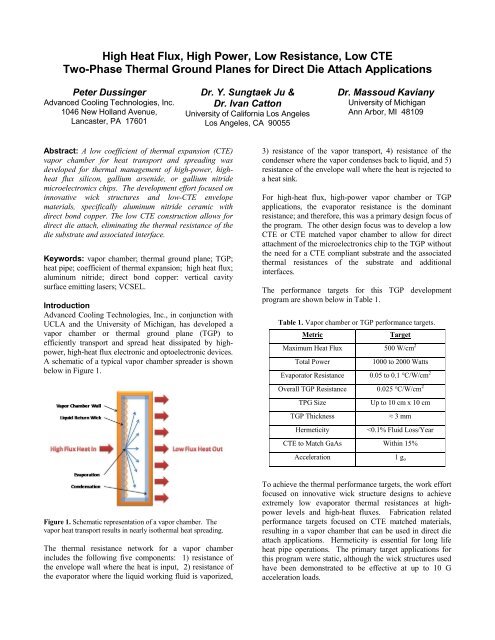
High Heat Flux, High Power, Low Resistance, Low CTE Two-Phase ...
High Heat Flux, High Power, Low Resistance, Low CTE Two-Phase ...
High Heat Flux, High Power, Low Resistance, Low CTE Two-Phase ...

You also want an ePaper? Increase the reach of your titles
YUMPU automatically turns print PDFs into web optimized ePapers that Google loves.
<strong>High</strong> <strong>Heat</strong> <strong>Flux</strong>, <strong>High</strong> <strong>Power</strong>, <strong>Low</strong> <strong>Resistance</strong>, <strong>Low</strong> <strong>CTE</strong><br />
<strong>Two</strong>-<strong>Phase</strong> Thermal Ground Planes for Direct Die Attach Applications<br />
Peter Dussinger<br />
Advanced Cooling Technologies, Inc.<br />
1046 New Holland Avenue,<br />
Lancaster, PA 17601<br />
Dr. Y. Sungtaek Ju &<br />
Dr. Ivan Catton<br />
University of California Los Angeles<br />
Los Angeles, CA 90055<br />
Dr. Massoud Kaviany<br />
University of Michigan<br />
Ann Arbor, MI 48109<br />
Abstract: A low coefficient of thermal expansion (<strong>CTE</strong>)<br />
vapor chamber for heat transport and spreading was<br />
developed for thermal management of high-power, highheat<br />
flux silicon, gallium arsenide, or gallium nitride<br />
microelectronics chips. The development effort focused on<br />
innovative wick structures and low-<strong>CTE</strong> envelope<br />
materials, specifically aluminum nitride ceramic with<br />
direct bond copper. The low <strong>CTE</strong> construction allows for<br />
direct die attach, eliminating the thermal resistance of the<br />
die substrate and associated interface.<br />
Keywords: vapor chamber; thermal ground plane; TGP;<br />
heat pipe; coefficient of thermal expansion; high heat flux;<br />
aluminum nitride; direct bond copper: vertical cavity<br />
surface emitting lasers; VCSEL.<br />
Introduction<br />
Advanced Cooling Technologies, Inc., in conjunction with<br />
UCLA and the University of Michigan, has developed a<br />
vapor chamber or thermal ground plane (TGP) to<br />
efficiently transport and spread heat dissipated by highpower,<br />
high-heat flux electronic and optoelectronic devices.<br />
A schematic of a typical vapor chamber spreader is shown<br />
below in Figure 1.<br />
3) resistance of the vapor transport, 4) resistance of the<br />
condenser where the vapor condenses back to liquid, and 5)<br />
resistance of the envelope wall where the heat is rejected to<br />
a heat sink.<br />
For high-heat flux, high-power vapor chamber or TGP<br />
applications, the evaporator resistance is the dominant<br />
resistance; and therefore, this was a primary design focus of<br />
the program. The other design focus was to develop a low<br />
<strong>CTE</strong> or <strong>CTE</strong> matched vapor chamber to allow for direct<br />
attachment of the microelectronics chip to the TGP without<br />
the need for a <strong>CTE</strong> compliant substrate and the associated<br />
thermal resistances of the substrate and additional<br />
interfaces.<br />
The performance targets for this TGP development<br />
program are shown below in Table 1.<br />
Table 1. Vapor chamber or TGP performance targets.<br />
Metric<br />
Target<br />
Maximum <strong>Heat</strong> <strong>Flux</strong> 500 W/cm 2<br />
Total <strong>Power</strong><br />
1000 to 2000 Watts<br />
Evaporator <strong>Resistance</strong> 0.05 to 0.1 °C/W/cm 2<br />
Overall TGP <strong>Resistance</strong> 0.025 °C/W/cm 2<br />
TPG Size<br />
TGP Thickness<br />
Hermeticity<br />
Up to 10 cm x 10 cm<br />
≈ 3 mm<br />
Wick Structure Design<br />
The purpose of the wick structure inside of the vapor<br />
chamber is to deliver the heat pipe working fluid to the heat<br />
input locations. At these locations, the heat causes the<br />
working fluid to evaporate or change phase from a liquid to<br />
a vapor. This vapor is at a slightly higher pressure than the<br />
vapor in the cooler areas of the vapor chamber (condenser<br />
region). This pressure difference causes the warmer vapor<br />
to flow to the condenser region, where it condenses back to<br />
a liquid, releasing the latent heat of vaporization. The wick<br />
structure absorbs this liquid and provides a flow path back<br />
to the evaporator. This cycle continues to transfer power<br />
from the evaporator regions of the vapor chamber to the<br />
condenser regions as long as there is a temperature<br />
difference between these two regions.<br />
The capillary pressure generated by the wick structure must<br />
be greater than the pressure drops of the vapor flow and the<br />
liquid return flow, otherwise the liquid flow will be<br />
insufficient to accept all of the input heat. When this<br />
happens, the wick structure "dries out" and the temperature<br />
of the electronic component will rise rapidly until failure.<br />
Therefore, in order to design a vapor chamber for highpower,<br />
high-heat fluxes, there must be enough vapor space<br />
cross-sectional area to allow the vapor to flow without<br />
significant resistance; and, there must be enough wick<br />
structure cross-sectional area to allow the liquid flow<br />
without significant resistance.<br />
For high-power and high-heat flux vapor chambers it<br />
would seem logical to have a very thick wick structure to<br />
deliver liquid at high flow rates to the evaporation sites.<br />
However, the large conduction thermal resistance of such a<br />
thick wick and the net reduction in the gap space available<br />
for vapor flows can lead to significant increase in the<br />
overall thermal resistance.<br />
So, while a thick liquid delivery wick is favorable for<br />
maximum critical heat flux (capillary limit), a thin wick<br />
structure is favorable for low evaporator thermal resistance.<br />
To simultaneously have high power and low thermal<br />
resistance, the ideal wick structure will have separate<br />
features for liquid delivery/vapor escape and for<br />
evaporation heat transfer. In this program, two liquid<br />
supply structures were developed: one for lateral liquid<br />
delivery (converging wick) and one for perpendicular<br />
liquid delivery (post array). Both designs have significant<br />
fractions of the evaporator area where the wick structure is<br />
very thin, practically a one or two particle thick layer of<br />
sintered copper powder. They also have a significant<br />
fraction of area that is devoted to liquid delivery, the lateral<br />
fingers for the converging wick designs and the posts for<br />
the post array designs.<br />
Photographs of representative converging wick and post<br />
array wicks are shown in Figures 2 and 3, respectively.<br />
Figure 2. Converging Wick Structure. Thick wick fingers deliver<br />
liquid to the thin wick sections between the fingers where<br />
evaporation takes place. Vapor escapes through the spaces<br />
between the fingers [3].<br />
Figure 3. Cylindrical Post Wick Structure. Tall sintered wick<br />
posts deliver liquid to the thin wick sections between the posts<br />
where evaporation takes place. Vapor escapes through the spaces<br />
between the posts [1-2].<br />
Prototype vapor chambers were built and tested with<br />
converging and post wick structures. The test fixture is<br />
shown in Figure 4 below.<br />
Phenolic Frame<br />
<strong>Heat</strong>er<br />
Vapor Chamber<br />
Liquid Cooled <strong>Heat</strong> Sinks<br />
Figure 4. <strong>High</strong> power, high heat flux test fixture. <strong>Heat</strong> input area<br />
is 1 cm 2 or 4 cm 2 (top center). <strong>Heat</strong> removal is through two watercooled<br />
heat sinks, 2 cm wide x 7.6cm long (bottom outside edges).<br />
A typical set of test data is plotted in Figure 5 below. The<br />
vapor chamber evaporator resistance is calculated from the<br />
temperature difference between a thermocouple inserted in<br />
a well drilled into the heat input pedestal and a<br />
thermocouple inserted into a well that protrudes into the<br />
vapor space divided by the electrical power input to the
copper heater block per square centimeter of heat input<br />
area. As seen in the plot, the evaporator thermal resistance<br />
decreases as the heat flux increases from 0 to about 400<br />
W/cm 2 . This decrease is commonly observed in sintered<br />
powder metal wicks and is often attributed to the<br />
evaporation location receding deeper into the wick<br />
structure with increasing heat flux. Above 400 W/cm 2 , the<br />
wick structure begins to dry out and the thermal resistance<br />
increases until it reaches a critical limiting heat flux around<br />
550 W/cm 2 .<br />
Tested with 0.2in x 3in x 5in Copper Vapor Chambers – 1cm 2 <strong>Heat</strong> Input Area<br />
Figure 5. Evaporator thermal resistance of converging and post<br />
wick structures as a function of heat flux.<br />
Both the converging and the post wick structures were<br />
successful in demonstrating excellent performance. <strong>Heat</strong><br />
fluxes up to 700 W/cm 2 were demonstrated with 1 cm 2 heat<br />
input and total power through a vapor chamber of nearly<br />
2000 W was demonstrated with a heat input size of 4 cm 2 .<br />
In both of these examples, the evaporator heat flux met or<br />
exceeded the target of 0.05 - 0.1 °C/W/cm 2 .<br />
<strong>Low</strong> <strong>CTE</strong> Materials and Construction<br />
Vapor chambers and TGPs for electronics cooling have<br />
typically been manufactured using copper and aluminum.<br />
These materials are very effective in making a high<br />
conductivity vapor chamber and have been used to spread<br />
heat from localized hot spots to larger area heat sinks<br />
(liquid and air cooled). In these cases, the microelectronic<br />
chips are typically thermally coupled to the TGP through<br />
interface materials like greases and pads. These greases<br />
and pads allow for slippage between the chip and the TGP<br />
as the device heats up and the copper or aluminum TGP<br />
expands more than the microelectronic chip.<br />
As the heat flux increases, greases and pads are no longer<br />
effective due to their relatively low thermal conductivity.<br />
Metallurgical bonds are far superior from a thermal<br />
resistance point of view; however, the differences in<br />
coefficient of thermal expansion (<strong>CTE</strong>) are too great and<br />
often lead to thermally induced fatigue failure of the joint.<br />
For example, silicon, gallium arsenide, and gallium nitride<br />
have <strong>CTE</strong>s of 2.6, 6.8, and 5.6 ppm/°C, respectively; while<br />
aluminum and copper have <strong>CTE</strong>s of 24 and 17 ppm/°C,<br />
respectively. To solve this issue, an intermediate substrate<br />
is often employed between the microelectronic chip and the<br />
TGP.<br />
Unfortunately, this is one of the most significant and<br />
unfavorable thermal resistances for a high-power, high-heat<br />
flux electronic chip. The substrate material is typically a<br />
poor conductor and the additional interface joint adds<br />
another thermal resistance.<br />
A thermally superior design would allow the<br />
microelectronic chip to be metallurgically bonded directly<br />
to the vapor chamber or TGP surface. To make that<br />
possible, the vapor chamber material of construction must<br />
be a <strong>CTE</strong> matched material to typical chip materials. In<br />
other words, the <strong>CTE</strong> for the TGP needs to be in the 3 to 6<br />
ppm/°C range.<br />
For this program, the material of choice for the envelope<br />
walls was Aluminum Nitride ceramic plates with Direct<br />
Bond Copper (DBC). Aluminum Nitride ceramic has a<br />
fairly high thermal conductivity (150 to 200 W/m-K)<br />
similar to aluminum and has a <strong>CTE</strong> of 4.5 ppm/°C. It is<br />
commercially available with thin layers of copper directly<br />
bonded to the surfaces.<br />
The thin layers of copper are necessary for three reasons.<br />
First, copper is compatible with water, the most common<br />
and effective vapor chamber working fluid for<br />
microelectronics cooling. Compatibility for a heat pipe or<br />
vapor chamber means that the working fluid and the<br />
envelope material will not react and generate noncondensable<br />
gases or corrode and leak. Copper/ water heat<br />
pipes have been used successfully for decades; therefore,<br />
utilizing this material system eliminates the need for<br />
extensive life testing that is required when new<br />
material/fluid combinations are proposed. The second<br />
reason for the copper layers allows for the use of<br />
conventional wick sintering and envelope sealing<br />
techniques. Again, using qualified sintering techniques and<br />
envelope sealing techniques eliminates the need for<br />
extensive life testing. And, for the third reason, the copper<br />
layer on the outside of the TGP allows for direct circuit<br />
etching onto the surface of the TGP.<br />
Manufacturing of the low <strong>CTE</strong> vapor chambers starts by<br />
sintering the copper powder wick structure directly onto<br />
one of the copper layers on an Aluminum Nitride ceramic<br />
envelope plate. A thin ring of copper plated Kovar, also a<br />
low <strong>CTE</strong> material (5.9 ppm/°C), was used to space two<br />
envelope plates apart creating the vapor space above the<br />
sintered wick. Braze materials with proven compatibility<br />
with water were used to join the envelope sheets to the<br />
Kovar ring, forming the hermetically leak tight vapor<br />
chamber envelope. A small diameter fill tube was also<br />
brazed into the Kovar ring to allow for fluid charging and<br />
evacuation prior to permanently sealing the TGP. The<br />
brazing temperatures are well above the soldering<br />
temperatures typically used to attach microelectronic chips<br />
to substrates; and therefore, the low-<strong>CTE</strong> TGP will not be
unfavorably affected by subsequent chip attach processes.<br />
The final <strong>CTE</strong> of the TGP devices was approximately 5.5<br />
ppm/°C.<br />
Figure 6 shows a variety of TGP sizes that were<br />
manufactured under this program. Larger sizes are only<br />
limited by material availability.<br />
Figure 7. TGP with etched electrical circuitry, gold plated with<br />
gold-tin solder pads ready for direct attach of 1 cm 2 VCSEL chips.<br />
A representative sample of the converging wick structure is shown<br />
in the lower right photograph.<br />
Figure 6. Various Vapor Chambers or Thermal Ground Planes<br />
from 3cm x 3cm to 10 cm x 10 cm.<br />
Potential Application<br />
Any high-power, high-heat flux microelectronic chip would<br />
likely benefit from the vapor chamber or thermal ground<br />
plane technology (e.g. high power amplifiers, IGBTs, and<br />
SCRs). For this DARPA sponsored program, the<br />
technology demonstration application was vertical cavity<br />
surface emitting lasers (VCSELs). VCSELs can be<br />
manufactured using typical semiconductor manufacturing<br />
techniques; and therefore, can be manufactured very cost<br />
effectively. In fact, nearly every computer mouse in use<br />
today has a VCSEL chip.<br />
<strong>High</strong>er power lasers for metal cutting, welding, and some<br />
directed energy weapons are for the most part driven by<br />
edge emitting lasers. While these edge emitting lasers are<br />
in use today, their geometry limits packing density and they<br />
typically require microchannel coolers that are susceptible<br />
to erosion and corrosion. The TGP and VCSEL<br />
combination allows for tiling of the VCSEL chips (tight<br />
packaging density) and the heat spreading of the TGP<br />
allows for conventional low velocity cold plates as the heat<br />
sink, eliminating the need for the costly high pressure<br />
pumps and fluid conditioning equipment associated with<br />
microchannel coolers.<br />
As a final demonstration of the TGP technology, several 10<br />
cm x 10 cm TGPs were fabricated and prepared for direct<br />
VCSEL attach. Figure 7 is a photograph of a TGP with a<br />
surface pattern etched circuit directly onto the surface. The<br />
TGP has been gold plated and pads of Gold-Tin solder<br />
have been deposited for direct attach of VCSEL chips. The<br />
high performance converging wick structure that is inside<br />
of the TGP is shown in the smaller inset photograph.<br />
Summary<br />
<strong>High</strong> heat-flux, high-power, low-resistance, low-<strong>CTE</strong> twophase<br />
thermal ground planes for direct die attach<br />
applications have been successfully developed.<br />
Demonstrated TGP performance and features include:<br />
• <strong>High</strong> <strong>Power</strong>: > 2000W with 4cm 2 <strong>Heat</strong> Input<br />
• <strong>High</strong> <strong>Heat</strong> <strong>Flux</strong>: > 700W/cm 2 with 1cm 2 <strong>Heat</strong> Input<br />
• <strong>Low</strong> Evaporator <strong>Resistance</strong>: 0.05 to 0.1 °C/W/cm 2<br />
• <strong>Low</strong> <strong>CTE</strong> -Aluminum Nitride Ceramic with Direct<br />
Bond Copper - Approximately 5.5 ppm/°C<br />
• Direct Die Attach - Direct Bond Copper Can be<br />
Etched for Electrical Circuitry, Gold Plated, Gold/Tin<br />
Deposited for Direct Solder Attach - Demonstrated<br />
on TGP Prototype<br />
Acknowledgements<br />
This material is based upon work supported by the Defense<br />
Advanced Research Project Agency (DARPA) and Space<br />
and Naval Warfare Systems Center (SPAWARS-YSCEN),<br />
San Diego, CA under Contract No. N66001-08-C-2007.<br />
The views, opinions, and/or findings contained in this<br />
article/presentation are those of the author/presenter and<br />
should not be interpreted as representing the official views<br />
or policies, either expressed or implied, of the DARPA or<br />
the Department of Defense.<br />
References<br />
1. Min, D.H. et al., Multi-artery heat pipe spreader,”<br />
International Journal of <strong>Heat</strong> and Mass Transfer,<br />
52:629-635, 2009.<br />
2. Hwang, G.S. et al., Multi-artery heat pipe spreader:<br />
Experiment,” International Journal of <strong>Heat</strong> and Mass<br />
Transfer, 53:2662-2670, 2010.<br />
3. Hwang, G.S. et al., “Multi-artery heat pipe spreader:<br />
Lateral liquid supply,” International Journal of <strong>Heat</strong><br />
and Mass Transfer, 54:2334-2340, 2011.