

FIN1018 3.3V LVDS 1-Bit High Speed ... - Fairchild Semiconductor
FIN1018 3.3V LVDS 1-Bit High Speed ... - Fairchild Semiconductor
FIN1018 3.3V LVDS 1-Bit High Speed ... - Fairchild Semiconductor

You also want an ePaper? Increase the reach of your titles
YUMPU automatically turns print PDFs into web optimized ePapers that Google loves.
March 2001<br />
Revised April 2002<br />
<strong>FIN1018</strong><br />
<strong>3.3V</strong> <strong>LVDS</strong> 1-<strong>Bit</strong> <strong>High</strong> <strong>Speed</strong> Differential Receiver<br />
General Description<br />
This single receiver is designed for high speed interconnects<br />
utilizing Low Voltage Differential Signaling (<strong>LVDS</strong>)<br />
technology. The receiver translates <strong>LVDS</strong> levels, with a typical<br />
differential input threshold of 100 mV, to LVTTL signal<br />
levels. <strong>LVDS</strong> provides low EMI at ultra low power dissipation<br />
even at high frequencies. This device is ideal for high<br />
speed transfer of clock or data.<br />
The <strong>FIN1018</strong> can be paired with its companion driver, the<br />
FIN1017, or with any other <strong>LVDS</strong> driver.<br />
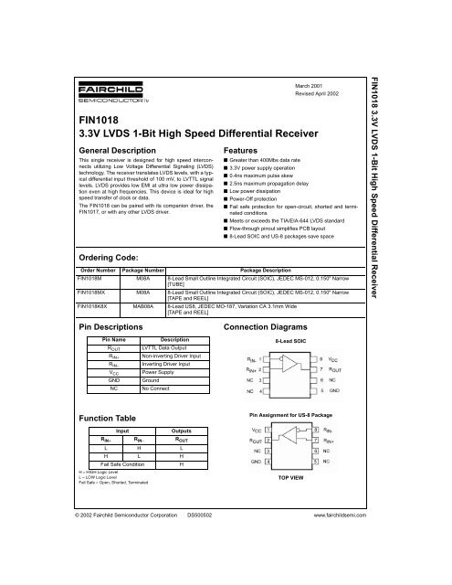
Ordering Code:<br />
Pin Descriptions<br />
Function Table<br />
H = HIGH Logic Level<br />
L = LOW Logic Level<br />
Fail Safe = Open, Shorted, Terminated<br />
Features<br />
■ Greater than 400Mbs data rate<br />
■ <strong>3.3V</strong> power supply operation<br />
■ 0.4ns maximum pulse skew<br />
■ 2.5ns maximum propagation delay<br />
■ Low power dissipation<br />
■ Power-Off protection<br />
■ Fail safe protection for open-circuit, shorted and terminated<br />
conditions<br />
■ Meets or exceeds the TIA/EIA-644 <strong>LVDS</strong> standard<br />
■ Flow-through pinout simplifies PCB layout<br />
■ 8-Lead SOIC and US-8 packages save space<br />
Order Number Package Number Package Description<br />
<strong>FIN1018</strong>M M08A 8-Lead Small Outline Integrated Circuit (SOIC), JEDEC MS-012, 0.150" Narrow<br />
[TUBE]<br />
<strong>FIN1018</strong>MX M08A 8-Lead Small Outline Integrated Circuit (SOIC), JEDEC MS-012, 0.150" Narrow<br />
[TAPE and REEL]<br />
<strong>FIN1018</strong>K8X MAB08A 8-Lead US8, JEDEC MO-187, Variation CA 3.1mm Wide<br />
[TAPE and REEL]<br />
Pin Name Description<br />
ROUT LVTTL Data Output<br />
RIN+ Non-inverting Driver Input<br />
RIN− Inverting Driver Input<br />
VCC Power Supply<br />
GND Ground<br />
NC No Connect<br />
Input Outputs<br />
RIN+ RIN− ROUT L H L<br />
H L H<br />
Fail Safe Condition H<br />
Connection Diagrams<br />
8-Lead SOIC<br />
Pin Assignment for US-8 Package<br />
TOP VIEW<br />
© 2002 <strong>Fairchild</strong> <strong>Semiconductor</strong> Corporation DS500502 www.fairchildsemi.com<br />
<strong>FIN1018</strong> <strong>3.3V</strong> <strong>LVDS</strong> 1-<strong>Bit</strong> <strong>High</strong> <strong>Speed</strong> Differential Receiver
<strong>FIN1018</strong><br />
Absolute Maximum Ratings(Note 1) Recommended Operating<br />
Conditions<br />
Supply Voltage (VCC ) −0.5V to +4.6V<br />
DC Input Voltage (RIN+ , RIN− ) −0.5V to +4.7V<br />
DC Output Voltage (DOUT) −0.5V to +6V<br />
DC Output Current (IO ) 16 mA<br />
Storage Temperature Range (TSTG ) −65°C to +150°C<br />
Max Junction Temperature (TJ) Lead Temperature (TL )<br />
150°C<br />
(Soldering, 10 seconds) 260°C<br />
ESD (Human Body Model) ≥ 6500V<br />
ESD (Bus Pins RIN− /RIN+ to GND) ≥ 9500V<br />
ESD (Machine Model) ≥ 300V<br />
DC Electrical Characteristics<br />
Over supply voltage and operating temperature ranges, unless otherwise specified<br />
www.fairchildsemi.com 2<br />
Note 1: The “Absolute Maximum Ratings”: are those values beyond which<br />
damage to the device may occur. The databook specifications should be<br />
met, without exception, to ensure that the system design is reliable over its<br />
power supply, temperature and output/input loading variables. <strong>Fairchild</strong><br />
does not recommend operation of circuits outside databook specification.<br />
Symbol Parameter Test Conditions<br />
Min Typ<br />
(Note 2)<br />
Max<br />
Units<br />
VTH Differential Input Threshold HIGH See Figure 1 and Table 1 100 mV<br />
VTL Differential Input Threshold LOW See Figure 1 and Table 1 −100 mV<br />
IIN Input Current VIN = 0V or VCC ±20 µA<br />
II(OFF) Power-OFF Input Current VCC = 0V, VIN = 0V or 3.6V ±20 µA<br />
VOH Output HIGH Voltage IOH = −100 µA VCC −0.2 V<br />
IOH = −8 mA 2.4 V<br />
VOL Output LOW Voltage IOH = 100 µA 0.2 V<br />
IOL = 8 mA 0.5 V<br />
VIK Input Clamp Voltage IIK = −18 mA −1.5 V<br />
ICC Power Supply Current Inputs Open, (RIN+ = 1V and RIN− = 1.4V),<br />
or (RIN+ = 1.4V and RIN− = 1V)<br />
7 mA<br />
CIN Input Capacitance 4 pF<br />
COUT Output Capacitance 6 pF<br />
Note 2: All typical values are at TA = 25°C and with VCC = <strong>3.3V</strong>.<br />
AC Electrical Characteristics<br />
Over supply voltage and operating temperature ranges, unless otherwise specified<br />
Supply Voltage (VCC ) 3.0V to 3.6V<br />
Input Voltage (VIN )<br />
Magnitude of Differential Voltage<br />
0 to VCC (|VID |) 100mV to VCC Common-mode Input Voltage (VIC ) 0.05V to 2.35V<br />
Operating Temperature (TA) −40°C to +85°C<br />
Symbol Parameter Test Conditions<br />
Min Typ<br />
(Note 3)<br />
Max<br />
Units<br />
tPLH Propagation Delay LOW-to-HIGH 0.9 2.5 ns<br />
tPHL Propagation Delay HIGH-to-LOW 0.9 2.5 ns<br />
tTLH Output Rise Time (20% to 80%) |VID | = 400 mV, CL = 10 pF 0.5 ns<br />
tTHL Output Fall Time (80% to 20%) See Figure 1 and Figure 2 0.5 ns<br />
tSK(P) Pulse Skew |tPLH - tPHL| 0.4 ns<br />
tSK(PP) Part-to-Part Skew (Note 4) 1.0 ns<br />
Note 3: All typical values are at TA = 25°C and with VCC = <strong>3.3V</strong>.<br />
Note 4: tSK(PP) is the magnitude of the difference in propagation delay times between any specified terminals of two devices switching in the same direction<br />
(either LOW-to-HIGH or HIGH-to-LOW) when both devices operate with the same supply voltage, same temperature, and have identical test circuits.
Note A: All input pulses have frequency = 10MHz, tR or tF = 1ns<br />
Note B: CL includes all probe and fixture capacitances<br />
FIGURE 1. Differential Receiver Voltage Definitions and Propagation Delay and Transition Time Test Circuit<br />
TABLE 1. Receiver Minimum and Maximum Input Threshold Test Voltages<br />
Applied Voltages (V)<br />
Resulting Differential<br />
Input Voltage (mV)<br />
Resulting Common Mode<br />
Input Voltage (V)<br />
VIA VIB VID VIC 1.25 1.15 100 1.2<br />
1.15 1.25 −100 1.2<br />
2.4 2.3 100 2.35<br />
2.3 2.4 −100 2.35<br />
0.1 0 100 0.05<br />
0 0.1 −100 0.05<br />
1.5 0.9 600 1.2<br />
0.9 1.5 −600 1.2<br />
2.4 1.8 600 2.1<br />
1.8 2.4 −600 2.1<br />
0.6 0 600 0.3<br />
0 0.6 −600 0.3<br />
FIGURE 2. <strong>LVDS</strong> Input to LVTTL Output AC Waveforms<br />
3 www.fairchildsemi.com<br />
<strong>FIN1018</strong>
<strong>FIN1018</strong><br />
DC / AC Typical Performance Curves<br />
FIGURE 3. Output <strong>High</strong> Voltage vs.<br />
Power Supply Voltage<br />
FIGURE 5. Output Short Circuit Current vs.<br />
Power Supply Voltage<br />
FIGURE 7. Power Supply Current vs.<br />
Ambient Temperature<br />
www.fairchildsemi.com 4<br />
FIGURE 4. Output Low Voltage vs.<br />
Power Supply Voltage<br />
FIGURE 6. Power Supply Current vs.<br />
Frequency<br />
FIGURE 8. Differential Propagation Delay<br />
Power Supply Voltage
DC / AC Typical Performance Curves (Continued)<br />
FIGURE 9. Differential Propagation Delay vs.<br />
Ambient Temperature<br />
FIGURE 11. Differential Skew vs.<br />
Ambient Temperature<br />
FIGURE 13. Differential Propagation Delay vs.<br />
Common-Mode Voltage<br />
FIGURE 10. Differential Skew vs.<br />
Power Supply Voltage<br />
FIGURE 12. Differential Propagation Delay vs.<br />
Differential Input Voltage<br />
FIGURE 14. Transition Time vs.<br />
Power Supply Voltage<br />
5 www.fairchildsemi.com<br />
<strong>FIN1018</strong>
<strong>FIN1018</strong><br />
DC / AC Typical Performance Curves (Continued)<br />
FIGURE 15. Transition Time vs.<br />
Ambient Temperature<br />
FIGURE 17. Differential Propagation Delay vs.<br />
Load<br />
FIGURE 19. Transition Time vs.<br />
Load<br />
www.fairchildsemi.com 6<br />
FIGURE 16. Differential Propagation Delay vs.<br />
Load<br />
FIGURE 18. Transition Time vs.<br />
Load<br />
FIGURE 20. Power Supply Current vs.<br />
Power Supply Voltage
Physical Dimensions inches (millimeters) unless otherwise noted<br />
8-Lead Small Outline Integrated Circuit (SOIC), JEDEC MS-012, 0.150" Narrow<br />
Package Number M08A<br />
7 www.fairchildsemi.com<br />
<strong>FIN1018</strong>
<strong>FIN1018</strong> <strong>3.3V</strong> <strong>LVDS</strong> 1-<strong>Bit</strong> <strong>High</strong> <strong>Speed</strong> Differential Receiver<br />
Physical Dimensions inches (millimeters) unless otherwise noted (Continued)<br />
8-Lead US8, JEDEC MO-187, Variation CA 3.1mm Wide<br />
Package Number MAB08A<br />
<strong>Fairchild</strong> does not assume any responsibility for use of any circuitry described, no circuit patent licenses are implied and<br />
<strong>Fairchild</strong> reserves the right at any time without notice to change said circuitry and specifications.<br />
LIFE SUPPORT POLICY<br />
FAIRCHILD’S PRODUCTS ARE NOT AUTHORIZED FOR USE AS CRITICAL COMPONENTS IN LIFE SUPPORT<br />
DEVICES OR SYSTEMS WITHOUT THE EXPRESS WRITTEN APPROVAL OF THE PRESIDENT OF FAIRCHILD<br />
SEMICONDUCTOR CORPORATION. As used herein:<br />
1. Life support devices or systems are devices or systems<br />
which, (a) are intended for surgical implant into the<br />
body, or (b) support or sustain life, and (c) whose failure<br />
to perform when properly used in accordance with<br />
instructions for use provided in the labeling, can be reasonably<br />
expected to result in a significant injury to the<br />
user.<br />
www.fairchildsemi.com 8<br />
2. A critical component in any component of a life support<br />
device or system whose failure to perform can be reasonably<br />
expected to cause the failure of the life support<br />
device or system, or to affect its safety or effectiveness.<br />
www.fairchildsemi.com


