

ADG787: 2.5 Ω CMOS Low Power Dual 2:1 Mux/Demux USB 1.1 ...
ADG787: 2.5 Ω CMOS Low Power Dual 2:1 Mux/Demux USB 1.1 ...
ADG787: 2.5 Ω CMOS Low Power Dual 2:1 Mux/Demux USB 1.1 ...

You also want an ePaper? Increase the reach of your titles
YUMPU automatically turns print PDFs into web optimized ePapers that Google loves.
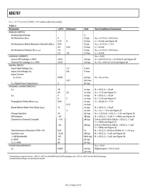
<strong>ADG787</strong><br />
VDD = 2.7 V to 3.6 V, GND = 0 V, unless otherwise noted.<br />
Table 2.<br />
Parameter +25°C B Version 1 Unit Test Conditions/Comments<br />
ANALOG SWITCH<br />
Analog Signal Range V<br />
On Resistance (RON) 4 <strong>Ω</strong> typ VDD = 2.7 V, VS = 0 V to VDD<br />
5.75 6 <strong>Ω</strong> max IS = 10 mA; see Figure 28<br />
On Resistance Match Between Channels (ΔRON) 0.07 <strong>Ω</strong> typ VDD = 2.7 V, VS = 1.5 V<br />
0.3 0.35 <strong>Ω</strong> max IS = 10 mA<br />
On Resistance Flatness (RFLAT (ON)) 1.6 <strong>Ω</strong> typ VDD = 2.7 V, VS = 0 V to VDD<br />
2.3 2.6 <strong>Ω</strong> max IS = 10 mA<br />
LEAKAGE CURRENTS VDD = 3.6 V<br />
Source Off Leakage, IS (OFF) ±0.01 nA typ VS = 0.6 V/3.3 V, VD = 3.3 V/0.6 V; see Figure 29<br />
Channel On Leakage, ID, IS (ON) ±0.01 nA typ VS = VD = 0.6 V or 3.3 V; see Figure 30<br />
DIGITAL INPUTS<br />
Input High Voltage, VINH 1.3 V min<br />
Input <strong>Low</strong> Voltage, VINL 0.8 V max<br />
Input Current<br />
IINL or IINH 0.005 μA typ VIN = VINL or VINH<br />
±0.1 μA max<br />
CIN, Digital Input Capacitance 2 pF typ<br />
DYNAMIC CHARACTERISTICS 2<br />
tON 18 ns typ RL = 50 <strong>Ω</strong>, CL = 35 pF<br />
30 35 ns max VS = 1.5 V; see Figure 31<br />
tOFF 4 ns typ RL = 50 <strong>Ω</strong>, CL = 35 pF<br />
6 7 ns max VS = 1.5 V; see Figure 31<br />
Propagation Delay Skew, tSKEW 0.04 ns typ CL = 50 pF; VS = 1.5 V<br />
0.12 ns max<br />
Break-Before-Make Time Delay (tBBM) 15 ns typ RL = 50 <strong>Ω</strong>, CL = 35 pF<br />
5 ns min VS1 = VS2 = 1.5 V; see Figure 32<br />
Charge Injection 10 pC typ VD = 1.25 V, RS = 0 <strong>Ω</strong>, CL = 1 nF; see Figure 33<br />
Off Isolation −63 dB typ RL = 50 <strong>Ω</strong>, CL = 5 pF, f = 1 MHz; see Figure 34<br />
Channel-to-Channel Crosstalk −110 dB typ S1A to S2A/S1B to S2B; RL = 50 <strong>Ω</strong>, CL = 5 pF,<br />
f = 1 MHz; see Figure 37<br />
−63 dB typ S1A to S1B/S2A to S2B; RL = 50 <strong>Ω</strong>, CL = 5 pF,<br />
f = 1 MHz; see Figure 35<br />
Total Harmonic Distortion (THD + N) 0.07 % RL = 32 <strong>Ω</strong>, f = 20 Hz to 20 kHz, VS = 1.5 V p-p<br />
Insertion Loss −0.24 dB typ RL = 50 <strong>Ω</strong>, CL = 5 pF; see Figure 36<br />
−3 dB Bandwidth 145 MHz typ RL = 50 <strong>Ω</strong>, CL = 5 pF; see Figure 36<br />
CS (OFF) 16 pF typ<br />
CD, CS (ON) 40 pF typ<br />
POWER REQUIREMENTS VDD = 3.6 V<br />
IDD 0.005 μA typ Digital inputs = 0 V or 3.6 V<br />
1 μA max<br />
1 Temperature range: B version: −40°C to +85°C for the MSOP and LFCSP packages, and −25°C to +85°C for the WLCSP package.<br />
2 Guaranteed by design, not production tested.<br />
Rev. A | Page 4 of 16


