

ADG787: 2.5 Ω CMOS Low Power Dual 2:1 Mux/Demux USB 1.1 ...
ADG787: 2.5 Ω CMOS Low Power Dual 2:1 Mux/Demux USB 1.1 ...
ADG787: 2.5 Ω CMOS Low Power Dual 2:1 Mux/Demux USB 1.1 ...

You also want an ePaper? Increase the reach of your titles
YUMPU automatically turns print PDFs into web optimized ePapers that Google loves.
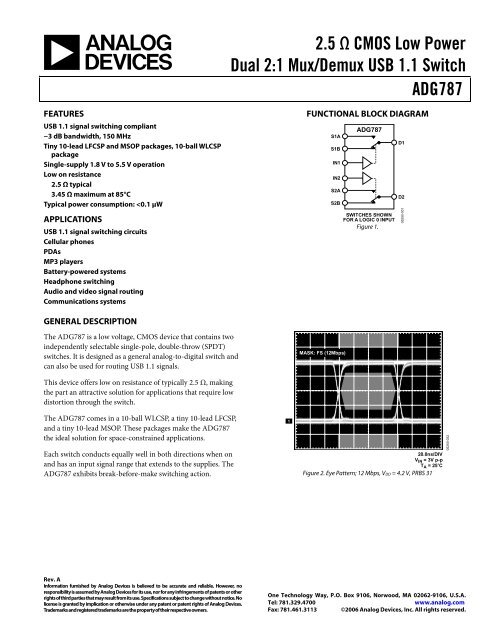
FEATURES<br />
<strong>USB</strong> <strong>1.1</strong> signal switching compliant<br />
−3 dB bandwidth, 150 MHz<br />
Tiny 10-lead LFCSP and MSOP packages, 10-ball WLCSP<br />
package<br />
Single-supply 1.8 V to 5.5 V operation<br />
<strong>Low</strong> on resistance<br />
<strong>2.5</strong> <strong>Ω</strong> typical<br />
3.45 <strong>Ω</strong> maximum at 85°C<br />
Typical power consumption:
<strong>ADG787</strong><br />
TABLE OF CONTENTS<br />
Features .............................................................................................. 1<br />
Applications....................................................................................... 1<br />
Functional Block Diagram .............................................................. 1<br />
General Description ......................................................................... 1<br />
Specifications..................................................................................... 3<br />
Absolute Maximum Ratings............................................................ 5<br />
ESD Caution.................................................................................. 5<br />
REVISION HISTORY<br />
5/06—Rev. 0 to Rev. A<br />
Updated Formatting...........................................................Universal<br />
Changes to Table 1............................................................................ 3<br />
Changes to Table 3............................................................................ 5<br />
Changes to Ordering Guide .......................................................... 15<br />
1/05—Revision 0: Initial Version<br />
Rev. A | Page 2 of 16<br />
Pin Configurations and Function Descriptions ............................6<br />
Truth Table .....................................................................................6<br />
Typical Performance Characteristics ..............................................7<br />
Test Circuits ................................................................................ 11<br />
Terminology.................................................................................... 13<br />
Outline Dimensions ....................................................................... 14<br />
Ordering Guide .......................................................................... 15
SPECIFICATIONS<br />
VDD = 4.2 V to 5.5 V, GND = 0 V, unless otherwise noted.<br />
Rev. A | Page 3 of 16<br />
<strong>ADG787</strong><br />
Table 1.<br />
Parameter +25°C B Version 1 Unit Test Conditions/Comments<br />
ANALOG SWITCH<br />
Analog Signal Range 0 to VDD V<br />
On Resistance (RON) <strong>2.5</strong> <strong>Ω</strong> typ VDD = 4.2 V, VS = 0 V to VDD, IS = 10 mA<br />
3 3.45 <strong>Ω</strong> max See Figure 28<br />
On Resistance Match Between Channels (ΔRON) 0.02 <strong>Ω</strong> typ VDD = 4.2 V, VS = 3.5 V, IS = 10 mA<br />
0.1 <strong>Ω</strong> max<br />
On Resistance Flatness (RFLAT (ON)) 0.65 <strong>Ω</strong> typ VDD = 4.2 V, VS = 0 V to VDD<br />
0.8 0.95 <strong>Ω</strong> max IS = 10 mA<br />
LEAKAGE CURRENTS VDD = 5.5 V<br />
Source Off Leakage, IS (OFF) ±0.05 nA typ VS = 1 V/4.5 V, VD = 4.5 V/1 V; see Figure 29<br />
Channel On Leakage, ID, IS (ON) ±0.05 nA typ VS = VD = 1 V or 4.5 V; see Figure 30<br />
DIGITAL INPUTS<br />
Input High Voltage, VINH 2.0 V min<br />
Input <strong>Low</strong> Voltage, VINL 0.8 V max<br />
Input Current<br />
IINL or IINH 0.005 μA typ VIN = VINL or VINH<br />
±0.1 μA max<br />
CIN, Digital Input Capacitance <strong>2.5</strong> pF typ<br />
DYNAMIC CHARACTERISTICS 2<br />
tON 13 ns typ RL = 50 <strong>Ω</strong>, CL = 35 pF<br />
19 22 ns max VS = 3 V; see Figure 31<br />
tOFF 3 ns typ RL = 50 <strong>Ω</strong>, CL = 35 pF<br />
5 6 ns max VS = 3 V; see Figure 31<br />
Propagation Delay Skew, tSKEW 0.06 ns typ CL = 50 pF; VS = 3 V<br />
0.15 ns max<br />
Break-Before-Make Time Delay (tBBM) 10 ns typ RL = 50 <strong>Ω</strong>, CL = 35 pF<br />
5 ns min VS1 = VS2 = 3 V; see Figure 32<br />
Charge Injection 14 pC typ VD = 1 V, RS = 0 <strong>Ω</strong>, CL = 1 nF; see Figure 33<br />
Off Isolation −63 dB typ RL = 50 <strong>Ω</strong>, CL = 5 pF, f = 1 MHz; see Figure 34<br />
Channel-to-Channel Crosstalk −110 dB typ S1A to S2A/S1B to S2B; RL = 50 <strong>Ω</strong>, CL = 5 pF,<br />
f = 1 MHz; see Figure 37<br />
−63 dB typ S1A to S1B/S2A to S2B; RL = 50 <strong>Ω</strong>, CL = 5 pF,<br />
f = 1 MHz; see Figure 36<br />
Total Harmonic Distortion (THD + N) 0.03 % RL = 32 <strong>Ω</strong>, f = 20 Hz to 20 kHz, VS = 2 V p-p<br />
Insertion Loss −0.2 dB typ RL = 50 <strong>Ω</strong>, CL = 5 pF; see Figure 36<br />
−3 dB Bandwidth 145 MHz typ RL = 50 <strong>Ω</strong>, CL = 5 pF; see Figure 36<br />
CS (OFF) 16 pF typ<br />
CD, CS (ON) 40 pF typ<br />
POWER REQUIREMENTS VDD = 5.5 V<br />
IDD 0.005 μA typ Digital inputs = 0 V or 5.5 V<br />
1 μA max<br />
1 Temperature ranges: B version: −40°C to +85°C for the MSOP and LFCSP packages, and −25°C to +85°C for the WLCSP package.<br />
2 Guaranteed by design, not production tested.
<strong>ADG787</strong><br />
VDD = 2.7 V to 3.6 V, GND = 0 V, unless otherwise noted.<br />
Table 2.<br />
Parameter +25°C B Version 1 Unit Test Conditions/Comments<br />
ANALOG SWITCH<br />
Analog Signal Range V<br />
On Resistance (RON) 4 <strong>Ω</strong> typ VDD = 2.7 V, VS = 0 V to VDD<br />
5.75 6 <strong>Ω</strong> max IS = 10 mA; see Figure 28<br />
On Resistance Match Between Channels (ΔRON) 0.07 <strong>Ω</strong> typ VDD = 2.7 V, VS = 1.5 V<br />
0.3 0.35 <strong>Ω</strong> max IS = 10 mA<br />
On Resistance Flatness (RFLAT (ON)) 1.6 <strong>Ω</strong> typ VDD = 2.7 V, VS = 0 V to VDD<br />
2.3 2.6 <strong>Ω</strong> max IS = 10 mA<br />
LEAKAGE CURRENTS VDD = 3.6 V<br />
Source Off Leakage, IS (OFF) ±0.01 nA typ VS = 0.6 V/3.3 V, VD = 3.3 V/0.6 V; see Figure 29<br />
Channel On Leakage, ID, IS (ON) ±0.01 nA typ VS = VD = 0.6 V or 3.3 V; see Figure 30<br />
DIGITAL INPUTS<br />
Input High Voltage, VINH 1.3 V min<br />
Input <strong>Low</strong> Voltage, VINL 0.8 V max<br />
Input Current<br />
IINL or IINH 0.005 μA typ VIN = VINL or VINH<br />
±0.1 μA max<br />
CIN, Digital Input Capacitance 2 pF typ<br />
DYNAMIC CHARACTERISTICS 2<br />
tON 18 ns typ RL = 50 <strong>Ω</strong>, CL = 35 pF<br />
30 35 ns max VS = 1.5 V; see Figure 31<br />
tOFF 4 ns typ RL = 50 <strong>Ω</strong>, CL = 35 pF<br />
6 7 ns max VS = 1.5 V; see Figure 31<br />
Propagation Delay Skew, tSKEW 0.04 ns typ CL = 50 pF; VS = 1.5 V<br />
0.12 ns max<br />
Break-Before-Make Time Delay (tBBM) 15 ns typ RL = 50 <strong>Ω</strong>, CL = 35 pF<br />
5 ns min VS1 = VS2 = 1.5 V; see Figure 32<br />
Charge Injection 10 pC typ VD = 1.25 V, RS = 0 <strong>Ω</strong>, CL = 1 nF; see Figure 33<br />
Off Isolation −63 dB typ RL = 50 <strong>Ω</strong>, CL = 5 pF, f = 1 MHz; see Figure 34<br />
Channel-to-Channel Crosstalk −110 dB typ S1A to S2A/S1B to S2B; RL = 50 <strong>Ω</strong>, CL = 5 pF,<br />
f = 1 MHz; see Figure 37<br />
−63 dB typ S1A to S1B/S2A to S2B; RL = 50 <strong>Ω</strong>, CL = 5 pF,<br />
f = 1 MHz; see Figure 35<br />
Total Harmonic Distortion (THD + N) 0.07 % RL = 32 <strong>Ω</strong>, f = 20 Hz to 20 kHz, VS = 1.5 V p-p<br />
Insertion Loss −0.24 dB typ RL = 50 <strong>Ω</strong>, CL = 5 pF; see Figure 36<br />
−3 dB Bandwidth 145 MHz typ RL = 50 <strong>Ω</strong>, CL = 5 pF; see Figure 36<br />
CS (OFF) 16 pF typ<br />
CD, CS (ON) 40 pF typ<br />
POWER REQUIREMENTS VDD = 3.6 V<br />
IDD 0.005 μA typ Digital inputs = 0 V or 3.6 V<br />
1 μA max<br />
1 Temperature range: B version: −40°C to +85°C for the MSOP and LFCSP packages, and −25°C to +85°C for the WLCSP package.<br />
2 Guaranteed by design, not production tested.<br />
Rev. A | Page 4 of 16
ABSOLUTE MAXIMUM RATINGS<br />
TA = 25°C, unless otherwise noted.<br />
Table 3.<br />
Parameter Rating<br />
VDD to GND −0.3 V to +6 V<br />
Analog Inputs 1 , Digital Inputs −0.3 V to VDD + 0.3 V or<br />
30 mA (whichever<br />
occurs first)<br />
Peak Current, S or D<br />
5 V Operation 300 mA<br />
3.3 V Operation 200 mA (pulsed at 1 ms,<br />
10% duty cycle max)<br />
Continuous Current, S or D<br />
5 V Operation 100 mA<br />
3.3 V Operation 80 mA<br />
Operating Temperature Range<br />
Extended Industrial (B Version)<br />
MSOP and LFCSP packages −40°C to +85°C<br />
Industrial (B version)<br />
WLCSP package −25°C to +85°C<br />
Storage Temperature Range −65°C to +150°C<br />
Junction Temperature 150°C<br />
WLCSP Package (4-Layer Board)<br />
θJA Thermal Impedance 120°C/W<br />
LFCSP Package (4-Layer Board)<br />
θJA Thermal Impedance 61°C/W<br />
MSOP Package (4-Layer Board)<br />
θJA Thermal Impedance 142°C/W<br />
θJC Thermal Impedance 43.7°C/W<br />
Lead-Free Temperature Soldering<br />
IR Reflow, Peak Temperature<br />
Peak Temperature 260(+0/−5)°C<br />
Time at Peak Temperature 10 sec to 40 sec<br />
1 Overvoltages at the IN, S, or D pins are clamped by internal diodes. Current<br />
should be limited to the maximum ratings given.<br />
Rev. A | Page 5 of 16<br />
<strong>ADG787</strong><br />
Stresses above those listed under Absolute Maximum Ratings<br />
may cause permanent damage to the device. This is a stress<br />
rating only; functional operation of the device at these or any<br />
other conditions above those listed in the operational sections<br />
of this specification is not implied. Exposure to absolute<br />
maximum rating conditions for extended periods may affect<br />
device reliability.<br />
Only one absolute maximum rating may be applied at any one<br />
time.<br />
ESD CAUTION<br />
ESD (electrostatic discharge) sensitive device. Electrostatic charges as high as 4000 V readily accumulate<br />
on the human body and test equipment and can discharge without detection. Although this product features<br />
proprietary ESD protection circuitry, permanent damage may occur on devices subjected to high energy<br />
electrostatic discharges. Therefore, proper ESD precautions are recommended to avoid performance<br />
degradation or loss of functionality.
<strong>ADG787</strong><br />
PIN CONFIGURATIONS AND FUNCTION DESCRIPTIONS<br />
V DD 1<br />
S1A 2<br />
D1 3<br />
IN1 4<br />
S1B 5<br />
<strong>ADG787</strong><br />
TOP VIEW<br />
(Not to Scale)<br />
10 S2A<br />
9 D2<br />
8 IN2<br />
7 S2B<br />
6 GND<br />
Figure 3. 10-Lead LFCSP and 10-lead MSOP Pin Configuration<br />
Table 4. 10-Lead LFCSP/MSOP Pin Function Descriptions<br />
Pin<br />
No. Mnemonic Description<br />
1 VDD Most Positive <strong>Power</strong> Supply Potential.<br />
2 S1A Source Terminal. May be an input or<br />
output.<br />
3 D1 Drain Terminal. May be an input or<br />
output.<br />
4 IN1 Logic Control Input.<br />
5 S1B Source Terminal. May be an input or<br />
output.<br />
6 GND Ground (0 V) Reference.<br />
7 S2B Source Terminal. May be an input or<br />
output.<br />
8 IN2 Logic Control Input.<br />
9 D2 Drain Terminal. May be an input or<br />
output.<br />
10 S2A Source Terminal. May be an input or<br />
output.<br />
05250-002<br />
Rev. A | Page 6 of 16<br />
a b c<br />
1<br />
S1B GND S2B<br />
2<br />
IN1 IN2<br />
3<br />
D1 D2<br />
4<br />
S1A VDD S2A<br />
TOP VIEW<br />
(BALLS AT THE BOTTOM)<br />
Figure 4. 10-Ball WLCSP Pin Configuration<br />
Table 5. 10-Lead WLCSP Pin Function Descriptions<br />
Ball<br />
Location Mnemonic Description<br />
1a S1B Source Terminal. May be an input or<br />
output.<br />
1b GND Ground (0 V) Reference.<br />
1c S2B Source Terminal. May be an input or<br />
output.<br />
2a IN1 Source Terminal. May be an input or<br />
output.<br />
2c IN2 Logic Control Input.<br />
3a D1 Drain Terminal. May be an input or<br />
output.<br />
3c D2 Drain Terminal. May be an input or<br />
output.<br />
4a S1A Logic Control Input.<br />
4b VDD Most Positive <strong>Power</strong> Supply Potential.<br />
4c S2A Source Terminal. May be an input or<br />
output.<br />
TRUTH TABLE<br />
Table 6.<br />
Logic (IN1/IN2) Switch 1A/2A Switch 1B/2B<br />
0 Off On<br />
1 On Off<br />
05250-003
TYPICAL PERFORMANCE CHARACTERISTICS<br />
ON RESISTANCE (W)<br />
ON RESISTANCE (W)<br />
ON RESISTANCE (W)<br />
3.0<br />
<strong>2.5</strong><br />
2.0<br />
1.5<br />
1.0<br />
0.5<br />
5.0<br />
4.5<br />
4.0<br />
3.5<br />
3.0<br />
<strong>2.5</strong><br />
2.0<br />
1.5<br />
1.0<br />
0.5<br />
V DD = 4.5V<br />
V DD = 4.2V<br />
V DD = 5V V DD = 5.5V<br />
0<br />
0 1 2 3 4 5<br />
SIGNAL RANGE<br />
T A = 25°C<br />
I DS = 10mA<br />
Figure 5. On Resistance vs. VD (VS), VDD = 4.2 V to 5.5 V<br />
T A = 25°C<br />
I DS = 10mA<br />
V DD = 3.3V<br />
V DD = 3V<br />
V DD = 2.7V<br />
V DD = 3.6V<br />
0<br />
0 0.5 1.0 1.5 2.0 <strong>2.5</strong> 3.0 3.5 4.0<br />
SIGNAL RANGE<br />
3.0<br />
<strong>2.5</strong><br />
2.0<br />
1.5<br />
1.0<br />
0.5<br />
Figure 6. On Resistance vs. VD (VS), VDD = 2.7 V to 3.6 V<br />
T A = +85°C<br />
T A = +25°C<br />
T A = –40°C<br />
0<br />
0 0.5 1.0 1.5 2.0 <strong>2.5</strong> 3.0 3.5 4.0 4.5 5.0<br />
SIGNAL RANGE<br />
V DD = 5V<br />
I DS = 10mA<br />
Figure 7. On Resistance vs. VD (VS) for Different Temperatures, VDD = 5 V<br />
05250-004<br />
05250-005<br />
05250-006<br />
Rev. A | Page 7 of 16<br />
ON RESISTANCE (W)<br />
3.5<br />
3.0<br />
<strong>2.5</strong><br />
2.0<br />
1.5<br />
1.0<br />
0.5<br />
T A = +85°C<br />
T A = +25°C<br />
T A = –40°C<br />
0<br />
0 0.5 1.0 1.5 2.0 <strong>2.5</strong> 3.0 3.5 4.0<br />
SIGNAL RANGE<br />
V DD = 4.2V<br />
I DS = 10mA<br />
<strong>ADG787</strong><br />
Figure 8. On Resistance vs. VD (VS) for Different Temperatures, VDD = 4.2 V<br />
ON RESISTANCE (W)<br />
5.0<br />
4.5<br />
4.0<br />
3.5<br />
3.0<br />
<strong>2.5</strong><br />
2.0<br />
1.5<br />
1.0<br />
0.5<br />
T A = +25°C<br />
T A = +85°C<br />
T A = –40°C<br />
V DD = 3V<br />
I DS = 10mA<br />
0<br />
0 0.5 1.0 1.5<br />
SIGNAL RANGE<br />
2.0 <strong>2.5</strong> 3.0<br />
Figure 9. On Resistance vs. VD (VS) for Different Temperatures, VDD = 3 V<br />
CURRENT (nA)<br />
2.0<br />
1.5<br />
1.0<br />
0.5<br />
0<br />
–0.5<br />
–1.0<br />
–1.5<br />
I S , I D (ON)<br />
I S (OFF)<br />
–2.0<br />
0 10 20 30 40 50 60 70 80<br />
TEMPERATURE (°C)<br />
Figure 10. Leakage Current vs. Temperature, VDD = 5.5 V<br />
05250-007<br />
05250-008<br />
05250-040
<strong>ADG787</strong><br />
Q INJ (pC)<br />
CURRENT (nA)<br />
LOGIC THRESHOLD POINT (V)<br />
25<br />
20<br />
15<br />
10<br />
5<br />
2.0<br />
1.5<br />
1.0<br />
0.5<br />
0<br />
–0.5<br />
–1.0<br />
–1.5<br />
I S (OFF)<br />
I S , I D (ON)<br />
–2.0<br />
0 10 20 30 40 50 60 70 80<br />
TEMPERATURE (°C)<br />
2.0<br />
1.8<br />
1.6<br />
1.4<br />
1.2<br />
1.0<br />
0.8<br />
0.6<br />
0.4<br />
0.2<br />
Figure 11. Leakage Current vs. Temperature, VDD = 3.3 V<br />
V IN RISING V IN FALLING<br />
0<br />
1.5 2.0 <strong>2.5</strong> 3.0 3.5 4.0 4.5 5.0 5.5<br />
SUPPLY VOLTAGE VDD (V)<br />
Figure 12. Threshold Voltage vs. Supply<br />
T A = 25°C V DD = 5V<br />
V DD = 3V<br />
0<br />
0 0.5 1.0 1.5 2.0 <strong>2.5</strong> 3.0 3.5 4.0 4.5 5.0<br />
V D (V)<br />
Figure 13. Charge Injection vs. Source Voltage<br />
05250-012<br />
05250-041<br />
05250-011<br />
Rev. A | Page 8 of 16<br />
TIME (ns)<br />
ATTENUATION (dB)<br />
ATTENUATION (dB)<br />
30<br />
25<br />
20<br />
15<br />
10<br />
5<br />
T A = 25°C<br />
V DD = 3V<br />
T ON<br />
V DD = 5V<br />
T OFF<br />
V DD = 3V<br />
VDD = 5V<br />
0<br />
–40 –20 0 20 40 60 80<br />
0<br />
–1<br />
–2<br />
–3<br />
–4<br />
–5<br />
–6<br />
–7<br />
TEMPERATURE (°C)<br />
Figure 14. tON/tOFF Time vs. Temperature<br />
V DD = 3V/4.2V/5V<br />
T A = 25°C<br />
–8<br />
100 1k 10k 100k 1M 10M 100M 1G<br />
FREQUENCY (Hz)<br />
0<br />
–20<br />
–40<br />
–60<br />
–80<br />
–100<br />
V DD = 3V/4.2V/5V<br />
T A = 25°C<br />
Figure 15. Bandwidth<br />
–120<br />
100 1k 10k 100k 1M 10M 100M 1G<br />
FREQUENCY (Hz)<br />
Figure 16. Off Isolation vs. Frequency<br />
05250-013<br />
05250-014<br />
05250-015
ATTENUATION (dB)<br />
PSRR (dB)<br />
THD+N (%)<br />
0<br />
–20<br />
–40<br />
–60<br />
–80<br />
–100<br />
V DD = 3V/4.2V/5V<br />
T A = 25°C<br />
S1A TO S1B<br />
–120<br />
100 1k 10k 100k 1M 10M 100M 1G<br />
0<br />
–20<br />
–40<br />
–60<br />
–80<br />
–100<br />
FREQUENCY (Hz)<br />
Figure 17. Crosstalk vs. Frequency<br />
V DD = 3V/4.2V/5V<br />
T A = 25°C<br />
NO SUPPLY DECOUPLING<br />
S1A TO S2A<br />
–120<br />
100 1k 10k 100k 1M 10M 100M 1G<br />
0.10<br />
0.09<br />
0.08<br />
0.07<br />
0.06<br />
0.05<br />
0.04<br />
0.03<br />
0.02<br />
0.01<br />
FREQUENCY (Hz)<br />
Figure 18. AC <strong>Power</strong> Supply Rejection Ratio (PSRR)<br />
V DD = 3V, V S = 2V p-p<br />
V DD = 5V, V S = 2V p-p<br />
0<br />
10 100 1k<br />
FREQUENCY (Hz)<br />
10k<br />
100k<br />
Figure 19. Total Harmonic Distortion + Noise<br />
05250-030<br />
05250-031<br />
05250-043<br />
Rev. A | Page 9 of 16<br />
DELAY (ns)<br />
DELAY (ns)<br />
MISMATCH (ns)<br />
3.0<br />
<strong>2.5</strong><br />
2.0<br />
1.5<br />
1.0<br />
0.5<br />
INPUT RISE/FALL TIME = 15ns<br />
T A = 25°C<br />
RISE DELAY<br />
0<br />
2.7 3.2 3.7 4.2 4.7 5.2<br />
2.0<br />
1.8<br />
1.6<br />
1.4<br />
1.2<br />
1.0<br />
0.8<br />
0.6<br />
0.4<br />
0.2<br />
SUPPLY VOLTAGE (V)<br />
FALL DELAY<br />
Figure 20. Rise/Fall Time Delay vs. Supply Voltage<br />
INPUT RISE/FALL TIME = 15ns<br />
V DD = 4.2V<br />
RISE DELAY<br />
FALL DELAY<br />
<strong>ADG787</strong><br />
0<br />
–40 –15 10 35 60 85<br />
TEMPERATURE (°C)<br />
2.0<br />
1.5<br />
1.0<br />
0.5<br />
Figure 21. Rise/Fall Time Delay vs. Temperature<br />
INPUT RISE/FALL TIME = 15ns<br />
T A = 25°C<br />
0<br />
<strong>2.5</strong> 3.0 3.5 4.0 4.5 5.0 5.5<br />
SUPPLY (V)<br />
Figure 22. Rise-Time-to-Fall-Time Mismatch vs. Supply Voltage<br />
05250-044<br />
05250-045<br />
05250-046
<strong>ADG787</strong><br />
MISMATCH (ns)<br />
T PROP SKEW (ps)<br />
T SKEW (ps)<br />
1.2<br />
1.0<br />
0.8<br />
0.6<br />
0.4<br />
0.2<br />
INPUT RISE/FALL TIME = 15ns<br />
V DD = 4.2V<br />
0<br />
–40 –15 10 35 60 85<br />
TEMPERATURE (°C)<br />
Figure 23. Rise-Time-to-Fall-Time Mismatch vs. Temperature<br />
300<br />
250<br />
200<br />
150<br />
100<br />
50<br />
INPUT RISE/FALL TIME = 15ns<br />
T A = 25°C<br />
0<br />
<strong>2.5</strong> 3.0 3.5 4.0 4.5 5.0 5.5<br />
SUPPLY (V)<br />
Figure 24. Propagation Delay Skew (tSKEW) vs. Supply Voltage<br />
200<br />
180<br />
160<br />
140<br />
120<br />
100<br />
80<br />
60<br />
40<br />
20<br />
INPUT RISE/FALL TIME = 15ns<br />
V DD = 4.2V<br />
0<br />
–40 –15 10 35 60 85<br />
TEMPERATURE (°C)<br />
Figure 25. Propagation Delay Skew (tSKEW) vs. Temperature<br />
05250-047<br />
05250-048<br />
05250-049<br />
Rev. A | Page 10 of 16<br />
1<br />
MASK: FS (12Mbps)<br />
20.0ns/DIV<br />
<strong>2.5</strong>GS/s 400ps/pt<br />
Figure 26. Eye Pattern, 12 Mbps, VDD = 4.2 V, TA = 85°C, PRBS 31<br />
1<br />
MASK: FS (12Mbps)<br />
20.0ns/DIV<br />
<strong>2.5</strong>GS/s 400ps/pt<br />
Figure 27. Eye Pattern, 12 Mbps, VDD = 4.2 V, TA = −40°C, PRBS 31<br />
05250-033<br />
05250-034
TEST CIRCUITS<br />
V S<br />
I DS<br />
V1<br />
S D<br />
R ON = V1/I DS<br />
Figure 28. On Resistance<br />
V S<br />
V S<br />
IN<br />
V S<br />
IN<br />
0.1μF<br />
0.1μF<br />
S1B<br />
S1A<br />
V DD<br />
VDD S1B<br />
S1A<br />
IN<br />
GND<br />
GND<br />
D<br />
V DD<br />
V DD<br />
D<br />
V DD<br />
GND<br />
D<br />
S1B<br />
S1A<br />
05250-016<br />
R L<br />
50<strong>Ω</strong><br />
R L<br />
50<strong>Ω</strong><br />
V OUT<br />
C L<br />
35pF<br />
V IN<br />
V OUT<br />
Figure 31. Switching Times, tON, tOFF<br />
V OUT<br />
C L<br />
35pF<br />
V IN<br />
V OUT<br />
Rev. A | Page 11 of 16<br />
0V<br />
80%<br />
V S<br />
IS (OFF) ID (OFF)<br />
S D<br />
A A<br />
Figure 29. Off Leakage<br />
NC<br />
S D<br />
ID (ON)<br />
A<br />
50% 50%<br />
t ON<br />
t BBM<br />
Figure 32. Break-Before-Make Time Delay, tBBM<br />
1nF<br />
NC<br />
V OUT<br />
V IN<br />
V OUT<br />
SW ON<br />
ΔV OUT<br />
Figure 33. Charge Injection<br />
Figure 30. On Leakage<br />
90% 90%<br />
50% 50%<br />
SW OFF<br />
Q INJ = CL ⋅ ΔV OUT<br />
80%<br />
t OFF<br />
t BBM<br />
05250-019<br />
05250-021<br />
05250-020<br />
V D<br />
V D<br />
05250-017<br />
05250-018<br />
<strong>ADG787</strong>
<strong>ADG787</strong><br />
NC<br />
V OUT<br />
VDD 0.1μF<br />
V DD<br />
S1B S1A<br />
D<br />
GND<br />
OFF ISOLATION = 20 LOG<br />
R L<br />
50<strong>Ω</strong><br />
50<strong>Ω</strong><br />
V S<br />
50<strong>Ω</strong><br />
V OUT<br />
VS<br />
Figure 34. Off Isolation<br />
0.1μF<br />
S1A<br />
S1B<br />
V DD<br />
V DD<br />
GND<br />
CHANNEL-TO-CHANNEL CROSSTALK = 20 LOG V OUT<br />
VS<br />
NETWORK<br />
ANALYZER<br />
50<strong>Ω</strong><br />
V S<br />
VOUT RL 50<strong>Ω</strong><br />
Figure 35. Channel-to-Channel Crosstalk (S1A to S1B)<br />
D<br />
R L<br />
50<strong>Ω</strong><br />
05250-023<br />
05250-022<br />
Rev. A | Page 12 of 16<br />
V OUT<br />
VDD 0.1μF<br />
S1B<br />
V DD<br />
GND<br />
S1A<br />
D<br />
NETWORK<br />
ANALYZER<br />
50<strong>Ω</strong><br />
V S<br />
VOUT RL 50<strong>Ω</strong><br />
VOUT WITH SWITCH<br />
INSERTION LOSS = 20 LOG<br />
VOUT WITHOUT SWITCH<br />
NETWORK<br />
ANALYZER<br />
50<strong>Ω</strong><br />
50<strong>Ω</strong><br />
V S<br />
Figure 36. Bandwidth<br />
S2A<br />
S2B<br />
S1A<br />
S1B<br />
CHANNEL-TO-CHANNEL CROSSTALK = 20 LOG V OUT<br />
VS<br />
Figure 37. Channel-to-Channel Crosstalk (S1A to S2A)<br />
D2<br />
D1<br />
NC<br />
05250-024<br />
NC<br />
50<strong>Ω</strong><br />
05250-025
TERMINOLOGY<br />
IDD<br />
Positive supply current.<br />
VD (VS)<br />
Analog voltage on Terminal D and Terminal S.<br />
RON<br />
Ohmic resistance between D and S.<br />
RFLAT (ON)<br />
Flatness is defined as the difference between the maximum and<br />
minimum value of on resistance as measured.<br />
ΔRON<br />
On resistance match between any two channels.<br />
IS (OFF)<br />
Source leakage current with the switch off.<br />
ID (OFF)<br />
Drain leakage current with the switch off.<br />
ID, IS (ON)<br />
Channel leakage current with the switch on.<br />
VINL<br />
Maximum input voltage for Logic 0.<br />
VINH<br />
Minimum input voltage for Logic 1.<br />
IINL (IINH)<br />
Input current of the digital input.<br />
CS (OFF)<br />
Off switch source capacitance. Measured with reference to<br />
ground.<br />
CD (OFF)<br />
Off switch drain capacitance. Measured with reference to<br />
ground.<br />
CD, CS (ON)<br />
On switch capacitance. Measured with reference to ground.<br />
CIN<br />
Digital input capacitance.<br />
tON<br />
Delay time between the 50% and the 90% points of the digital<br />
input and switch on condition.<br />
Rev. A | Page 13 of 16<br />
<strong>ADG787</strong><br />
tOFF<br />
Delay time between the 50% and the 90% points of the digital<br />
input and switch off condition.<br />
tBBM<br />
On or off time measured between the 80% points of both<br />
switches when switching from one to another.<br />
Charge Injection<br />
A measure of the glitch impulse transferred from the digital<br />
input to the analog output during on-off switching.<br />
Off Isolation<br />
A measure of unwanted signal coupling through an off switch.<br />
Crosstalk<br />
A measure of unwanted signal that is coupled from one channel<br />
to another as a result of parasitic capacitance.<br />
−3 dB Bandwidth<br />
The frequency at which the output is attenuated by 3 dB.<br />
On Response<br />
The frequency response of the on switch.<br />
Insertion Loss<br />
The loss due to the on resistance of the switch.<br />
THD + N<br />
The ratio of the harmonic amplitudes plus noise of a signal, to<br />
the fundamental.<br />
TSKEW<br />
The measure of the variation in propagation delay between each<br />
channel.<br />
Rise Time Delay<br />
The rise time of a signal is a measure of the time for the signal<br />
to rise from 10% of the ON level to 90% of the ON level. Rise<br />
time delay is the difference between the rise time, measured at<br />
the input, and the rise time, measured at the output.<br />
Fall Time Delay<br />
The fall time of a signal is a measure of the time for the signal to<br />
fall from 90% of the ON level to 10% of the ON level. Fall time<br />
delay is the difference between the fall time, measured at the<br />
input, and the fall time, measured at the output.<br />
Rise-Time-to-Fall-Time Mismatch<br />
This is the absolute value between the variation in the fall time<br />
and the rise time, measured at the output.
<strong>ADG787</strong><br />
OUTLINE DIMENSIONS<br />
1.50<br />
BCS SQ<br />
0.80<br />
0.75<br />
0.70<br />
SEATING<br />
PLANE<br />
0.95<br />
0.85<br />
0.75<br />
3.10<br />
3.00<br />
2.90<br />
3.10<br />
3.00<br />
2.90<br />
PIN 1<br />
0.15<br />
0.05<br />
INDEX<br />
AREA<br />
3.00<br />
BSC SQ<br />
TOP VIEW<br />
SIDE VIEW<br />
0.30<br />
0.23<br />
0.18<br />
0.80 MAX<br />
0.55 TYP<br />
0.50<br />
BSC<br />
0.50<br />
0.40<br />
0.30<br />
Rev. A | Page 14 of 16<br />
10<br />
6<br />
0.05 MAX<br />
0.02 NOM<br />
0.20 REF<br />
EXPOSED<br />
PAD<br />
(BOTTOM VIEW)<br />
1.74<br />
1.64<br />
1.49<br />
PIN 1<br />
INDICATOR<br />
Figure 38. 10-Lead Lead Frame Chip Scale Package [LFCSP_WD]<br />
3 mm × 3 mm Body, Very, Very Thin, <strong>Dual</strong> Lead (CP-10-9)<br />
Dimensions shown in millimeters<br />
10 6<br />
1<br />
0.33<br />
0.17<br />
5<br />
0.50 BSC<br />
COPLANARITY<br />
0.10<br />
5.15<br />
4.90<br />
4.65<br />
<strong>1.1</strong>0 MAX<br />
SEATING<br />
PLANE<br />
0.23<br />
0.08<br />
8°<br />
0°<br />
COMPLIANT TO JEDEC STANDARDS MO-187-BA<br />
Figure 39. 10-Lead Mini Small Outline Package [MSOP]<br />
(RM-10)<br />
Dimensions shown in millimeters<br />
1<br />
5<br />
2.48<br />
2.38<br />
2.23<br />
0.80<br />
0.60<br />
0.40
BALL 1<br />
IDENTIFIER<br />
1.56<br />
1.50<br />
1.44<br />
TOP VIEW<br />
(BALL SIDE DOWN)<br />
2.06<br />
2.00<br />
1.94<br />
Rev. A | Page 15 of 16<br />
0.63<br />
0.57<br />
0.51<br />
SEATING<br />
PLANE<br />
0.26<br />
0.22<br />
0.18<br />
0.36<br />
0.32<br />
0.28<br />
0.50 BSC<br />
BALL PITCH<br />
0.11<br />
0.09<br />
0.07<br />
Figure 40. 10-Ball Wafer Level Chip Scale Package [WLCSP]<br />
(CB-10)<br />
Dimensions shown in millimeters<br />
C<br />
B<br />
BOTTOM<br />
VIEW<br />
(BALL SIDE UP)<br />
A<br />
1<br />
2<br />
3<br />
4<br />
111105-0<br />
<strong>ADG787</strong><br />
ORDERING GUIDE<br />
Model Temperature Range Package Description Package Option Branding 1<br />
<strong>ADG787</strong>BRMZ 2 –40°C to +85°C 10-Lead Mini Small Outline Package (MSOP) RM-10 SM1<br />
<strong>ADG787</strong>BRMZ-500RL7 2 –40°C to +85°C 10-Lead Mini Small Outline Package (MSOP) RM-10 SM1<br />
<strong>ADG787</strong>BRMZ-REEL 2 –40°C to +85°C 10-Lead Mini Small Outline Package (MSOP) RM-10 SM1<br />
<strong>ADG787</strong>BCBZ-500RL7 2 –25°C to +85°C 10-Ball Wafer Level Chip Scale Package (WLCSP) CB-10 S04<br />
<strong>ADG787</strong>BCBZ-REEL 2 –25°C to +85°C 10-Ball Wafer Level Chip Scale Package (WLCSP) CB-10 S04<br />
<strong>ADG787</strong>BCPZ-500RL7 2 –40°C to +85°C 10-Lead Lead Frame Chip Scale Package (LFCSP_WD) CP-10-9 SM1<br />
<strong>ADG787</strong>BCPZ-REEL 2 –40°C to +85°C 10-Lead Lead Frame Chip Scale Package (LFCSP_WD) CP-10-9 SM1<br />
1 Due to space constraints, branding on this package is limited to three characters.<br />
2 Z = Pb-free part.
<strong>ADG787</strong><br />
NOTES<br />
©2006 Analog Devices, Inc. All rights reserved. Trademarks and<br />
registered trademarks are the property of their respective owners.<br />
D05250-0-5/06(A)<br />
Rev. A | Page 16 of 16


