

ADG772 CMOS Low Power Dual 2:1 Mux/Demux USB 2.0 (480 ...
ADG772 CMOS Low Power Dual 2:1 Mux/Demux USB 2.0 (480 ...
ADG772 CMOS Low Power Dual 2:1 Mux/Demux USB 2.0 (480 ...

You also want an ePaper? Increase the reach of your titles
YUMPU automatically turns print PDFs into web optimized ePapers that Google loves.
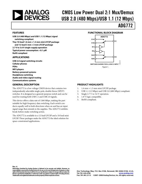
FEATURES<br />
<strong>USB</strong> <strong>2.0</strong> (<strong>480</strong> Mbps) and <strong>USB</strong> 1.1 (12 Mbps) signal<br />
switching compliant<br />
Tiny 10-lead 1.6 mm × 1.3 mm mini LFCSP package<br />
and 12-lead 3 mm × 3 mm LFCSP package<br />
2.7 V to 3.6 V single-supply operation<br />
Typical power consumption:
<strong>ADG772</strong><br />
TABLE OF CONTENTS<br />
Features .............................................................................................. 1<br />
Applications ....................................................................................... 1<br />
Functional Block Diagram .............................................................. 1<br />
General Description ......................................................................... 1<br />
Product Highlights ........................................................................... 1<br />
Revision History ............................................................................... 2<br />
Specifications ..................................................................................... 3<br />
Absolute Maximum Ratings ............................................................ 4<br />
REVISION HISTORY<br />
6/08—Rev. 0 to Rev. A<br />
Changes to Product Highlights ....................................................... 1<br />
Changes to Input High Voltage, VINH, Parameter ......................... 3<br />
8/07—Revision 0: Initial Version<br />
Rev. A | Page 2 of 12<br />
ESD Caution...................................................................................4<br />
Pin Configuration and Function Descriptions ..............................5<br />
Truth Table .....................................................................................5<br />
Typical Performance Characteristics ..............................................6<br />
Test Circuits ........................................................................................9<br />
Terminology .................................................................................... 11<br />
Outline Dimensions ....................................................................... 12<br />
Ordering Guide .......................................................................... 12
SPECIFICATIONS<br />
VDD = 2.7 V to 3.6 V, GND = 0 V, unless otherwise noted.<br />
Rev. A | Page 3 of 12<br />
<strong>ADG772</strong><br />
Table 1.<br />
Parameter +25°C −40°C to +85°C Unit Test Conditions/Comments<br />
ANALOG SWITCH<br />
Analog Signal Range 0 V to VDD V<br />
On-Resistance (RON) 6.7 Ω typ VDD = 2.7 V, VS = 0 V to VDD, IDS = 10 mA; see Figure 21<br />
8.8 Ω max<br />
On-Resistance Match 0.04 Ω typ VDD = 2.7 V, VS = 1.5 V, IDS = 10 mA<br />
Between Channels (∆RON) 0.2 Ω max<br />
On Resistance Flatness (RFLAT (ON)) 3.3 Ω typ VDD = 2.7 V, VS = 0 V to VDD, IDS = 10 mA<br />
3.6 Ω max<br />
LEAKAGE CURRENTS VDD = 3.6 V<br />
Source Off Leakage IS (Off) ±0.2 nA typ VS = 0.6 V/3.3 V, VD = 3.3 V/0.6 V; see Figure 22<br />
Channel On Leakage ID, IS (On) ±0.2 nA typ VS = VD = 0.6 V or 3.3 V; see Figure 23<br />
DIGITAL INPUTS<br />
Input High Voltage, VINH 1.35 V min<br />
Input <strong>Low</strong> Voltage, VINL 0.8 V max<br />
Input Current, IINL or IINH 0.005 μA typ VIN = VINL or VINH<br />
±0.1 μA max VIN = VINL or VINH<br />
Digital Input Capacitance, CIN 2 pF typ<br />
DYNAMIC CHARACTERISTICS 1<br />
tON 9 ns typ RL = 50 Ω, CL = 35 pF<br />
12.5 13.5 ns max VS = 2 V; see Figure 24<br />
tOFF 6 ns typ RL = 50 Ω, CL = 35 pF<br />
9.5 10 ns max VS = 2 V; see Figure 24<br />
Propagation Delay 250 ps typ RL = 50 Ω, CL = 35 pF<br />
Propagation Delay Skew, tSKEW 20 ps typ RL = 50 Ω, CL = 35 pF<br />
Break-Before-Make Time Delay (tBBM) 5 ns typ RL = 50 Ω, CL = 35 pF<br />
3.4 2.9 ns min VS1 = VS2 = 2 V; see Figure 25<br />
Charge Injection 0.5 pC typ VD = 1.25 V, RS = 0 Ω, CL = 1 nF; see Figure 26<br />
Off Isolation 73 dB typ RL = 50 Ω, CL = 5 pF, f = 1 MHz; see Figure 27<br />
Channel-to-Channel Crosstalk −90 dB typ S1A to S2A/S1B to S2B; RL = 50 Ω, CL = 5 pF,<br />
f = 1 MHz; see Figure 28<br />
−80 dB typ S1A to S1B/S2A to S2B; RL = 50 Ω, CL = 5 pF,<br />
f = 1 MHz; see Figure 29<br />
−3 dB Bandwidth 630 MHz typ RL = 50 Ω, CL = 5 pF; see Figure 30<br />
Data Rate 1260 Mbps typ RL = 50 Ω, CL = 5 pF; see Figure 30<br />
CS (Off) 2.4 pF typ<br />
CD, CS (On) 6.9 pF typ<br />
POWER REQUIREMENTS VDD = 3.6 V<br />
IDD 0.006 μA typ Digital inputs = 0 V or 3.6 V<br />
1 μA max<br />
1 Guaranteed by design, not subject to production test.
<strong>ADG772</strong><br />
ABSOLUTE MAXIMUM RATINGS<br />
TA = 25°C, unless otherwise noted.<br />
Table 2.<br />
Parameter Rating<br />
VDD to GND −0.3 V to +4.6 V<br />
Analog Inputs, 1 Digital Inputs −0.3 V to VDD + 0.3 V or<br />
10 mA, whichever occurs first<br />
Peak Current, Pin S1A, Pin S2A, 100 mA (pulsed at 1 ms, 10%<br />
Pin D1, or Pin D2<br />
duty cycle max)<br />
Continuous Current, Pin S1A,<br />
Pin S2A, Pin D1, or Pin D2<br />
30 mA<br />
Operating Temperature<br />
Industrial Range (B Version)<br />
−40°C to +85°C<br />
Storage Temperature Range −65°C to +150°C<br />
Junction Temperature<br />
θJA Thermal Impedance<br />
(4-Layer Board)<br />
150°C<br />
10-Lead Mini LFCSP 131.6°C/W<br />
12-Lead LFCSP<br />
Pb-Free Temperature,<br />
Soldering, IR Reflow<br />
61°C/W<br />
Peak Temperature 260(+0/−5)°C<br />
Time at Peak Temperature 10 sec to 40 sec<br />
1 Overvoltages at the IN1, IN2, S1A, S2A, D1, or D2 pin are clamped by internal<br />
diodes. Current should be limited to the maximum ratings given.<br />
Rev. A | Page 4 of 12<br />
Stresses above those listed under Absolute Maximum Ratings<br />
may cause permanent damage to the device. This is a stress<br />
rating only; functional operation of the device at these or any<br />
other conditions above those indicated in the operational<br />
section of this specification is not implied. Exposure to absolute<br />
maximum rating conditions for extended periods may affect<br />
device reliability.<br />
Only one absolute maximum rating can be applied at any<br />
one time.<br />
ESD CAUTION
PIN CONFIGURATION AND FUNCTION DESCRIPTIONS<br />
D1 2<br />
S1B 3<br />
S1A<br />
1<br />
4<br />
IN1<br />
GND<br />
10<br />
<strong>ADG772</strong><br />
TOP VIEW<br />
(Not to Scale)<br />
5<br />
IN2<br />
S2A<br />
6<br />
9<br />
VDD<br />
8 D2<br />
7 S2B<br />
Figure 2. 10-Lead Mini LFCSP Pin Configuration<br />
006692-002<br />
Rev. A | Page 5 of 12<br />
D1 1<br />
S1B 2<br />
NC 3<br />
12 S1A<br />
11 GND<br />
PIN 1<br />
INDICATOR<br />
<strong>ADG772</strong><br />
TOP VIEW<br />
(Not to Scale)<br />
IN1 4<br />
IN2 5<br />
VDD 6<br />
9 D2<br />
8 S2B<br />
7 NC<br />
NC = NO CONNECT<br />
Figure 3. 12-Lead LFCSP Pin Configuration<br />
10 S2A<br />
06692-003<br />
<strong>ADG772</strong><br />
Table 3. Pin Function Descriptions<br />
Pin No.<br />
10-Lead Mini LFCSP 12-Lead LFCSP Mnemonic Description<br />
1 12 S1A Source Terminal. Can be an input or an output.<br />
2 1 D1 Drain Terminal. Can be an input or an output.<br />
3 2 S1B Source Terminal. Can be an input or an output.<br />
4 4 IN1 Logic Control Input. This pin controls Switch S1A and Switch S1B to D1.<br />
5 5 IN2 Login Control Input. This pin controls Switch S2A and Switch S2B to D2.<br />
6 6 VDD Most Positive <strong>Power</strong> Supply Potential.<br />
7 8 S2B Source Terminal. Can be an input or an output.<br />
8 9 D2 Drain Terminal. Can be an input or an output.<br />
9 10 S2A Source Terminal. Can be an input or an output.<br />
10 11 GND Ground (0 V) Reference.<br />
N/A 3, 7 NC No Connect.<br />
TRUTH TABLE<br />
Table 4.<br />
Logic (IN1 or IN2) Switch A (S1A or S2A) Switch B (S1B or S2B)<br />
0 Off On<br />
1 On Off
<strong>ADG772</strong><br />
TYPICAL PERFORMANCE CHARACTERISTICS<br />
ON RESISTANCE (Ω)<br />
ON RESISTANCE (Ω)<br />
ON RESISTANCE (Ω)<br />
7<br />
6<br />
5<br />
4<br />
3<br />
2<br />
1<br />
0<br />
10<br />
9<br />
8<br />
7<br />
6<br />
5<br />
4<br />
3<br />
2<br />
1<br />
0<br />
30<br />
25<br />
20<br />
15<br />
10<br />
5<br />
0<br />
T A = 25°C<br />
V DD = 3.0V<br />
V DD = 3.3V<br />
V DD = 3.6V<br />
0 0.5 1.0 1.5 <strong>2.0</strong> 2.5 3.0 3.5 4.0<br />
V D , V S (V) 06692-024<br />
Figure 4. On Resistance vs. VD, VS; VDD = 3.3 V ± 0.3 V<br />
T A = 25°C<br />
VDD = 2.3V<br />
VDD = 2.5V<br />
V DD = 2.7V<br />
06692-023<br />
0 0.5 1.0 1.5 <strong>2.0</strong> 2.5 3.0 3.5<br />
VD , VS (V)<br />
Figure 5. On Resistance vs. VD, VS; VDD = 2.5 V ± 0.2 V<br />
T A = 25°C<br />
V DD = 1.65V<br />
V DD = 1.8V<br />
V DD = 1.95V<br />
0 0.2 0.4 0.6 0.8 1.0 1.2 1.4 1.6 1.8 <strong>2.0</strong><br />
V D , V S (V) 06692-022<br />
Figure 6. On Resistance vs. VD, VS; VDD = 1.8 V ± 0.15 V<br />
Rev. A | Page 6 of 12<br />
ON RESISTANCE (Ω)<br />
7<br />
6<br />
5<br />
4<br />
3<br />
2<br />
1<br />
0<br />
T A = +85°C<br />
T A = –40°C<br />
T A = +25°C<br />
V DD = 3.3V<br />
0 0.5 1.0 1.5 <strong>2.0</strong> 2.5 3.0 3.5<br />
V D , V S (V) 06692-027<br />
Figure 7. On Resistance vs. VD, VS for Different Temperatures; VDD = 3.3 V<br />
ON RESISTANCE (Ω)<br />
8<br />
7<br />
6<br />
5<br />
4<br />
3<br />
2<br />
1<br />
0<br />
V DD = 2.7V<br />
T A = +85°C<br />
T A = +25°C<br />
T A = –40°C<br />
0 0.5 1.0 1.5 <strong>2.0</strong> 2.5 3.0<br />
V D , V S (V) 06692-026<br />
Figure 8. On Resistance vs. VD, VS for Different Temperatures; VDD = 2.7 V<br />
ON RESISTANCE (Ω)<br />
25<br />
20<br />
15<br />
10<br />
5<br />
0<br />
V DD = 1.8V<br />
T A = –40°C<br />
T A = +25°C<br />
T A = +85°C<br />
0 0.2 0.4 0.6 0.8 1.0 1.2 1.4 1.6 1.8 <strong>2.0</strong><br />
V D , V S (V) 06692-025<br />
Figure 9. On Resistance vs. VD, VS for Different Temperatures; VDD = 1.8 V
CURRENT (nA)<br />
CURRENT (nA)<br />
CURRENT (nA)<br />
2.5<br />
<strong>2.0</strong><br />
1.5<br />
1.0<br />
0.5<br />
0<br />
V DD = 3.3V<br />
I D , I S (ON)++<br />
I D , I S (OFF)+–<br />
06692-028<br />
–0.5<br />
–1.0<br />
0 10 20<br />
ID , IS (ON)––<br />
ID , IS (OFF)–+<br />
30 40 50 60 70 80 90<br />
TEMPERATURE (°C)<br />
0.9<br />
0.8<br />
0.7<br />
0.6<br />
0.5<br />
0.4<br />
0.3<br />
0.2<br />
0.1<br />
Figure 10. Leakage Current vs. Temperature; VDD = 3.3 V<br />
V DD = 2.5V<br />
I D , I S (OFF)+–<br />
I D , I S (ON)++<br />
I D , I S (ON)––<br />
06692-029<br />
0<br />
ID , IS (OFF)–+<br />
–0.1<br />
0 10 20 30 40 50 60 70 80 90<br />
TEMPERATURE (°C)<br />
Figure 11. Leakage Current vs. Temperature; VDD = 2.5 V<br />
0.8<br />
0.7<br />
0.6<br />
0.5<br />
0.4<br />
0.3<br />
0.2<br />
0.1<br />
0<br />
–0.1<br />
V DD = 1.8V<br />
I D , I S (ON)––<br />
I D , I S (ON)++<br />
I D , I S (OFF)+–<br />
06692-030<br />
0 10 20<br />
ID , IS (OFF)–+<br />
30 40 50 60 70 80 90<br />
TEMPERATURE (°C)<br />
Figure 12. Leakage Current vs. Temperature; VDD = 1.8 V<br />
Rev. A | Page 7 of 12<br />
Q INJ (pC)<br />
TIME (ns)<br />
INSERTION LOSS (dB)<br />
<strong>2.0</strong><br />
1.5<br />
1.0<br />
0.5<br />
0<br />
–0.5<br />
–1<br />
12<br />
10<br />
8<br />
6<br />
4<br />
2<br />
T A = 25°C<br />
V CC = 1.8V<br />
V CC = 2.5V<br />
V CC = 3.3V<br />
<strong>ADG772</strong><br />
0 0.5 1.0 1.5 <strong>2.0</strong> 2.5 3.0 3.5<br />
V S (V)<br />
0<br />
–40 –20<br />
0<br />
–2<br />
–4<br />
–6<br />
–8<br />
–10<br />
–12<br />
–14<br />
–16<br />
–18<br />
Figure 13. Charge Injection vs. Source Voltage<br />
t ON (1.8V)<br />
t OFF (1.8V)<br />
t OFF (3.3V)<br />
t ON (3.3V)<br />
t ON (2.7V)<br />
0 20 40 60 80 85<br />
TEMPERATURE (°C)<br />
t OFF (2.7V)<br />
Figure 14. tON/tOFF Times vs. Temperature<br />
T A = 25°C<br />
V DD = 3.3V, 2.5V, 1.8V<br />
1 10 100 1000<br />
FREQUENCY (MHz)<br />
Figure 15. Bandwidth<br />
06692-018<br />
06692-019<br />
06692-014
<strong>ADG772</strong><br />
ATTENUATION (dB)<br />
CROSSTALK (dB)<br />
PSRR (dB)<br />
0<br />
–10<br />
–20<br />
–30<br />
–40<br />
–50<br />
–60<br />
–70<br />
–80<br />
–90<br />
–100<br />
T A = 25°C<br />
V DD = 3.3V, 2.5V, 1.8V<br />
1 10 100 1000<br />
FREQUENCY (MHz)<br />
Figure 16. Off Isolation vs. Frequency<br />
0<br />
TA = 25°C<br />
–10 VDD = 3.3V, 2.5V, 1.8V<br />
–20<br />
–30<br />
–40<br />
–50<br />
–60<br />
–70<br />
–80<br />
–90<br />
–100<br />
0<br />
TA = 25°C<br />
VDD = 3.3V<br />
–20<br />
–40<br />
–60<br />
–80<br />
–100<br />
–120<br />
S1A to S1B<br />
S1A to S2A<br />
1 10 100 1000<br />
FREQUENCY (MHz)<br />
Figure 17. Crosstalk vs. Frequency<br />
–140<br />
10 100 1k 10k 100k 1M 10M 100M 1G<br />
FREQUENCY (MHz)<br />
Figure 18. PSRR vs. Frequency<br />
06692-016<br />
06692-015<br />
06692-017<br />
Rev. A | Page 8 of 12<br />
2<br />
+500mV<br />
+100mV/<br />
DIV<br />
C2 835mV Ω<br />
1<br />
2<br />
Figure 19. <strong>USB</strong> 1.1 Eye Diagram<br />
20.0ns/DIV<br />
2.5GS/s ET 400ps/pt<br />
A C1 2.64V<br />
–500mV<br />
3<br />
37.37ns 250ps/DIV 39.87ns<br />
Figure 20. <strong>USB</strong> <strong>2.0</strong> Eye Diagram<br />
06692-021<br />
06692-020
TEST CIRCUITS<br />
V S<br />
I DS<br />
V1<br />
S D<br />
R ON = V1/I DS<br />
Figure 21. On Resistance<br />
V S<br />
V S<br />
IN<br />
V S<br />
IN<br />
0.1µF<br />
06692-004<br />
0.1µF<br />
S1B<br />
S1A<br />
V DD<br />
VDD S1B<br />
S1A<br />
IN<br />
GND<br />
GND<br />
D<br />
V DD<br />
V DD<br />
D<br />
V DD<br />
GND<br />
D<br />
S1B<br />
S1A<br />
V S<br />
R L<br />
50Ω<br />
RL<br />
50Ω<br />
IS (OFF) ID (OFF)<br />
S D<br />
A A<br />
Figure 22. Off Leakage<br />
V OUT<br />
C L<br />
35pF<br />
V IN<br />
V OUT<br />
Rev. A | Page 9 of 12<br />
V D<br />
Figure 24. Switching Times, tON, tOFF<br />
C L<br />
35pF<br />
V OUT<br />
V IN<br />
V OUT<br />
0V<br />
80%<br />
06692-005<br />
t BBM<br />
50% 50%<br />
t ON<br />
Figure 25. Break-Before-Make Time Delay, tBBM<br />
1nF<br />
NC<br />
V OUT<br />
V IN<br />
V OUT<br />
SWITCH ON<br />
ΔV OUT<br />
Figure 26. Charge Injection<br />
90% 90%<br />
50% 50%<br />
SWITCH OFF<br />
Q INJ = C L × ΔV OUT<br />
80%<br />
ID (ON)<br />
NC<br />
S D<br />
A<br />
t BBM<br />
t OFF<br />
Figure 23. On Leakage<br />
06692-007<br />
06692-009<br />
06692-008<br />
<strong>ADG772</strong><br />
V D<br />
06692-006
<strong>ADG772</strong><br />
NC<br />
V OUT<br />
NETWORK<br />
ANALYZER<br />
VDD 0.1µF<br />
V DD<br />
S1B S1A<br />
D<br />
GND<br />
OFF ISOLATION = 20 log<br />
50Ω<br />
50Ω<br />
V S<br />
50Ω<br />
NETWORK<br />
ANALYZER<br />
50Ω<br />
V S<br />
VOUT RL 50Ω<br />
V OUT<br />
V S 06692-010<br />
Figure 27. Off Isolation<br />
S2A<br />
S2B<br />
S1A<br />
S1B<br />
CHANNEL-TO-CHANNEL CROSSTALK = 20 log V OUT<br />
V S 06692-013<br />
D2<br />
D1<br />
NC<br />
Figure 28. Channel-to-Channel Crosstalk (S1A to S2A)<br />
NC<br />
50Ω<br />
Rev. A | Page 10 of 12<br />
V OUT<br />
VDD 0.1µF<br />
S1B<br />
V DD<br />
GND<br />
S1A<br />
D<br />
NETWORK<br />
ANALYZER<br />
50Ω<br />
RL 50Ω<br />
VOUT WITH SWITCH<br />
INSERTION LOSS = 20 log<br />
VOUT WITHOUT SWITCH<br />
V S<br />
V OUT<br />
Figure 29. Channel-to-Channel Crosstalk (S1A to S1B)<br />
NETWORK<br />
ANALYZER<br />
R L<br />
50Ω<br />
50Ω<br />
V S<br />
VDD 0.1µF<br />
S1A<br />
S1B<br />
V DD<br />
GND<br />
CHANNEL-TO-CHANNEL CROSSTALK = 20 log V OUT<br />
V S<br />
Figure 30. Bandwidth<br />
D<br />
R L<br />
50Ω<br />
06692-012<br />
06692-011
TERMINOLOGY<br />
IDD<br />
Positive supply current.<br />
VD,VS<br />
Analog voltage on Terminal D and Terminal S.<br />
RON<br />
Ohmic resistance between Terminal D and Terminal S.<br />
RFLAT (On)<br />
The difference between the maximum and minimum values of<br />
on resistance as measured on the switch.<br />
ΔRON<br />
On resistance match between any two channels.<br />
IS (Off)<br />
Source leakage current with the switch off.<br />
ID (Off)<br />
Drain leakage current with the switch off.<br />
ID, IS (On)<br />
Channel leakage current with the switch on.<br />
VINL<br />
Maximum input voltage for Logic 0.<br />
VINH<br />
Minimum input voltage for Logic 1.<br />
IINL,IINH<br />
Input current of the digital input.<br />
CS (Off)<br />
Off switch source capacitance. Measured with reference<br />
to ground.<br />
CD (Off)<br />
Off switch drain capacitance. Measured with reference<br />
to ground.<br />
CD, CS (On)<br />
On switch capacitance. Measured with reference to ground.<br />
Rev. A | Page 11 of 12<br />
CIN<br />
Digital input capacitance.<br />
<strong>ADG772</strong><br />
tON<br />
Delay time between the 50% and 90% points of the digital input<br />
and switch on condition.<br />
tOFF<br />
Delay time between the 50% and 90% points of the digital input<br />
and switch off condition.<br />
tBBM<br />
On or off time measured between the 80% points of both<br />
switches when switching from one to another.<br />
Charge Injection<br />
Measure of the glitch impulse transferred from the digital input<br />
to the analog output during on/off switching.<br />
Off Isolation<br />
Measure of unwanted signal coupling through an off switch.<br />
Crosstalk<br />
Measure of unwanted signal that is coupled from one channel to<br />
another as a result of parasitic capacitance.<br />
−3 dB Bandwidth<br />
Frequency at which the output is attenuated by 3 dB.<br />
On Response<br />
Frequency response of the on switch.<br />
Insertion Loss<br />
The loss due to the on resistance of the switch.<br />
THD + N<br />
Ratio of the harmonics amplitude plus noise of a signal to the<br />
fundamental.<br />
TSKEW<br />
The measure of the variation in propagation delay between each<br />
channel.
<strong>ADG772</strong><br />
OUTLINE DIMENSIONS<br />
0.20 DIA<br />
TYP<br />
0.60<br />
0.55<br />
0.50<br />
SEATING<br />
PLANE<br />
PIN 1<br />
INDICATOR<br />
12° MAX<br />
1.00<br />
0.85<br />
0.80<br />
SEATING<br />
PLANE<br />
1.30<br />
0.40<br />
BSC 6 4<br />
TOP VIEW BOTTOM VIEW<br />
0.20 BSC<br />
1.60<br />
0.05 MAX<br />
0.02 NOM<br />
0.55<br />
0.40<br />
0.30<br />
Rev. A | Page 12 of 12<br />
9<br />
1<br />
PIN 1<br />
IDENTIFIER<br />
0.35<br />
0.30<br />
0.25<br />
Figure 31. 10-Lead Mini Lead Frame Chip Scale Package [LFCSP_UQ]<br />
1.30 mm × 1.60 mm Body, Ultra Thin Quad<br />
(CP-10-10)<br />
Dimensions shown in millimeters<br />
3.00<br />
BSC SQ<br />
TOP<br />
VIEW<br />
0.30<br />
0.23<br />
0.18<br />
0.80 MAX<br />
0.65 TYP<br />
2.75<br />
BSC SQ<br />
0.45<br />
7<br />
EXPOSED PAD<br />
6<br />
(BOTTOM VIEW)<br />
0.50<br />
BSC<br />
0.05 MAX<br />
0.02 NOM<br />
0.20 REF<br />
0.60 MAX<br />
0.75<br />
0.55<br />
0.35<br />
PIN 1<br />
INDICATOR<br />
*1.45<br />
10<br />
9<br />
11 12<br />
1 1.30 SQ<br />
1.15<br />
8<br />
2<br />
COPLANARITY<br />
0.08<br />
*COMPLIANT TO JEDEC STANDARDS MO-220-VEED-1<br />
EXCEPT FOR EXPOSED PAD DIMENSION.<br />
Figure 32. 12-Lead Lead Frame Chip Scale Package [LFCSP_VQ]<br />
3 mm × 3 mm Body, Very Thin Quad<br />
(CP-12-1)<br />
Dimensions shown in millimeters<br />
ORDERING GUIDE<br />
Model Temperature Range Package Description Package Option Branding<br />
<strong>ADG772</strong>BCPZ-1REEL 1 −40°C to +85°C 12-Lead Lead Frame Chip Scale Package [LFCSP_VQ] CP-12-1 S2P<br />
<strong>ADG772</strong>BCPZ-REEL 1 −40°C to +85°C 10-Lead Mini Lead Frame Chip Scale Package [LFCSP_UQ] CP-10-10 B<br />
<strong>ADG772</strong>BCPZ-REEL7 1 −40°C to +85°C 10-Lead Mini Lead Frame Chip Scale Package [LFCSP_UQ] CP-10-10 B<br />
EVAL-<strong>ADG772</strong>EBZ 1 −40°C to +85°C Evaluation Board<br />
1 Z = RoHS Compliant Part.<br />
©2007–2008 Analog Devices, Inc. All rights reserved. Trademarks and<br />
registered trademarks are the property of their respective owners.<br />
D06692-0-6/08(A)<br />
5<br />
4<br />
3<br />
033007-A<br />
0.25 MIN


