TOTX173 - Jitter
TOTX173 - Jitter
TOTX173 - Jitter

You also want an ePaper? Increase the reach of your titles
YUMPU automatically turns print PDFs into web optimized ePapers that Google loves.
<strong>TOTX173</strong><br />
FIBER OPTIC TRANSMITTING MODULE<br />
<strong>TOTX173</strong><br />
FIBER OPTIC TRANSMITTING<br />
MODULE FOR DIGITAL AUDIO<br />
EQUIPMENT<br />
Unit: mm<br />
Conform to JEITA Standard CP−1201<br />
(For Digital Audio Interfaces including<br />
Fiber Optic inter−connections).<br />
TTL Interface<br />
LED is driven by differential circuit.<br />
1. Maximum Ratings (Ta = 25°C)<br />
Characteristics Symbol Rating Unit<br />
Storage Temperature T stg −40 to 70 °C<br />
Operating Temperature T opr −20 to 70 °C<br />
Supply Voltage V CC −0.5 to 7 V<br />
Input Voltage V IN −0.5 to V CC + 0.5 V<br />
Soldering Temperature T sol 260 (Note 1) °C<br />
Note 1: Soldering time ≤ 10 s (More than 1 mm apart from the package).<br />
2. Recommended Operating Conditions<br />
Characteristics Symbol Min Typ. Max Unit<br />
Supply Voltage V CC 4.75 5.0 5.25 V<br />
High Level Input Voltage V IH 2.0 ― V CC V<br />
Low Level Input Voltage V IL 0 ― 0.8 V<br />
Handling precaution: The LEDs used in this product contain GaAs (Gallium Arsenide).<br />
Care must be taken to protect the safety of people and the environment when scrapping or<br />
terminal processing.<br />
1<br />
2001-08-10
<strong>TOTX173</strong><br />
3. Electrical and Optical Characteristics (Ta = 25°C, V CC = 5 V)<br />
Characteristics Symbol Test Condition Min Typ. Max Unit<br />
Data Rate NRZ Code (Note 2) DC ― 6 Mb / s<br />
Transmission Distance<br />
Pulse Width Distortion (Note 4) ∆tw<br />
Using APF (Note 3)<br />
and TORX173<br />
Pulse Width 165 ns<br />
Pulse cycle 330 ns, C L = 10 p F<br />
Using TORX173<br />
0.2 ― 10 m<br />
−20 ― 20 ns<br />
Fiber Output Power P f APF 1 m, R = 8.2 kΩ (Note 5) −21 ― −15 dBm<br />
Peak Emission Wavelength λ p ― 660 ― nm<br />
Current Consumption I CC R = 8.2 kΩ ― 15 25 mA<br />
High Level Input Voltage V IH 2.0 ― ― V<br />
Low Level Input Voltage V IL ― ― 0.8 V<br />
High Level Input Current I IH ― ― 20 µA<br />
Low Level Input Current I IL ― ― −0.4 mA<br />
Note 2: LED is on when input signal is high level, it is off when low level.<br />
For data rate > 3 Mb / s, the duty factor must be kept 25 to 75%.<br />
Note 3: All Plastic Fiber (970 / 1000 µm).<br />
Note 4: Between input of <strong>TOTX173</strong> and output of a fiber optic receiving module.<br />
Note 5: Measure with a standard optical fiber with fiber optic connectors.<br />
4. Example of Typical Characteristics (Note 6)<br />
Note 6: There give characteristic examples, and its values are not guaranteed.<br />
2<br />
2001-08-10
<strong>TOTX173</strong><br />
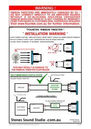
5. Application Circuit<br />
6. Applicable optical fiber with fiber optic connectors<br />
TOCP172−□□B<br />
7. Precautions during use<br />
(1) Maximum rating<br />
The maximum ratings are the limit values which must not be exceeded when using the device. Any<br />
one of the rating must not be exceeded. If The maximum rating is exceeded, the characteristics may<br />
not be recovered. In some extreme cases, the device may be permanently damage.<br />
(2) Life of light emitters<br />
When the optical module is used for over a long period, degeneration of characteristics is mostly due<br />
to lowering of the fiber output power (Pf). This is caused by the degradation of the optical output of<br />
the LED’s used as the light source. The cause of degradation of the optical output of the LED’ may be<br />
defects in wafer crystallization or mold resin stress. The detailed causes are, however, not clear.<br />
The life of light emitters is greatly influenced by operating conditions and usage environment as well<br />
as the life characteristics unique to the device. Thus, when selecting a light emitter and setting the<br />
operating conditions, Toshiba recommends that you check the life characteristics.<br />
Depending on the environment conditions, Toshiba recommends maintenance such as regular checks<br />
on the amount of optical output.<br />
(3) Soldering<br />
Optical modules use semiconductor devices internally. However, in principle, optical modules are<br />
optical components. At soldering, take care that flux dose not contact the emitting surface or detecting<br />
surface. Also take care at flux removal after soldering.<br />
Some optical modules come with protective cap. The protective cap is used to avoid malfunction when<br />
the optical module is not in use. Not that it is not dust or waterproof.<br />
As mentioned before, optical modules are optical component. Thus, in principle, soldering where there<br />
may be flux residue or flux removal after soldering is not recommended. Toshiba recommends that<br />
soldering be performed without the optical module mounted on the board. Then, after the board is<br />
cleaned, solder the optical module manually. Do not perform any further cleaning.<br />
If the optical module cannot be soldered manually, use non−halogen (chlorine−free) flux and make<br />
sure, without cleaning, there is no residue such as chlorine. This is one of the ways to eliminate the<br />
effects of flux.<br />
(4) Vibration and shock<br />
This module is resin−molded construction with wire fixed by resin. This structure is relatively sound<br />
against vibration or shock, In actual equipment, there are some cases where vibration, shock, and<br />
stress is applied to soldered parts or connected parts, resultingin line cut. Attention must be paid to<br />
the design of the mechanism for applications which are subject to large amounts of vibration.<br />
(5) Fixing fiber optical transceiving module<br />
Solder the fixed pin (pins 5 and 6) of fiber optic transmitting module <strong>TOTX173</strong> to the printed circuit<br />
board to fix the module to the board.<br />
3<br />
2001-08-10
<strong>TOTX173</strong><br />
(6) Solvent<br />
When using solvent for flux removal, do not use a high acid or high alkali solvent. Be careful not to<br />
pour solvent in the optical connector ports. If solvent is inadvertently poured there, clean with cotton<br />
tips.<br />
(7) Protective cap<br />
When the fiber optic transmitting module <strong>TOTX173</strong> is not in use, use the protective cap.<br />
(8) Supply Voltage<br />
Use the supply voltage within the Typ. operating condition (VCC = 5 ± 0.25 V). Make sure that supply<br />
voltage does not exceed the maximum rating value of 7 V, even instantaneously.<br />
(9) Input voltage<br />
If a voltage exceeding the maximum rating value (VCC + 0.5V) is applied to the transmitter input, the<br />
internal IC may degrade causing some damage. If excessive voltage due to surges may be added to the<br />
input, insert a protective circuit.<br />
(10) Soldering condition<br />
Solder at 260°C or less within ten seconds.<br />
(11) Precaution on waste<br />
When discarding devices and packing materials, follow procedures stipulated by local regulations in<br />
order to protect the environment against contamination.<br />
Compound semiconductors such as GaAs are used as LED materials for this module. When discarding<br />
waste or at final processing, attention must be paid to workers and the environment.<br />
(12) Precaution on use<br />
Toshiba is continually working to improve the quality and the reliability of its products. Nevertheless,<br />
semiconductor devices in general can malfunction or fail due to their inherent electrical sensitivity<br />
and vulnerability to physical stress. It is the responsibility of the buyer, when utilizing Toshiba<br />
products, to observe standards of safety, and to avoid situations in which a malfunction or failure of a<br />
Toshiba product could cause loss of human life, bodily injury or damage to property.<br />
In developing your designs, please ensure that Toshiba products are used within specified operating<br />
ranges as set forth in the most recent product specifications. Also, please keep in mind the<br />
precautions and conditions set forth in the Toshiba Semiconductor Reliability Handbook.<br />
4<br />
2001-08-10
<strong>TOTX173</strong><br />
RESTRICTIONS ON PRODUCT USE<br />
000707EAC<br />
TOSHIBA is continually working to improve the quality and reliability of its products. Nevertheless, semiconductor<br />
devices in general can malfunction or fail due to their inherent electrical sensitivity and vulnerability to physical<br />
stress. It is the responsibility of the buyer, when utilizing TOSHIBA products, to comply with the standards of<br />
safety in making a safe design for the entire system, and to avoid situations in which a malfunction or failure of<br />
such TOSHIBA products could cause loss of human life, bodily injury or damage to property.<br />
In developing your designs, please ensure that TOSHIBA products are used within specified operating ranges as<br />
set forth in the most recent TOSHIBA products specifications. Also, please keep in mind the precautions and<br />
conditions set forth in the “Handling Guide for Semiconductor Devices,” or “TOSHIBA Semiconductor Reliability<br />
Handbook” etc..<br />
The TOSHIBA products listed in this document are intended for usage in general electronics applications<br />
(computer, personal equipment, office equipment, measuring equipment, industrial robotics, domestic appliances,<br />
etc.). These TOSHIBA products are neither intended nor warranted for usage in equipment that requires<br />
extraordinarily high quality and/or reliability or a malfunction or failure of which may cause loss of human life or<br />
bodily injury (“Unintended Usage”). Unintended Usage include atomic energy control instruments, airplane or<br />
spaceship instruments, transportation instruments, traffic signal instruments, combustion control instruments,<br />
medical instruments, all types of safety devices, etc.. Unintended Usage of TOSHIBA products listed in this<br />
document shall be made at the customer’s own risk.<br />
Gallium arsenide (GaAs) is a substance used in the products described in this document. GaAs dust and fumes<br />
are toxic. Do not break, cut or pulverize the product, or use chemicals to dissolve them. When disposing of the<br />
products, follow the appropriate regulations. Do not dispose of the products with other industrial waste or with<br />
domestic garbage.<br />
The information contained herein is presented only as a guide for the applications of our products. No<br />
responsibility is assumed by TOSHIBA CORPORATION for any infringements of intellectual property or other<br />
rights of the third parties which may result from its use. No license is granted by implication or otherwise under<br />
any intellectual property or other rights of TOSHIBA CORPORATION or others.<br />
The information contained herein is subject to change without notice.<br />
5<br />
2001-08-10