Plasmalab®80Plus Plasmalab®800Plus - Avaco
Plasmalab®80Plus Plasmalab®800Plus - Avaco
Plasmalab®80Plus Plasmalab®800Plus - Avaco

You also want an ePaper? Increase the reach of your titles
YUMPU automatically turns print PDFs into web optimized ePapers that Google loves.
Worldwide Service and Support<br />
■ Plasma Etch & Deposition<br />
■ Atomic Layer Deposition<br />
■ Ion Beam Etch & Deposition<br />
■ Nanoscale Growth System<br />
■ HVPE Tools & Substrates<br />
Oxford Instruments<br />
Plasma Technology<br />
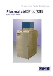
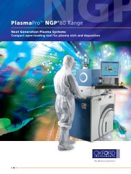
Plasmalab ® 80Plus<br />
Plasmalab ® 800Plus<br />
Compact open-loading process solutions for plasma etch and deposition<br />
Oxford Instruments is committed to supporting our customers’<br />
success. We recognise that this requires world class products<br />
complemented by world class support. Our global service force<br />
is backed by regional offices, offering rapid support wherever<br />
you are in the world.<br />
We can provide:<br />
■ Tailored service agreements to meet your needs<br />
■ Comprehensive range of structured training courses<br />
■ Immediate access to genuine spare parts and accessories<br />
■ System upgrades and refurbishments<br />
plasma@oxinst.com<br />
UK<br />
North End, Yatton,<br />
Bristol, BS49 4AP<br />
Tel: +44 (0)1934 837000<br />
Fax: +44 (0)1934 837001<br />
Email: plasma@oxinst.com<br />
Germany<br />
Wiesbaden<br />
Tel: +49 (0)6122 937 161<br />
Fax: +49 (0)6122 937 175<br />
Japan<br />
Tokyo<br />
Tel: +81 3 5245 3261<br />
Fax: +81 3 5245 4466<br />
PR China<br />
Beijing<br />
Tel: +86 10 6518 8160/1/2<br />
Fax: +86 10 6518 8155<br />
Shanghai<br />
Tel: +86 21 6360 8530<br />
Fax: +86 21 6360 8535<br />
click onto www.oxford-instruments.com for more information<br />
Oxford Instruments, at Yatton, UK, operates Quality Management Systems approved to the requirements of BS EN ISO 9001. This publication is the copyright<br />
of Oxford Instruments Plasma Technology Limited and provides outline information only which (unless agreed by the company in writing) may not be used,<br />
applied or reproduced for any purpose or form part of any order or contract or be regarded as a representation relating to the products or services concerned.<br />
Oxford Instruments’ policy is one of continued improvement. The company reserves the right to alter, without notice, the specification, design or conditions of<br />
supply of any product or service. Oxford Instruments acknowledges all trade marks and registrations.<br />
© Oxford Instruments Plasma Technology Ltd, 2009. All rights reserved.<br />
Plasmalab is a registered trademark of Oxford Instruments Plasma Technology Ltd.<br />
Ref: OIPT/80/2009/01<br />
Singapore<br />
Tel: +65 6337 6848<br />
Fax: +65 6337 6286<br />
USA<br />
Concord, MA<br />
TOLLFREE +1 800 447 4717<br />
Fax: +1 978 369 8287<br />
www.oxford-instruments.com<br />
As part of<br />
Oxford Instruments’<br />
environmental policy<br />
this brochure has been<br />
printed on FSC paper<br />
The Business of Science ®
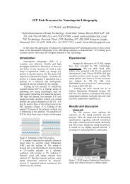
RIE of InP waveguide<br />
The Plasmalab80Plus and Plasmalab800Plus offer<br />
versatile plasma etch and deposition solutions with<br />
convenient open loading in a compact, small-footprint<br />
system, making them easy to site and easy to use,<br />
with no compromise on process quality.<br />
Deep Si feature etch by<br />
ICP-RIE cryo process<br />
Sub µm Si mesa etch<br />
Sub-µm Nb metal RIE (PR<br />
mask still in place)<br />
7 µm polyimide feature RIE<br />
RIE of In P with Si0 2 mask<br />
Failure analysis - fast metal<br />
layer exposure in the<br />
PlasmalabµEtchICP<br />
Plasmalab80Plus<br />
The Plasmalab80Plus is ideally suited to R&D or small-scale<br />
production, with 240 mm diameter table allowing 200 mm (8”)<br />
wafer or 9 x 50 mm (2”) batch capacity.<br />
The open-load design allows fast wafer loading and unloading,<br />
ideal for research, prototyping and low-volume production.<br />
Plasmalab800Plus<br />
The Plasmalab800Plus with 380 mm or 460 mm diameter table<br />
offers full 300 mm (12”) or large batch 48 x 50mm (2”) capacity,<br />
enabling full production solutions in a small cleanroom footprint.<br />
Wide range of applications<br />
Applications include:<br />
■<br />
■<br />
■<br />
■<br />
■<br />
■<br />
■<br />
SiO2, SiNx and quartz etch<br />
Metal etch<br />
Polyimide etch<br />
High quality PECVD of silicon nitride and silicon dioxide for<br />
photonics, dielectric layers, passivation and many other<br />
applications<br />
Hard mask deposition and etch for high brightness LED<br />
production<br />
Failure analysis dry etch de-processing using the speciallyconfigured<br />
PlasmalabµEtch tools, with RIE, dual-mode<br />
RIE/PE and ICP processes ranging from packaged chip and<br />
die etch through to full 300 mm wafer etch<br />
III-V etch processes (with optional glovebox to enhance<br />
safety of toxic gas use)<br />
Plasmalab80Plus<br />
RIE Tool<br />
RIE<br />
Reactive<br />
Inductively Coupled<br />
ICP<br />
Plasmalab80Plus<br />
ICP Etch Tool<br />
Ion Etching<br />
ETCHING<br />
Plasmalab80Plus<br />
Plasmalab800Plus<br />
Multiple process<br />
solutions<br />
Plasma<br />
Plasma<br />
Dual-Mode Etching<br />
D EPO SITIO N<br />
etch RIE/PE<br />
PECVD<br />
Plasma Enhanced Chemical Vapour Deposition<br />
Plasmalab800Plus<br />
PECVD Tool<br />
Plasmalab800Plus<br />
Dual-Mode PE/RIE Tool<br />
Plasma Etch & Deposition Atomic Layer Deposition Ion Beam Etch & Deposition Nanoscale Growth Systems HVPE
System benefits<br />
Substrate temperature control<br />
■<br />
■<br />
■<br />
Substrate temperature control is provided by<br />
a range of fluid-cooled and/or electricallyheated<br />
electrodes, with a temperature<br />
range up to 400 °C and excellent electrode<br />
temperature control and stability<br />
On the Plasmalab80Plus, options are<br />
available for helium-assisted substrate<br />
backside cooling, for optimum temperature<br />
control during processes<br />
Cooling on the Plasmalab80Plus can be<br />
further extended down to -150 °C with the<br />
cryogenic electrode option, enabling Si<br />
cryo-etch processes<br />
PECVD stress control<br />
■<br />
■<br />
Etch end-point detection<br />
Excellent etch control and rate<br />
determination can be provided by<br />
optional end-point detection, integrated<br />
with the PC2000 TM process tool software.<br />
Laser end-point detection using interferometry to measure<br />
etch depth in transparent materials on reflective surfaces (for<br />
example, oxides on Si), or reflectometry for non-transparent<br />
materials (such as metals) to determine layer boundaries<br />
Optical emission spectrometry (OES) for large sample or batch<br />
process end-pointing by detecting changes in etch by-products<br />
or depletion of reactive gas<br />
species, and for chamber<br />
clean end-pointing<br />
■<br />
Stress control in PECVD is provided by<br />
selectable or mixed high/low frequency plasma<br />
power, enabling deposited films to be tuned<br />
for tensile, compressive or low stress<br />
Flexible gas line options<br />
■<br />
■<br />
4-, 8- or 12-line gas pod options<br />
enable maximum process flexibility,<br />
with easy upgrade from 4 to 8 or 8<br />
to 12 gas lines<br />
The gas pod may be sited remotely in<br />
a service area, and is vented and<br />
ready for ducting into an extraction<br />
system for full safety compliance<br />
Plasma Etch & Deposition Atomic Layer Deposition Ion Beam Etch & Deposition Nanoscale Growth Systems HVPE
Optimised plasma sources<br />
The electrostatic shield design in the<br />
Plasmalab80Plus ICP configuration avoids<br />
energetic ion bombardment and capacitive<br />
coupling, providing low substrate damage,<br />
with long life for the ICP tube and reduced<br />
maintenance.<br />
Optimised showerhead design delivers high<br />
performance PECVD processes with excellent<br />
deposition uniformity.<br />
Easy open access<br />
■<br />
Clear access to the lower electrode and smooth, particlefree<br />
chamber opening operation is provided by the reliable<br />
pneumatic hoist mechanism<br />
High performance processes<br />
■<br />
■<br />
■<br />
Enhanced process uniformity and rates are guaranteed by<br />
using a high-conductance radial (axially symmetric)<br />
pumping configuration<br />
Optimised plasma conditions are enabled by three levels<br />
of control of matching capacitor values:<br />
- easy, automatic plasma generation using full automatic<br />
matching network<br />
- faster switch-over between widely differing processes<br />
using the range of preset capacitor values<br />
- process fine-tuning and diagnostics through the use of<br />
recipe-settable capacitor values in the PC2000 TM software<br />
The addition of datalogging of the capacitor values<br />
offers traceability and history of chamber and process<br />
conditions.<br />
A close-coupled turbo pump provides high pumping<br />
speed and excellent base pressure<br />
Easy maintenance<br />
■<br />
Easy access to main components for maintenance<br />
through removable panels on each side<br />
Range of electrode sizes and wafer capacity<br />
Plasmalab80Plus<br />
Plasmalab800Plus<br />
Wafer stage 240 mm 380 mm 460 mm<br />
(lower electrode) sizes<br />
Wafer loading capacity*<br />
50 mm/2” 9 30 > 40<br />
75 mm/3” 4 13 21<br />
100 mm/4” 2 8 12<br />
150 mm/6” 1 3 5<br />
200 mm/8” 1 1 2<br />
300 mm/12” - 1 1<br />
* maximum, actual loading is process-dependent<br />
Multiple process configurations<br />
Plasmalab80Plus<br />
PECVD x x<br />
RIE x x<br />
RIE/PE dual mode x x<br />
ICP<br />
x<br />
Plasmalab800Plus<br />
Cost of ownership<br />
High performance and excellent<br />
uniformity processes mean<br />
increased productivity and tool<br />
utilisation. Together with<br />
excellent reliability, these create<br />
low cost of ownership for<br />
Oxford Instruments’ process<br />
tools. Supported by Oxford<br />
Instruments’ preventative<br />
maintenance and service<br />
contract packages, the ultimate<br />
in system uptime can be assured.<br />
Process tool software<br />
Oxford Instruments’ PC2000 TM<br />
software is clear, easy to use,<br />
quick to learn and configured<br />
exactly for the customer’s<br />
system. Its visual interface<br />
controls and monitors the<br />
process tool, and offers the<br />
ability to control a tool cluster<br />
from a single interface and PC.<br />
Process ‘recipes’ are written,<br />
stored and recalled through<br />
the same software, building<br />
into a process library. In<br />
cassette-to-cassette and cluster<br />
systems, the users can associate<br />
individual recipes with each<br />
wafer to be processed, and run<br />
a complete set of process steps,<br />
loops and repeats. Passwordcontrolled<br />
user login allows<br />
different levels of user access<br />
and tasks, from ‘one-button’<br />
run operation to full system<br />
functions. Continuous process<br />
data logging ensures<br />
traceability of each wafer and<br />
process GEM/SECS compatible.<br />
Plasma Etch & Deposition Atomic Layer Deposition Ion Beam Etch & Deposition Nanoscale Growth Systems HVPE