PIC12F629/675 EEPROM Memory Programming Specification
PIC12F629/675 EEPROM Memory Programming Specification
PIC12F629/675 EEPROM Memory Programming Specification

Create successful ePaper yourself
Turn your PDF publications into a flip-book with our unique Google optimized e-Paper software.
<strong>PIC12F629</strong>/<strong>675</strong><br />
<strong>EEPROM</strong> <strong>Memory</strong> <strong>Programming</strong> <strong>Specification</strong><br />
This document includes the<br />
programming specifications for the<br />
following devices:<br />
• <strong>PIC12F629</strong><br />
• PIC12F<strong>675</strong><br />
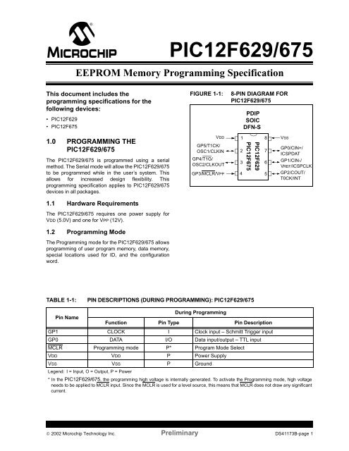
FIGURE 1-1:<br />
8-PIN DIAGRAM FOR<br />
<strong>PIC12F629</strong>/<strong>675</strong><br />
PDIP<br />
SOIC<br />
DFN-S<br />
1.0 PROGRAMMING THE<br />
<strong>PIC12F629</strong>/<strong>675</strong><br />
The <strong>PIC12F629</strong>/<strong>675</strong> is programmed using a serial<br />
method. The Serial mode will allow the <strong>PIC12F629</strong>/<strong>675</strong><br />
to be programmed while in the user’s system. This<br />
allows for increased design flexibility. This<br />
programming specification applies to <strong>PIC12F629</strong>/<strong>675</strong><br />
devices in all packages.<br />
VDD<br />
GP5/T1CK/<br />
OSC1/CLKIN<br />
GP4/T1G/<br />
OSC2/CLKOUT<br />
GP3/MCLR/VPP<br />
1 8<br />
2<br />
3<br />
PIC12F<strong>675</strong><br />
<strong>PIC12F629</strong><br />
7<br />
6<br />
4 5<br />
VSS<br />
GP0/CIN+/<br />
ICSPDAT<br />
GP1/CIN-/<br />
VREF/ICSPCLK<br />
GP2/COUT/<br />
T0CK/INT<br />
1.1 Hardware Requirements<br />
The <strong>PIC12F629</strong>/<strong>675</strong> requires one power supply for<br />
VDD (5.0V) and one for VPP (12V).<br />
1.2 <strong>Programming</strong> Mode<br />
The <strong>Programming</strong> mode for the <strong>PIC12F629</strong>/<strong>675</strong> allows<br />
programming of user program memory, data memory,<br />
special locations used for ID, and the configuration<br />
word.<br />
TABLE 1-1:<br />
PIN DESCRIPTIONS (DURING PROGRAMMING): <strong>PIC12F629</strong>/<strong>675</strong><br />
During <strong>Programming</strong><br />
Pin Name<br />
Function Pin Type Pin Description<br />
GP1 CLOCK I Clock input – Schmitt Trigger input<br />
GP0 DATA I/O Data input/output – TTL input<br />
MCLR <strong>Programming</strong> mode P* Program Mode Select<br />
VDD VDD P Power Supply<br />
VSS VSS P Ground<br />
Legend: I = Input, O = Output, P = Power<br />
* In the <strong>PIC12F629</strong>/<strong>675</strong>, the programming high voltage is internally generated. To activate the <strong>Programming</strong> mode, high voltage<br />
needs to be applied to MCLR input. Since the MCLR is used for a level source, this means that MCLR does not draw any significant<br />
current.<br />
© 2002 Microchip Technology Inc. Preliminary DS41173B-page 1
<strong>PIC12F629</strong>/<strong>675</strong><br />
2.0 PROGRAM MODE ENTRY<br />
2.1 User Program <strong>Memory</strong> Map<br />
The user memory space extends from 0x0000 to<br />
0x1FFF. In <strong>Programming</strong> mode, the program memory<br />
space extends from 0x0000 to 0x3FFF, with the first<br />
half (0x0000-0x1FFF) being user program memory and<br />
the second half (0x2000-0x3FFF) being configuration<br />
memory. The PC will increment from 0x0000 to 0x1FFF<br />
and wrap to 0x000, 0x2000 to 0x3FFF and wrap<br />
around to 0x2000 (not to 0x0000). Once in configuration<br />
memory, the highest bit of the PC stays a ‘1’, thus<br />
always pointing to the configuration memory. The only<br />
way to point to user program memory is to RESET the<br />
part and re-enter Program/Verify mode as described in<br />
Section 2.3.<br />
In the configuration memory space, 0x2000-0x200F<br />
are physically implemented. However, only locations<br />
0x2000 through 0x2003, and 0x2007 are available.<br />
Other locations are reserved.<br />
2.2 ID Locations<br />
A user may store identification information (ID) in four<br />
ID locations. The ID locations are mapped in [0x2000 :<br />
0x2003]. It is recommended that the user use only the<br />
seven Least Significant bits of each ID location. Locations<br />
read out normally, even after code protection. The<br />
ID locations read out in an unscrambled fashion after<br />
code protection is enabled. It is recommended that ID<br />
location is written as “xx xxxx xbbb bbbb” where<br />
‘bbb bbbb’ is ID information.<br />
The 14 bits may be programmed, but only the LSb’s are<br />
displayed by MPLAB ® IDE. xxxx’s are “don’t care” bits<br />
as they won’t be read by MPLAB IDE.<br />
FIGURE 2-1:<br />
PROGRAM MEMORY MAPPING<br />
1 KW<br />
03FF<br />
OSCCAL<br />
03FE<br />
03FF<br />
Implemented<br />
Implemented<br />
400<br />
Not Implemented<br />
2000<br />
2001<br />
ID Location<br />
ID Location<br />
1FFF<br />
2000<br />
2008<br />
Implemented<br />
2002<br />
ID Location<br />
2003<br />
ID Location<br />
2004<br />
Reserved<br />
Not Implemented<br />
2005<br />
Reserved<br />
2006<br />
Reserved<br />
2007<br />
Configuration Word<br />
3FFF<br />
DS41173B-page 2 Preliminary © 2002 Microchip Technology Inc.
<strong>PIC12F629</strong>/<strong>675</strong><br />
2.3 Program/Verify Mode<br />
The Program/Verify mode is entered by holding pins<br />
CLOCK and DATA low while raising MCLR pin from VIL<br />
to VIHH (high voltage). Apply VDD and data. Once in this<br />
mode, the user program memory, data memory and the<br />
configuration memory can be accessed and programmed<br />
in serial fashion. CLOCK is Schmitt Trigger<br />
and DATA is TTL input in this mode. GP4 is tristate,<br />
regardless of fuse setting.<br />
The sequence that enters the device into the <strong>Programming</strong>/Verify<br />
mode places all other logic into the RESET<br />
state (the MCLR pin was initially at VIL). This means<br />
that all I/O are in the RESET state (hi-impedance<br />
inputs).<br />
FIGURE 2-2:<br />
VPP<br />
VDD<br />
DATA<br />
CLOCK<br />
ENTERING HIGH VOLTAGE<br />
PROGRAM/VERIFY MODE<br />
Tppdp<br />
Thld0<br />
SDATA = Input<br />
The normal sequence for programming is to use the<br />
LOAD DATA command to set a value to be written at<br />
the selected address. Issue the BEGIN<br />
PROGRAMING command followed by READ DATA<br />
command to verify and then increment the address.<br />
A device RESET will clear the PC and set the address<br />
to ‘0’. The INCREMENT ADDRESS command will<br />
increment the PC. The LOAD CONFIGURATION<br />
command will set the PC to 0x2000. The available<br />
commands are shown in Table 2-1.<br />
2.3.1 SERIAL PROGRAM/VERIFY<br />
OPERATION<br />
The CLOCK pin is used as a clock input pin, and the<br />
DATA pin is used for entering command bits and data<br />
input/output during serial operation. To input a command,<br />
the clock pin (CLOCK) is cycled six times. Each<br />
command bit is latched on the falling edge of the clock<br />
with the Least Significant bit (LSb) of the command<br />
being input first. The data on pin DATA is required to<br />
have a minimum setup and hold time (see AC/DC<br />
specifications), with respect to the falling edge of the<br />
clock. Commands that have data associated with them<br />
(read and load) are specified to have a minimum delay<br />
of 1 µs between the command and the data. After this<br />
delay, the clock pin is cycled 16 times with the first cycle<br />
being a START bit and the last cycle being a STOP bit.<br />
Data is also input and output LSb first.<br />
Therefore, during a read operation the LSb will be<br />
transmitted onto pin DATA on the rising edge of the<br />
second cycle, and during a load operation the LSb will<br />
be latched on the falling edge of the second cycle. A<br />
minimum 1 µs delay is also specified between<br />
consecutive commands.<br />
All commands are transmitted LSb first. Data words<br />
are also transmitted LSb first. The data is transmitted<br />
on the rising edge and latched on the falling edge of<br />
the clock. To allow for decoding of commands and<br />
reversal of data pin configuration, a time separation of<br />
at least 1 µs is required between a command and a<br />
data word (or another command).<br />
TABLE 2-1: COMMAND MAPPING FOR <strong>PIC12F629</strong>/<strong>675</strong><br />
Command Mapping (MSb … LSb) Data<br />
LOAD CONFIGURATION X X 0 0 0 0 0, data (14), 0<br />
LOAD DATA FOR PROGRAM MEMORY X X 0 0 1 0 0, data (14), 0<br />
LOAD DATA FOR DATA MEMORY X X 0 0 1 1 0, data (8), zero (6), 0<br />
READ DATA FROM PROGRAM MEMORY X X 0 1 0 0 0, data (14), 0<br />
READ DATA FROM DATA MEMORY X X 0 1 0 1 0, data (8), zero (6), 0<br />
INCREMENT ADDRESS X X 0 1 1 0<br />
BEGIN PROGRAMMING 0 0 1 0 0 0<br />
BULK ERASE PROGRAM MEMORY X X 1 0 0 1<br />
BULK ERASE DATA MEMORY X X 1 0 1 1<br />
© 2002 Microchip Technology Inc. Preliminary DS41173B-page 3
<strong>PIC12F629</strong>/<strong>675</strong><br />
2.3.1.1 LOAD CONFIGURATION<br />
After receiving this command, the program counter<br />
(PC) will be set to 0x2000. Then, by applying 16 cycles<br />
to the clock pin, the chip will load 14 bits in a “data<br />
word,” as described above, which will be programmed<br />
into the configuration memory. A description of the<br />
memory mapping schemes of the program memory for<br />
normal operation and Configuration mode operation is<br />
shown in Figure 2-1. After the configuration memory is<br />
entered, the only way to get back to the user program<br />
memory is to exit the Program/Verify mode by taking<br />
MCLR low (VIL).<br />
FIGURE 2-3:<br />
LOAD CONFIGURATION COMMAND<br />
GP1<br />
CLOCK<br />
1 2 3 4 5 6<br />
Tdly2<br />
1 2 3 4 5 15 16<br />
GP0<br />
DATA<br />
0 00 0 0 X X<br />
Tdly1<br />
strt_bit<br />
LSb<br />
Tset1<br />
Thld1<br />
MSb<br />
stp_bit<br />
2.3.1.2 LOAD DATA FOR PROGRAM<br />
MEMORY<br />
After receiving this command, the chip will load in a<br />
14-bit “data word” when 16 cycles are applied, as<br />
described previously. A timing diagram for the LOAD<br />
DATA command is shown in Figure 2-4.<br />
FIGURE 2-4:<br />
LOAD DATA FOR PROGRAM MEMORY COMMAND<br />
GP1<br />
CLOCK<br />
1 2 3 4 5 6<br />
Tdly2<br />
1 2 3 4 5 15 16<br />
GP0<br />
DATA<br />
0 1 0 0 X X<br />
Tset1<br />
Tdly1<br />
Thld1<br />
strt_bit<br />
LSb<br />
Tset1<br />
Thld1<br />
MSb<br />
stp_bit<br />
DS41173B-page 4 Preliminary © 2002 Microchip Technology Inc.
<strong>PIC12F629</strong>/<strong>675</strong><br />
2.3.1.3 LOAD DATA FOR DATA MEMORY<br />
After receiving this command, the chip will load in a<br />
14-bit “data word” when 16 cycles are applied.<br />
However, the data memory is only 8 bits wide and thus,<br />
only the first 8 bits of data after the START bit will be<br />
programmed into the data memory. It is still necessary<br />
to cycle the clock the full 16 cycles in order to allow the<br />
internal circuitry to reset properly. The data memory<br />
contains 128 bytes. Only the lower 8 bits of the PC are<br />
decoded by the data memory, and therefore, if the PC<br />
is greater than 0x7F, it will wrap around and address a<br />
location within the physically implemented memory.<br />
FIGURE 2-5:<br />
LOAD DATA FOR DATA MEMORY COMMAND<br />
Tdly2<br />
GP1<br />
CLOCK<br />
GP0<br />
DATA<br />
1 2 3 4 5 6<br />
1 1 0 0 X X<br />
1 2 3 4 5 15 16<br />
Tdly3<br />
strt_bit<br />
Tdly1<br />
LSb<br />
MSb<br />
stp_bit<br />
input output input<br />
2.3.1.4 READ DATA FROM PROGRAM<br />
MEMORY<br />
After receiving this command, the chip will transmit<br />
data bits out of the program memory (user or<br />
configuration) currently accessed, starting with the<br />
second rising edge of the clock input. The DATA pin will<br />
go into Output mode on the second rising clock edge,<br />
and it will revert to Input mode (hi-impedance) after the<br />
16th rising edge.<br />
If the program memory is code protected (CP = 0), the<br />
data is read as zeros.<br />
FIGURE 2-6:<br />
READ DATA FROM PROGRAM MEMORY COMMAND<br />
Tdly2<br />
GP1<br />
CLOCK<br />
GP0<br />
DATA<br />
1 2 3 4 5 6<br />
1 0 0 1 0 X X<br />
Tset1<br />
1 2 3 4 5 15 16<br />
Tdly3<br />
strt_bit<br />
Tdly1<br />
LSb<br />
MSb<br />
stp_bit<br />
Thld1<br />
input output input<br />
© 2002 Microchip Technology Inc. Preliminary DS41173B-page 5
<strong>PIC12F629</strong>/<strong>675</strong><br />
2.3.1.5 READ DATA FROM DATA<br />
MEMORY<br />
After receiving this command, the chip will transmit<br />
data bits out of the data memory starting with the<br />
second rising edge of the clock input. The DATA pin will<br />
go into Output mode on the second rising edge, and it<br />
will revert to Input mode (hi-impedance) after the 16th<br />
rising edge. As previously stated, the data memory is 8<br />
bits wide, and therefore, only the first 8 bits that are<br />
output are actual data. If the data memory is code<br />
protected, the data is read as all zeros. A timing<br />
diagram of this command is shown in Figure 2-7.<br />
FIGURE 2-7:<br />
READ DATA FROM DATA MEMORY COMMAND<br />
Tdly2<br />
GP1<br />
CLOCK<br />
GP0<br />
DATA<br />
1 2 3 4 5 6<br />
1 0 1 0 X X<br />
Tset1<br />
1 2 3 4 5 15 16<br />
Tdly3<br />
strt_bit<br />
Tdly1<br />
LSb<br />
MSb<br />
stp_bit<br />
Thld1<br />
input output input<br />
2.3.1.6 INCREMENT ADDRESS<br />
The PC is incremented when this command is<br />
received. A timing diagram of this command is shown<br />
in Figure 2-8.<br />
It is not possible to decrement the address counter. To<br />
reset this counter, the user should exit and re-enter<br />
<strong>Programming</strong> mode.<br />
FIGURE 2-8:<br />
INCREMENT ADDRESS COMMAND (PROGRAM/VERIFY)<br />
Tdly2<br />
Next Command<br />
1 2 3 4 5 6<br />
1 2<br />
GP1<br />
CLOCK<br />
GP0<br />
DATA<br />
0 1 1 0 X X<br />
Tset1<br />
Tdly1<br />
X 0<br />
Thld1<br />
DS41173B-page 6 Preliminary © 2002 Microchip Technology Inc.
<strong>PIC12F629</strong>/<strong>675</strong><br />
2.3.1.7 BEGIN PROGRAMMING<br />
A load command must be given before every<br />
BEGIN PROGRAMMING command. <strong>Programming</strong><br />
of the appropriate memory (user program memory or<br />
data memory) will begin after this command is received<br />
and decoded. An internal timing mechanism executes<br />
a write. The user must allow for program cycle time for<br />
programming to complete. No END PROGRAMMING<br />
command is required.<br />
When programming data memory, the byte being<br />
addressed is erased before being programmed.<br />
FIGURE 2-9:<br />
BEGIN PROGRAMMING COMMAND (PROGRAM/VERIFY)<br />
GP1<br />
CLOCK<br />
Tprog<br />
Next Command<br />
1 2 3 4 5 6 1 2<br />
GP0<br />
DATA<br />
0 0 0 1 0 0<br />
Tset1<br />
Tdly1<br />
X 0<br />
Thld1<br />
Program/Verify Test Mode<br />
© 2002 Microchip Technology Inc. Preliminary DS41173B-page 7
<strong>PIC12F629</strong>/<strong>675</strong><br />
2.3.1.8 BULK ERASE PROGRAM<br />
MEMORY<br />
After this command is performed and calibration bits<br />
are erased, the entire program memory is erased. If<br />
data is code protected, data memory will also be<br />
erased.<br />
Note:<br />
The OSCCAL word and BG bits must be<br />
read prior to erasing the device and<br />
restored during the programming<br />
operation. OSCCAL is at location 0x3FF<br />
and the BG bits are bits 12 and 13 of the<br />
configuration word (0x2007).<br />
To perform a bulk erase of the program memory, the<br />
following sequence must be performed.<br />
1. Read OSCCAL 0x3FF.<br />
2. Read configuration word.<br />
3. Do a BULK ERASE PROGRAM MEMORY<br />
command.<br />
4. Wait Tera to complete bulk erase.<br />
If the address is pointing to the ID/configuration<br />
program memory (0x2000 - 0x200F), then both the<br />
user memory and the ID locations will be erased.<br />
FIGURE 2-10:<br />
BULK ERASE PROGRAM MEMORY COMMAND<br />
GP1<br />
CLOCK<br />
Tera<br />
Next Command<br />
1 2 3 4 5 6 1 2<br />
GP0<br />
DATA<br />
Tset1<br />
1 0 0 1 X X<br />
Tset1<br />
Tdly1<br />
X 0<br />
Thld1<br />
Thld1<br />
Program/Verify Test Mode<br />
DS41173B-page 8 Preliminary © 2002 Microchip Technology Inc.
<strong>PIC12F629</strong>/<strong>675</strong><br />
2.3.1.9 BULK ERASE DATA MEMORY<br />
To perform a bulk erase of the data memory, the<br />
following sequence must be performed.<br />
1. Do a BULK ERASE DATA MEMORY<br />
command.<br />
2. Wait Tera to complete bulk erase.<br />
Data memory won’t erase if code protected (CPD = 0).<br />
Note:<br />
All BULK ERASE operations must take<br />
place at 4.5V to 5.5V VDD range for<br />
<strong>PIC12F629</strong>/<strong>675</strong> devices and 2.0V to 5.5V<br />
VDD for <strong>PIC12F629</strong>/<strong>675</strong>-ICD devices.<br />
FIGURE 2-11:<br />
BULK ERASE DATA MEMORY COMMAND<br />
GP1<br />
CLOCK<br />
Tera<br />
Next Command<br />
1 2 3 4 5 6 1 2<br />
GP0<br />
DATA<br />
1 1 0 1 X X<br />
Tset1<br />
Tdly1<br />
X 0<br />
Thld1<br />
Program/Verify Test Mode<br />
© 2002 Microchip Technology Inc. Preliminary DS41173B-page 9
<strong>PIC12F629</strong>/<strong>675</strong><br />
FIGURE 2-12:<br />
PROGRAM FLOW CHART - <strong>PIC12F629</strong>/<strong>675</strong> PROGRAM MEMORY<br />
Start<br />
Read and Save<br />
OSCCAL value<br />
Read and Save<br />
Bandgap Cal.<br />
Value<br />
Bulk Erase<br />
Device<br />
Program Cycle<br />
PROGRAM CYCLE<br />
LOAD DATA<br />
for<br />
Program <strong>Memory</strong><br />
READ DATA<br />
from<br />
Program <strong>Memory</strong><br />
BEGIN<br />
PROGRAMMING<br />
Command<br />
Data Correct<br />
No<br />
Report<br />
<strong>Programming</strong><br />
Failure<br />
Wait Tprog<br />
Yes<br />
INCREMENT<br />
ADDRESS<br />
Command<br />
No<br />
All Locations<br />
Done<br />
Program<br />
OSCCAL<br />
Program Data<br />
<strong>Memory</strong><br />
(if required)<br />
Verify all<br />
Locations<br />
Data Correct<br />
Yes<br />
Program<br />
Bandgap Cal.<br />
and Config bits<br />
No<br />
Report Verify<br />
Error<br />
Done<br />
DS41173B-page 10 Preliminary © 2002 Microchip Technology Inc.
<strong>PIC12F629</strong>/<strong>675</strong><br />
FIGURE 2-13:<br />
PROGRAM FLOW CHART - <strong>PIC12F629</strong>/<strong>675</strong> CONFIGURATION MEMORY<br />
Start<br />
Load<br />
Configuration<br />
Data<br />
Program Cycle<br />
READ DATA<br />
Command<br />
Data Correct<br />
No<br />
Report<br />
<strong>Programming</strong><br />
Failure<br />
Yes<br />
INCREMENT<br />
ADDRESS<br />
Command<br />
No<br />
Address =<br />
0x2004<br />
Yes<br />
INCREMENT<br />
ADDRESS<br />
Command<br />
INCREMENT<br />
ADDRESS<br />
Command<br />
INCREMENT<br />
ADDRESS<br />
Command<br />
Set Bits 12 and<br />
13 to Saved<br />
Bandgap Bits<br />
Program<br />
Cycle<br />
(config. word)<br />
READ DATA<br />
Command<br />
Data Correct<br />
Yes<br />
Done<br />
No<br />
Report<br />
<strong>Programming</strong><br />
Failure<br />
© 2002 Microchip Technology Inc. Preliminary DS41173B-page 11
<strong>PIC12F629</strong>/<strong>675</strong><br />
FIGURE 2-14:<br />
PROGRAM FLOW CHART - <strong>PIC12F629</strong>/<strong>675</strong> DATA MEMORY<br />
Start<br />
PROGRAM CYCLE<br />
Program Cycle<br />
LOAD DATA<br />
for<br />
Data <strong>Memory</strong><br />
READ DATA<br />
from<br />
Data <strong>Memory</strong><br />
BEGIN<br />
PROGRAMMING<br />
Command<br />
Data Correct<br />
No<br />
Report<br />
<strong>Programming</strong><br />
Failure<br />
Wait Tprog<br />
Yes<br />
INCREMENT<br />
ADDRESS<br />
Command<br />
No<br />
All Locations<br />
Done<br />
Yes<br />
Done<br />
DS41173B-page 12 Preliminary © 2002 Microchip Technology Inc.
<strong>PIC12F629</strong>/<strong>675</strong><br />
FIGURE 2-15:<br />
PROGRAM FLOW CHART - ERASE FLASH DEVICE<br />
Start<br />
Read and Save<br />
OSCCAL Value<br />
Read and Save<br />
Band Gap Cal<br />
Value<br />
Bulk Erase Device<br />
Program<br />
OSCCAL<br />
Program<br />
Band Gap Cal<br />
Bits<br />
Done<br />
© 2002 Microchip Technology Inc. Preliminary DS41173B-page 13
<strong>PIC12F629</strong>/<strong>675</strong><br />
3.0 CONFIGURATION WORD<br />
The <strong>PIC12F629</strong>/<strong>675</strong> has several configuration bits.<br />
These bits can be programmed (reads ‘0’), or left<br />
unchanged (reads ‘1’), to select various device<br />
configurations.<br />
REGISTER 3-1:<br />
CONFIGURATION WORD FOR <strong>PIC12F629</strong>/<strong>675</strong> DEVICE<br />
R/P-1 R/P-1 U-0 U-0 U-0 R/P-1 R/P-1 R/P-1 R/P-1 R/P-1 R/P-1 R/P-1 R/P-1 R/P-1<br />
BG1 BG0 — — — CPD CP BODEN MCLRE PWRTE WDTE FOSC2 F0SC1 F0SC0<br />
bit 13 bit 0<br />
bit 13-12 BG: Bandgap Calibration bits (2)<br />
00 = Lowest Bandgap voltage<br />
...<br />
11 = Highest Bandgap voltage<br />
bit 11-9: Unimplemented: Read as ‘0’<br />
bit 8:<br />
bit 7:<br />
CPD: Code Protection Data<br />
1 = Data memory is not protected<br />
0 = Data memory is external read protected<br />
CP: Code Protection<br />
1 = Program memory is not code protected<br />
0 = Program memory is code protected<br />
bit 6: BODEN: Brown-out Detect Reset Enable bit (1)<br />
1 = BOD Reset enabled<br />
0 = BOD Reset disabled<br />
bit 5:<br />
MCLRE: MCLR Pin Function Select<br />
1 = MCLR pin is MCLR function<br />
0 = MCLR pin is alternate function, MCLR function is internally disabled.<br />
bit 4: PWRTE: Power-up Timer Enable bit (1)<br />
1 = PWRT disabled<br />
0 = PWRT enabled<br />
bit 3:<br />
bit 2-0:<br />
WDTE: Watchdog Timer Enable bit<br />
1 = WDT enabled<br />
0 = WDT disabled<br />
FOSC: Oscillator Selection bits<br />
000 = LP oscillator: Low power crystal on GP5/T1CKI/OSC1/CLKIN and GP4/T1G/OSC2/CLKOUT<br />
001 = XT oscillator: Crystal/resonator on GP5/T1CKI/OSC1/CLKIN and GP4/T1G/OSC2/CLKOUT<br />
010 = HS oscillator: High speed crystal/resonator on GP5/T1CKI/OSC1/CLKIN and GP4/T1G/OSC2/CLKOUT<br />
011 = EC: I/O function on GP4/T1G/OSC2/CLKOUT, CLKIN on GP5/T1CKI/OSC1/CLKIN<br />
100 = INTOSC oscillator: I/O function on GP4/T1G/OSC2/CLKOUT, I/O function on GP5/T1CKI/OSC1/CLKIN<br />
101 = INTOSC oscillator: CLKOUT function on GP4/T1G/OSC2/CLKOUT, I/O function on GP5/T1CKI/OSC1/CLKIN<br />
110 = RC oscillator: I/O function on GP4/T1G/OSC2/CLKOUT, RC on GP5/T1CKI/OSC1/CLKIN<br />
111 = RC oscillator: CLKOUT function on GP4/T1G/OSC2/CLKOUT, RC on GP5/T1CKI/OSC1/CLKIN<br />
Note1:Enabling Brown-out Detect Reset Enable does not automatically enable the Power-up Timer Enable (PWRTE).<br />
2:The Bandgap Calibration bits must be read, preserved, then replaced by the user during any bulk erase<br />
operation.<br />
Legend<br />
R = Readable bit W = Writable bit U = Unimplemented bit, read as ‘0’<br />
-n = Value at POR 1 = bit is set 0 = bit is cleared x = bit is unknown<br />
DS41173B-page 14 Preliminary © 2002 Microchip Technology Inc.
<strong>PIC12F629</strong>/<strong>675</strong><br />
3.1 Device ID Word<br />
The device ID word for the <strong>PIC12F629</strong>/<strong>675</strong> is located<br />
at 2006h.<br />
TABLE 3-1:<br />
DEVICE ID VALUES<br />
Device ID Value<br />
Device<br />
Dev<br />
Rev<br />
PIC16F629 00 1111 100 x xxxx<br />
PIC16F<strong>675</strong> 00 1111 110 x xxxx<br />
© 2002 Microchip Technology Inc. Preliminary DS41173B-page 15
<strong>PIC12F629</strong>/<strong>675</strong><br />
4.0 CODE PROTECTION<br />
For <strong>PIC12F629</strong>/<strong>675</strong> devices, once code protection is<br />
enabled, all program memory locations, except 0x3FF,<br />
read all 0’s. The ID locations and the configuration<br />
word read out in an unprotected fashion. Further programming<br />
is disabled for the entire program memory.<br />
Data memory is protected with its own code protect bit<br />
(CPD). It is possible to program the ID locations and<br />
the configuration word.<br />
4.1 Disabling Code Protection<br />
It is recommended that the following procedure be performed<br />
before any other programming is attempted. It<br />
is also possible to turn code protection off (data protect<br />
bit = 1) using this procedure. However, all data within<br />
the program memory and the data memory will be<br />
erased when this procedure is executed, and thus, the<br />
security of the data or code is not compromised.<br />
To disable code protect:<br />
a) Read and store OSCCAL and BG bits.<br />
b) Execute LOAD CONFIGURATION (000000).<br />
c) Execute BULK ERASE PROGRAM MEMORY<br />
(001001).<br />
d) Wait Tera.<br />
e) Execute BULK ERASE DATA MEMORY<br />
(001011).<br />
f) Wait Tera.<br />
g) Reset device to RESET address counter before<br />
re-programming device.<br />
h) Restore OSCCAL and BG bits.<br />
Note: To ensure system security, if CPD bit = 0,<br />
step c) will also erase data memory.<br />
4.2 Embedding Configuration Word and ID Information in the HEX File<br />
To allow portability of code, the programmer is required to read the configuration word and ID locations from the HEX<br />
file when loading the HEX file. If configuration word information was not present in the HEX file, then a simple warning<br />
message may be issued. Similarly, while saving a HEX file, configuration word and ID information must be included.<br />
An option to not include this information may be provided.<br />
Specifically for the <strong>PIC12F629</strong>/<strong>675</strong>, the <strong>EEPROM</strong> data memory should also be embedded in the HEX file (see<br />
Section 4.3.2).<br />
Microchip Technology Incorporated feels strongly that this feature is important for the benefit of the end customer.<br />
DS41173B-page 16 Preliminary © 2002 Microchip Technology Inc.
<strong>PIC12F629</strong>/<strong>675</strong><br />
4.3 Checksum Computation<br />
4.3.1 CHECKSUM<br />
Checksum is calculated by reading the contents of the<br />
<strong>PIC12F629</strong>/<strong>675</strong> memory locations and adding up the<br />
opcodes up to the maximum user addressable location,<br />
(e.g., 0x3FF for the <strong>PIC12F629</strong>/<strong>675</strong>). Any carry bits<br />
exceeding 16 bits are neglected. Finally, the configuration<br />
word (appropriately masked) is added to the<br />
checksum. Checksum computation for each member of<br />
the <strong>PIC12F629</strong>/<strong>675</strong> devices is shown in Table 4-1.<br />
The checksum is calculated by summing the following:<br />
• The contents of all program memory locations<br />
• The configuration word, appropriately masked<br />
• Masked ID locations (when applicable)<br />
The Least Significant 16 bits of this sum is the<br />
checksum.<br />
TABLE 4-1: CHECKSUM COMPUTATION<br />
Device<br />
Code<br />
Protect<br />
4.3.2 EMBEDDING DATA <strong>EEPROM</strong><br />
CONTENTS IN HEX FILE<br />
The programmer should be able to read data <strong>EEPROM</strong><br />
information from a HEX file and conversely (as an<br />
option), write data <strong>EEPROM</strong> contents to a HEX file<br />
along with program memory information and fuse<br />
information.<br />
The 128 data memory locations are logically mapped<br />
starting at address 0x2100. The format for data<br />
memory storage is one data byte per address location,<br />
LSb aligned.<br />
The following table describes how to calculate the<br />
checksum for each device. Note that the checksum calculation<br />
differs depending on the code protect setting.<br />
Since the program memory locations read out differently<br />
depending on the code protect setting, the table<br />
describes how to manipulate the actual program memory<br />
values to simulate the values that would be read<br />
from a protected device. When calculating a checksum<br />
by reading a device, the entire program memory can<br />
simply be read and summed. The configuration word<br />
and ID locations can always be read.<br />
Note:<br />
Checksum*<br />
Some older devices have an additional<br />
value added in the checksum. This is to<br />
maintain compatibility with older device<br />
programmer checksums.<br />
Blank<br />
Value<br />
0x25E6 at 0<br />
and Max<br />
Address<br />
<strong>PIC12F629</strong>/<strong>675</strong> OFF SUM[0x0000:0x3FE] + CFGW & 01FF BE00 89CE<br />
ALL CFGW & 0x01FF + SUM_ID BF7F 8B4D<br />
Legend: CFGW = Configuration Word<br />
SUM[a:b] = [Sum of locations a to b inclusive]<br />
SUM_ID = ID locations masked by 0xF then made into a 16-bit value with ID0 as the most significant nybble.<br />
For example, ID0 = 0x1, ID1 = 0x2, ID3 = 0x3, ID4 = 0x4, then SUM_ID = 0x1234<br />
*Checksum = [Sum of all the individual expressions] MODULO [0xFFFF]<br />
+ = Addition<br />
& = Bitwise AND<br />
© 2002 Microchip Technology Inc. Preliminary DS41173B-page 17
<strong>PIC12F629</strong>/<strong>675</strong><br />
5.0 PROGRAM/VERIFY MODE ELECTRICAL CHARACTERISTICS<br />
TABLE 5-1:<br />
AC/DC CHARACTERISTICS TIMING REQUIREMENTS FOR<br />
PROGRAM/VERIFY MODE<br />
Standard Operating Conditions (unless otherwise stated)<br />
Operating Temperature -40°C ≤ TA ≤ +85°C<br />
Operating Voltage 4.5V ≤ VDD ≤ 5.5V<br />
Characteristics Sym Min Typ Max Units Conditions/Comments<br />
General<br />
VDD level for word operations,<br />
program memory<br />
VDD level for word operations, data<br />
memory<br />
VDD level for bulk erase/write<br />
operations, program and data memory<br />
High voltage on MCLR for <strong>Programming</strong><br />
mode entry<br />
MCLR rise time (VSS to VHH) for<br />
<strong>Programming</strong> mode entry<br />
VDD<br />
2.0<br />
4.5<br />
5.5<br />
5.5<br />
VDD 4.5 5.5 V<br />
VDD 4.5 5.5 V<br />
VIHH VDD + 3.5 13.5 V<br />
V<br />
V<br />
Tvhhr 1.0 µs<br />
Hold time after VPP↑ Tppdp 5 µs<br />
(CLOCK, DATA) input high level VIH1 0.8 VDD V<br />
(CLOCK, DATA) input low level VIL1 0.2 VDD V<br />
CLOCK, DATA setup time before<br />
MCLR↑ (<strong>Programming</strong> mode selection Tset0 100 ns<br />
pattern setup time)<br />
CLOCK, DATA hold time after MCLR↑<br />
(<strong>Programming</strong> mode selection pattern Thld0 5 µs<br />
setup time)<br />
Serial Program/Verify<br />
Data in setup time before clock↓ Tset1 100 ns<br />
Data in hold time after clock↓ Thld1 100 ns<br />
Data input not driven to next clock<br />
input (delay required between command/data<br />
Tdly1 1.0 µs<br />
or command/command)<br />
Delay between clock↓ to clock↑ of<br />
next command or data<br />
Tdly2 1.0 µs<br />
Clock↑ to data out valid (during READ<br />
DATA)<br />
Tdly3 80 ns<br />
Erase cycle time Tera 4 8 ms<br />
<strong>Programming</strong> cycle time Tprog 4 8 ms<br />
Time delay from program to compare<br />
(HV discharge time)<br />
Tdis 0.5 µs<br />
<strong>PIC12F629</strong>/<strong>675</strong>-ICD<br />
<strong>PIC12F629</strong>/<strong>675</strong><br />
DS41173B-page 18 Preliminary © 2002 Microchip Technology Inc.
Note the following details of the code protection feature on PICmicro ® MCUs.<br />
• The PICmicro family meets the specifications contained in the Microchip Data Sheet.<br />
• Microchip believes that its family of PICmicro microcontrollers is one of the most secure products of its kind on the market today,<br />
when used in the intended manner and under normal conditions.<br />
• There are dishonest and possibly illegal methods used to breach the code protection feature. All of these methods, to our knowledge,<br />
require using the PICmicro microcontroller in a manner outside the operating specifications contained in the data sheet.<br />
The person doing so may be engaged in theft of intellectual property.<br />
• Microchip is willing to work with the customer who is concerned about the integrity of their code.<br />
• Neither Microchip nor any other semiconductor manufacturer can guarantee the security of their code. Code protection does not<br />
mean that we are guaranteeing the product as “unbreakable”.<br />
• Code protection is constantly evolving. We at Microchip are committed to continuously improving the code protection features of<br />
our product.<br />
If you have any further questions about this matter, please contact the local sales office nearest to you.<br />
Information contained in this publication regarding device<br />
applications and the like is intended through suggestion only<br />
and may be superseded by updates. It is your responsibility to<br />
ensure that your application meets with your specifications.<br />
No representation or warranty is given and no liability is<br />
assumed by Microchip Technology Incorporated with respect<br />
to the accuracy or use of such information, or infringement of<br />
patents or other intellectual property rights arising from such<br />
use or otherwise. Use of Microchip’s products as critical components<br />
in life support systems is not authorized except with<br />
express written approval by Microchip. No licenses are conveyed,<br />
implicitly or otherwise, under any intellectual property<br />
rights.<br />
Trademarks<br />
The Microchip name and logo, the Microchip logo, FilterLab,<br />
KEELOQ, microID, MPLAB, PIC, PICmicro, PICMASTER,<br />
PICSTART, PRO MATE, SEEVAL and The Embedded Control<br />
Solutions Company are registered trademarks of Microchip Technology<br />
Incorporated in the U.S.A. and other countries.<br />
dsPIC, ECONOMONITOR, FanSense, FlexROM, fuzzyLAB,<br />
In-Circuit Serial <strong>Programming</strong>, ICSP, ICEPIC, microPort,<br />
Migratable <strong>Memory</strong>, MPASM, MPLIB, MPLINK, MPSIM,<br />
MXDEV, MXLAB, PICC, PICDEM, PICDEM.net, rfPIC, Select<br />
Mode and Total Endurance are trademarks of Microchip<br />
Technology Incorporated in the U.S.A.<br />
Serialized Quick Turn <strong>Programming</strong> (SQTP) is a service mark<br />
of Microchip Technology Incorporated in the U.S.A.<br />
All other trademarks mentioned herein are property of their<br />
respective companies.<br />
© 2002, Microchip Technology Incorporated, Printed in the<br />
U.S.A., All Rights Reserved.<br />
Printed on recycled paper.<br />
Microchip received QS-9000 quality system<br />
certification for its worldwide headquarters,<br />
design and wafer fabrication facilities in<br />
Chandler and Tempe, Arizona in July 1999 and<br />
Mountain View, California in March 2002.<br />
The Company’s quality system processes and<br />
procedures are QS-9000 compliant for its<br />
PICmicro ® 8-bit MCUs, KEELOQ ® code hopping<br />
devices, Serial <strong>EEPROM</strong>s, microperipherals,<br />
non-volatile memory and analog products. In<br />
addition, Microchip’s quality system for the<br />
design and manufacture of development<br />
systems is ISO 9001 certified.<br />
© 2002 Microchip Technology Inc. Preliminary DS41173B - page 19
WORLDWIDE SALES AND SERVICE<br />
AMERICAS<br />
Corporate Office<br />
2355 West Chandler Blvd.<br />
Chandler, AZ 85224-6199<br />
Tel: 480-792-7200 Fax: 480-792-7277<br />
Technical Support: 480-792-7627<br />
Web Address: http://www.microchip.com<br />
Rocky Mountain<br />
2355 West Chandler Blvd.<br />
Chandler, AZ 85224-6199<br />
Tel: 480-792-7966 Fax: 480-792-7456<br />
Atlanta<br />
500 Sugar Mill Road, Suite 200B<br />
Atlanta, GA 30350<br />
Tel: 770-640-0034 Fax: 770-640-0307<br />
Boston<br />
2 Lan Drive, Suite 120<br />
Westford, MA 01886<br />
Tel: 978-692-3848 Fax: 978-692-3821<br />
Chicago<br />
333 Pierce Road, Suite 180<br />
Itasca, IL 60143<br />
Tel: 630-285-0071 Fax: 630-285-0075<br />
Dallas<br />
4570 Westgrove Drive, Suite 160<br />
Addison, TX 75001<br />
Tel: 972-818-7423 Fax: 972-818-2924<br />
Detroit<br />
Tri-Atria Office Building<br />
32255 Northwestern Highway, Suite 190<br />
Farmington Hills, MI 48334<br />
Tel: 248-538-2250 Fax: 248-538-2260<br />
Kokomo<br />
2767 S. Albright Road<br />
Kokomo, Indiana 46902<br />
Tel: 765-864-8360 Fax: 765-864-8387<br />
Los Angeles<br />
18201 Von Karman, Suite 1090<br />
Irvine, CA 92612<br />
Tel: 949-263-1888 Fax: 949-263-1338<br />
New York<br />
150 Motor Parkway, Suite 202<br />
Hauppauge, NY 11788<br />
Tel: 631-273-5305 Fax: 631-273-5335<br />
San Jose<br />
Microchip Technology Inc.<br />
2107 North First Street, Suite 590<br />
San Jose, CA 95131<br />
Tel: 408-436-7950 Fax: 408-436-7955<br />
Toronto<br />
6285 Northam Drive, Suite 108<br />
Mississauga, Ontario L4V 1X5, Canada<br />
Tel: 905-673-0699 Fax: 905-673-6509<br />
ASIA/PACIFIC<br />
Australia<br />
Microchip Technology Australia Pty Ltd<br />
Suite 22, 41 Rawson Street<br />
Epping 2121, NSW<br />
Australia<br />
Tel: 61-2-9868-6733 Fax: 61-2-9868-<strong>675</strong>5<br />
China - Beijing<br />
Microchip Technology Consulting (Shanghai)<br />
Co., Ltd., Beijing Liaison Office<br />
Unit 915<br />
Bei Hai Wan Tai Bldg.<br />
No. 6 Chaoyangmen Beidajie<br />
Beijing, 100027, No. China<br />
Tel: 86-10-85282100 Fax: 86-10-85282104<br />
China - Chengdu<br />
Microchip Technology Consulting (Shanghai)<br />
Co., Ltd., Chengdu Liaison Office<br />
Rm. 2401, 24th Floor,<br />
Ming Xing Financial Tower<br />
No. 88 TIDU Street<br />
Chengdu 610016, China<br />
Tel: 86-28-86766200 Fax: 86-28-86766599<br />
China - Fuzhou<br />
Microchip Technology Consulting (Shanghai)<br />
Co., Ltd., Fuzhou Liaison Office<br />
Unit 28F, World Trade Plaza<br />
No. 71 Wusi Road<br />
Fuzhou 350001, China<br />
Tel: 86-591-7503506 Fax: 86-591-7503521<br />
China - Shanghai<br />
Microchip Technology Consulting (Shanghai)<br />
Co., Ltd.<br />
Room 701, Bldg. B<br />
Far East International Plaza<br />
No. 317 Xian Xia Road<br />
Shanghai, 200051<br />
Tel: 86-21-6275-5700 Fax: 86-21-6275-5060<br />
China - Shenzhen<br />
Microchip Technology Consulting (Shanghai)<br />
Co., Ltd., Shenzhen Liaison Office<br />
Rm. 1315, 13/F, Shenzhen Kerry Centre,<br />
Renminnan Lu<br />
Shenzhen 518001, China<br />
Tel: 86-755-2350361 Fax: 86-755-2366086<br />
China - Hong Kong SAR<br />
Microchip Technology Hongkong Ltd.<br />
Unit 901-6, Tower 2, Metroplaza<br />
223 Hing Fong Road<br />
Kwai Fong, N.T., Hong Kong<br />
Tel: 852-2401-1200 Fax: 852-2401-3431<br />
India<br />
Microchip Technology Inc.<br />
India Liaison Office<br />
Divyasree Chambers<br />
1 Floor, Wing A (A3/A4)<br />
No. 11, O’Shaugnessey Road<br />
Bangalore, 560 025, India<br />
Tel: 91-80-2290061 Fax: 91-80-2290062<br />
Japan<br />
Microchip Technology Japan K.K.<br />
Benex S-1 6F<br />
3-18-20, Shinyokohama<br />
Kohoku-Ku, Yokohama-shi<br />
Kanagawa, 222-0033, Japan<br />
Tel: 81-45-471- 6166 Fax: 81-45-471-6122<br />
Korea<br />
Microchip Technology Korea<br />
168-1, Youngbo Bldg. 3 Floor<br />
Samsung-Dong, Kangnam-Ku<br />
Seoul, Korea 135-882<br />
Tel: 82-2-554-7200 Fax: 82-2-558-5934<br />
Singapore<br />
Microchip Technology Singapore Pte Ltd.<br />
200 Middle Road<br />
#07-02 Prime Centre<br />
Singapore, 188980<br />
Tel: 65-6334-8870 Fax: 65-6334-8850<br />
Taiwan<br />
Microchip Technology Taiwan<br />
11F-3, No. 207<br />
Tung Hua North Road<br />
Taipei, 105, Taiwan<br />
Tel: 886-2-2717-7175 Fax: 886-2-2545-0139<br />
EUROPE<br />
Denmark<br />
Microchip Technology Nordic ApS<br />
Regus Business Centre<br />
Lautrup hoj 1-3<br />
Ballerup DK-2750 Denmark<br />
Tel: 45 4420 9895 Fax: 45 4420 9910<br />
France<br />
Microchip Technology SARL<br />
Parc d’Activite du Moulin de Massy<br />
43 Rue du Saule Trapu<br />
Batiment A - ler Etage<br />
91300 Massy, France<br />
Tel: 33-1-69-53-63-20 Fax: 33-1-69-30-90-79<br />
Germany<br />
Microchip Technology GmbH<br />
Gustav-Heinemann Ring 125<br />
D-81739 Munich, Germany<br />
Tel: 49-89-627-144 0 Fax: 49-89-627-144-44<br />
Italy<br />
Microchip Technology SRL<br />
Centro Direzionale Colleoni<br />
Palazzo Taurus 1 V. Le Colleoni 1<br />
20041 Agrate Brianza<br />
Milan, Italy<br />
Tel: 39-039-65791-1 Fax: 39-039-6899883<br />
United Kingdom<br />
Microchip Ltd.<br />
505 Eskdale Road<br />
Winnersh Triangle<br />
Wokingham<br />
Berkshire, England RG41 5TU<br />
Tel: 44 118 921 5869 Fax: 44-118 921-5820<br />
05/01/02<br />
'!$ '<br />
DS41173B-page 20 Preliminary © 2002 Microchip Technology Inc.